
2017 Microchip Technology Inc.
DS20005708A-page 1
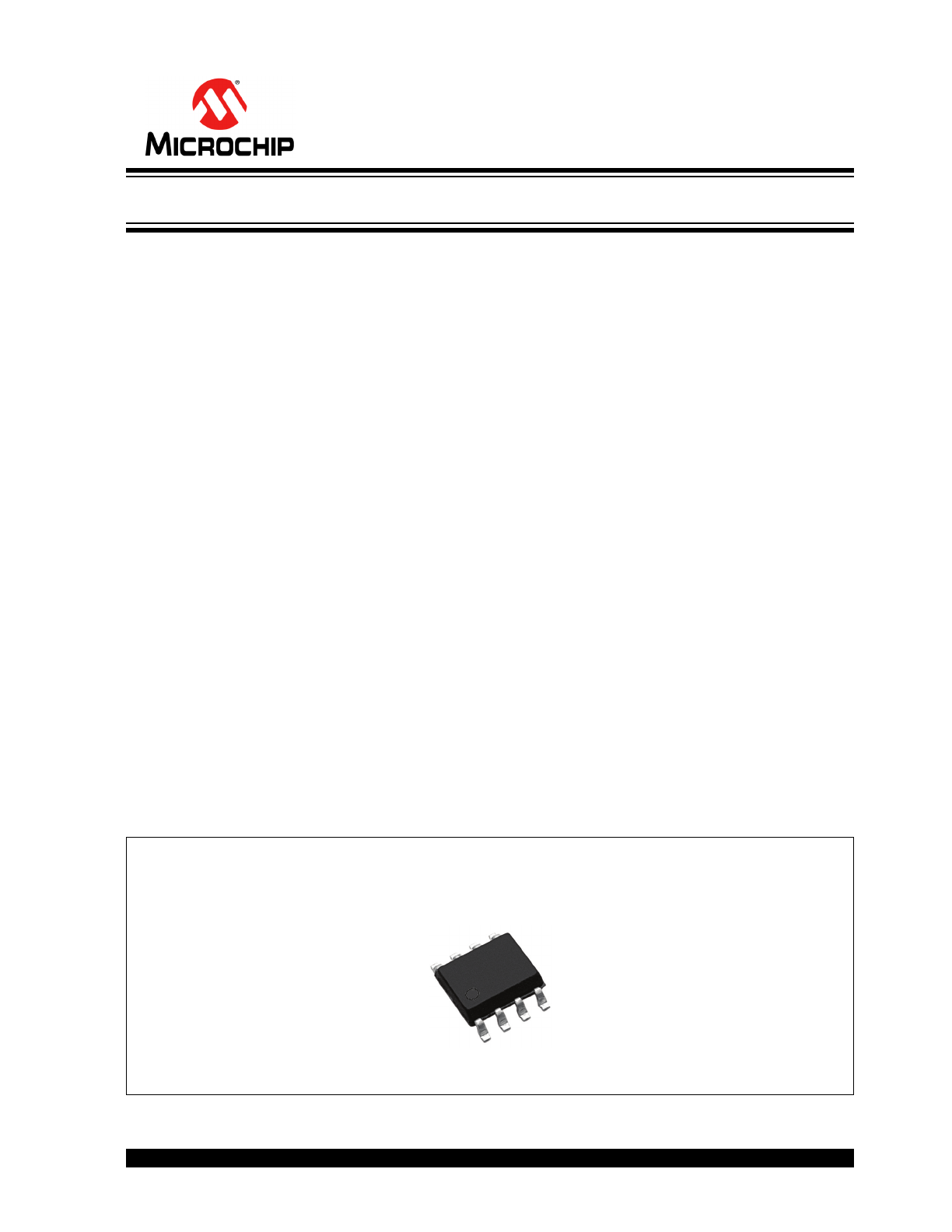
TC2320
Features
• Low Threshold
• Low On-resistance
• Low Input Capacitance
• Fast Switching Speeds
• Free from Secondary Breakdown
• Low Input and Output Leakage
• Independent, Electrically Isolated N-channel and
P-channel
Applications
• Medical Ultrasound Transmitters
• High-voltage Pulsers
• Amplifiers
• Buffers
• Piezoelectric Transducer Drivers
• General Purpose Line Drivers
• Logic-level Interface
General Description
The TC2320 consists of a high-voltage, low-threshold
N-channel and P-channel MOSFET in an 8-Lead SOIC
package. This Enhancement-mode (normally-off)
transistor uses an advanced vertical DMOS structure
and a well-proven silicon gate manufacturing process.
This combination produces a device with the power
handling capabilities of bipolar transistors and high
input impedance and positive temperature coefficient
inherent in MOS devices. Characteristic of all MOS
structures, this device is free from thermal runaway and
thermally induced secondary breakdown.
Microchip’s vertical DMOS FETs are ideally suited to a
wide range of switching and amplifying applications
where very low threshold voltage, high breakdown
voltage, high input impedance, low input capacitance
and fast switching speeds are desired.
Package Type
8-lead SOIC
See
Table 2-1
for pin information.
(Top view)
DP
DP
DN
DN
GP
SP
GN
SN
N-Channel and P-Channel Enhancement-Mode Dual MOSFET
TC2320
DS20005708A-page 2
2017 Microchip Technology Inc.
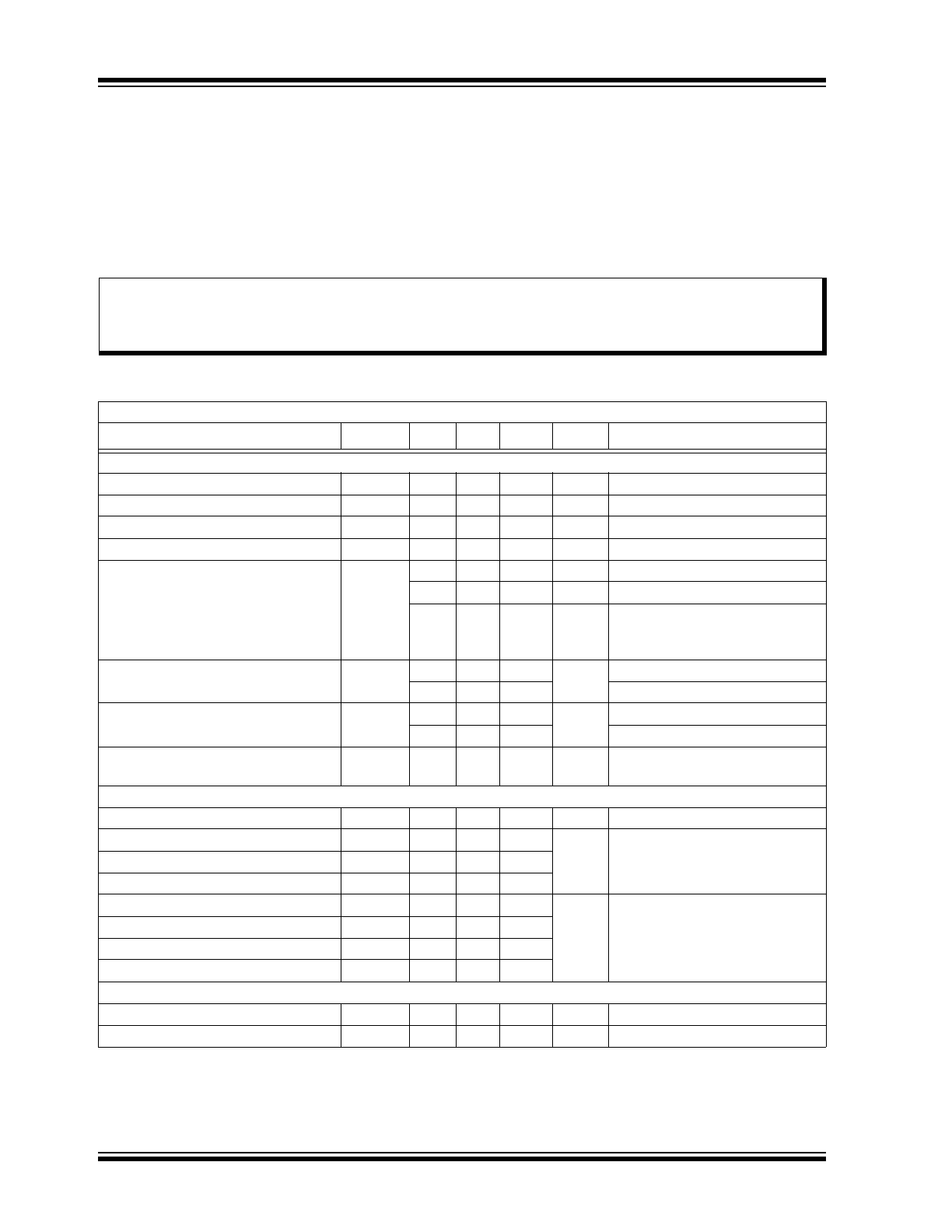
1.0
ELECTRICAL CHARACTERISTICS
Absolute Maximum Ratings†
Drain-to-source Voltage........................................................................................................................................ BV
DSS
Drain-to-gate Voltage ........................................................................................................................................... BV
DGS
Gate-to-source Voltage .......................................................................................................................................... ±20V
Operating Ambient Temperature, T
A
................................................................................................... –55°C to +150°C
Storage Temperature, T
S
..................................................................................................................... –55°C to +150°C
† Notice: Stresses above those listed under “Absolute Maximum Ratings” may cause permanent damage to the
device. This is a stress rating only, and functional operation of the device at those or any other conditions above those
indicated in the operational sections of this specification is not intended. Exposure to maximum rating conditions for
extended periods may affect device reliability.
N-CHANNEL DC AND AC ELECTRICAL CHARACTERISTICS
Electrical Specifications: Unless otherwise noted, T
A
= T
J
= +25°C.
Parameter
Sym.
Min.
Typ.
Max.
Unit
Conditions
DC PARAMETER (
Note 1
)
Drain-to-source Breakdown Voltage
BV
DSS
200
—
—
V
V
GS
= 0V, I
D
= 100 µA
Gate Threshold Voltage
V
GS(th)
0.6
—
2
V
V
GS
= V
DS
, I
D
= 1 mA
Change in V
GS(th)
with Temperature
∆V
GS(th)
—
—
–4.5
mV/°C V
GS
= V
DS
, I
D
= 1 mA (
Note 2
)
Gate Body Leakage Current
I
GSS
—
—
100
nA
V
GS
= ±20V, V
DS
= 0V
Zero-gate Voltage Drain Current
I
DSS
—
—
1
µA
V
GS
= 0V, V
DS
= 100V
—
—
10
µA
V
GS
= 0V, V
DS
= Maximum rating
—
—
1
mA
V
GS
= 0V, T
A
= 125°C,
V
DS
= 0.8 Maximum rating
(
Note 2
)
On-state Drain Current
I
D(ON)
0.6
—
—
A
V
GS
= 4.5V, V
DS
= 25V
1.2
—
—
V
GS
= 10V, V
DS
= 25V
Static Drain-to-Source On-state
Resistance
R
DS(ON)
—
—
8
Ω
V
GS
= 4.5V, I
D
= 150 mA
—
—
7
V
GS
= 10V, I
D
= 1A
Change in R
DS(ON)
with
Temperature
∆R
DS(ON)
—
—
1
%/°C
V
GS
= 4.5V, I
D
= 150 mA (
Note 2
)
AC PARAMETER (
Note 2
)
Forward Transconductance
G
FS
150
—
—
mmho V
DS
= 25V, I
D
= 200 mA
Input Capacitance
C
ISS
—
—
110
pF
V
GS
= 0V,
V
DS
= 25V,
f = 1 MHz
Common Source Output Capacitance
C
OSS
—
—
60
Reverse Transfer Capacitance
C
RSS
—
—
23
Turn-on Delay Time
t
d(ON)
—
—
20
ns
V
DD
= 25V,
I
D
= 150 mA,
R
GEN
= 25Ω
Rise Time
t
r
—
—
15
Turn-off Delay Time
t
d(OFF)
—
—
25
Fall Time
t
f
—
—
25
DIODE PARAMETER
Diode Forward Voltage Drop
V
SD
—
—
1.8
V
V
GS
= 0V, I
SD
= 200 mA (
Note 1
)
Reverse Recovery Time
t
rr
—
300
—
ns
V
GS
= 0V, I
SD
= 200 mA (
Note 2
)
Note 1: Unless otherwise stated, all DC parameters are 100% tested at +25°C.
Pulse test: 300 µs pulse, 2% duty cycle.
2: Specification is obtained by characterization and is not 100% tested.
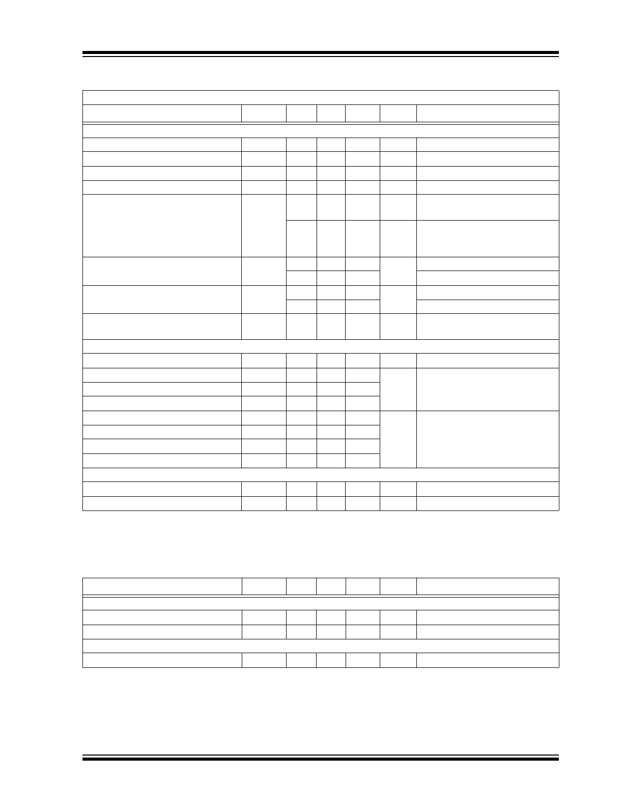
P-CHANNEL DC AND AC ELECTRICAL CHARACTERISTICS
Electrical Specifications: Unless otherwise noted, T
A
= T
J
= +25°C.
Parameter
Sym.
Min.
Typ.
Max.
Unit
Conditions
DC PARAMETER (
Note 1
)
Drain-to-source Breakdown Voltage
BV
DSS
–200
—
—
V
V
GS
= 0V, I
D
= –2 mA
Gate Threshold Voltage
V
GS(th)
–1
—
–2.4
V
V
GS
= V
DS
, I
D
= –1 mA
Change in V
GS(th)
with Temperature
∆V
GS(th)
—
—
4.5
mV/°C V
GS
= V
DS
, I
D
= –1 mA (
Note 2
)
Gate Body Leakage
I
GSS
—
—
–100
nA
V
GS
= ±20V, V
DS
= 0V
Zero-gate Voltage Drain Current
I
DSS
—
—
–10
µA
V
GS
= 0V,
V
DS
= Maximum rating
—
—
–1
mA
V
GS
= 0V, T
A
= 125°C,
V
DS
= 0.8 Maximum rating
(
Note 2
)
On-state Drain Current
I
D(ON)
–0.25 –0.7
—
A
V
GS
= –4.5V, V
DS
= –25V
–0.75 –2.1
—
V
GS
= –10V, V
DS
= –5V
Static Drain-to-Source On-state
Resistance
R
DS(ON)
—
10
15
Ω
V
GS
= –4.5V, I
D
= –100 mA
—
8
12
V
GS
= –10V, I
D
= –200 mA
Change in R
DS(ON)
with
Temperature
∆
RDS(ON)
—
—
1.7
%/°C
V
GS
= –10V, I
D
= –200 mA
(
Note 2
)
AC PARAMETER (
Note 2
)
Forward Transconductance
G
FS
100
250
—
mmho V
DS
= –25V, I
D
= –200 mA
Input Capacitance
C
ISS
—
75
125
pF
V
GS
= 0V,
V
DS
= –25V,
f = 1 MHz
Common Source Output Capacitance
C
OSS
—
20
85
Reverse Transfer Capacitance
C
RSS
—
10
35
Turn-on Delay Time
t
d(ON)
—
—
10
ns
V
DD
= –25V,
I
D
= –0.75A,
R
GEN
= 25Ω
Rise Time
t
r
—
—
15
Turn-on Delay Time
t
d(OFF)
—
—
20
Fall Time
t
f
—
—
15
DIODE PARAMETER
Diode Forward Voltage Drop
V
SD
—
—
–1.8
V
V
GS
= 0V, I
SD
= –0.5A (
Note 1
)
Reverse Recovery Time
t
rr
—
300
—
ns
V
GS
= 0V, I
SD
= –0.5A (
Note 2
)
Note 1: Unless otherwise stated, all DC parameters are 100% tested at +25°C. Pulse test: 300 µs pulse, 2% duty
cycle.
2: Specification is obtained by characterization and is not 100% tested.
TEMPERATURE SPECIFICATIONS
Parameter
Sym.
Min.
Typ.
Max.
Unit
Conditions
TEMPERATURE RANGE
Operating Ambient Temperature
T
A
–55
—
+150
°C
Storage Temperature
T
S
–55
—
+150
°C
PACKAGE THERMAL RESISTANCE
8-lead SOIC
JA
—
101
—
°C/W
Note 1
2017 Microchip Technology Inc.
DS20005708A-page 3
TC2320
Note 1: 1 oz., four-layer, 3” x 4” PCB

TC2320
DS20005708A-page 4
2017 Microchip Technology Inc.
2.0
PIN DESCRIPTION
Table 2-1
shows the description of pins in TC2320.
Refer to
Package Type
for the location of pins.
TABLE 2-1:
PIN FUNCTION TABLE
Pin Number
Pin Name
Description
1
SN
Source N-channel
2
GN
Gate N-channel
3
SP
Source P-channel
4
GP
Gate P-channel
5
DP
Drain P-channel
6
DP
Drain P-channel
7
DN
Drain N-channel
8
DN
Drain N-channel
2017 Microchip Technology Inc.
DS20005708A-page 5
TC2320
3.0
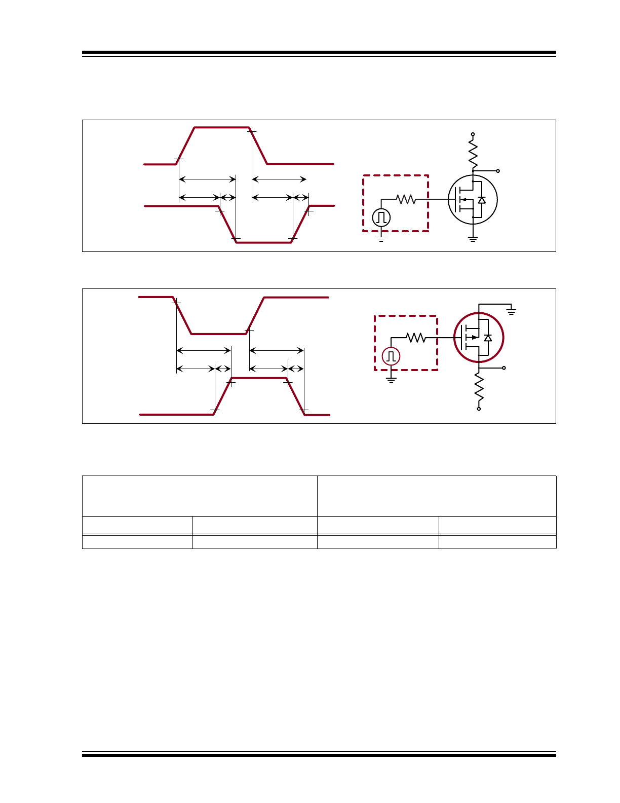
FUNCTIONAL DESCRIPTION
Figure 3-1
and
Figure 3-2
illustrate the switching
waveforms and test circuits for TC2320.
VDD
R
L
OUTPUT
D.U.T.
10V
INPUT
0V
VDD
OUTPUT
0V
10%
90%
90%
10%
90%
10%
R
GEN
Input
Pulse
Generator
t
r
t
f
t
d(ON)
t
(ON)
t
d(OFF)
t
(OFF)
FIGURE 3-1:
N-channel Switching Waveforms and Test Circuit.
VDD
R
L
OUTPUT
D.U.T.
R
GEN
Input
Pulse
Generator
0V
INPUT
-10V
0V
OUTPUT
VDD
t
r
t
f
t
d(ON)
t
(ON)
90%
10%
90%
10%
10%
90%
t
d(OFF)
t
(OFF)
FIGURE 3-2:
P-channel Switching Waveforms and Test Circuit.
TABLE 3-1:
PRODUCT SUMMARY
BV
DSS
/BV
DGS
(V)
R
DS(ON)
(Maximum)
(Ω)
N-Channel
P-Channel
N-Channel
P-Channel
200
–200
7
12
TC2320
DS20005708A-page 6
2017 Microchip Technology Inc.
4.0
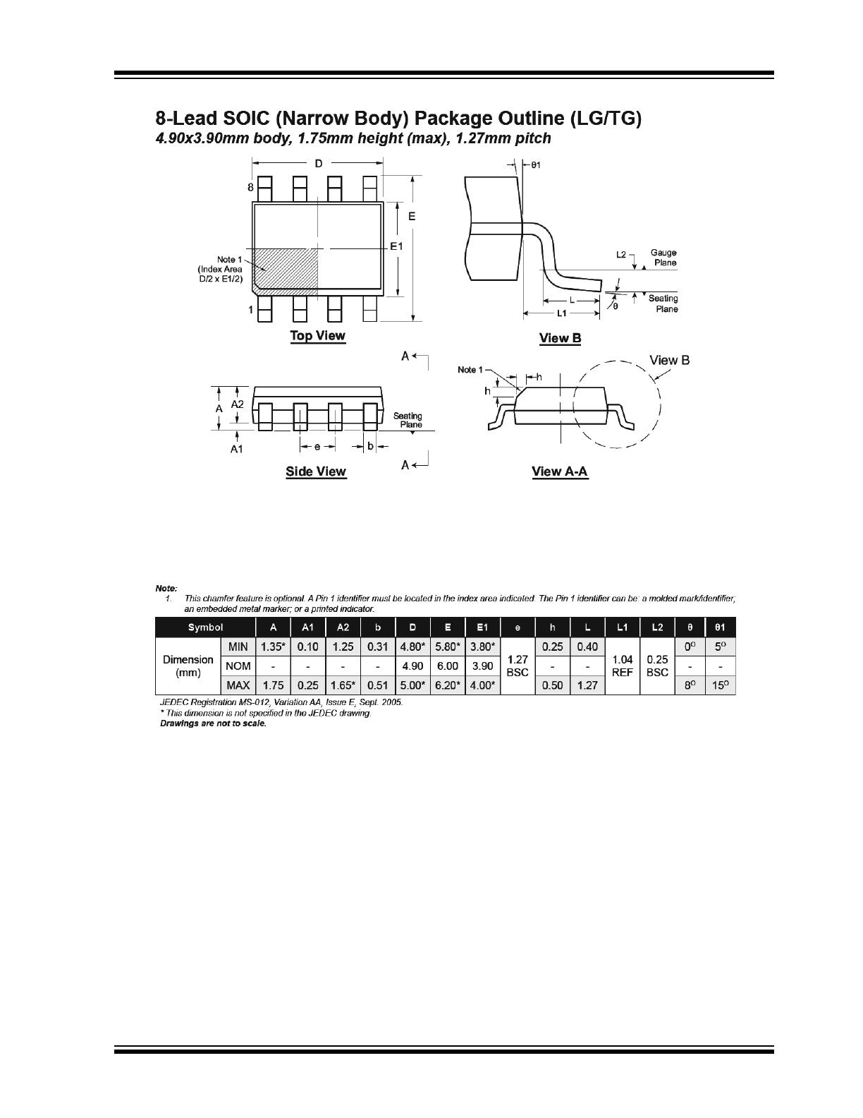
PACKAGING INFORMATION
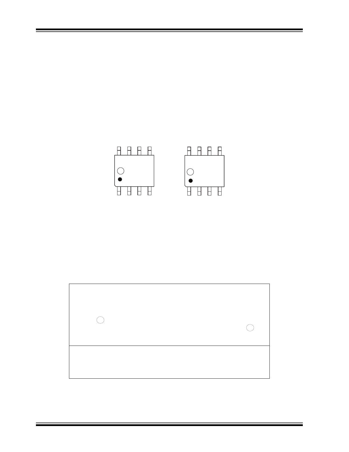
4.1
Package Marking Information
Legend: XX...X
Product Code or Customer-specific information
Y
Year code (last digit of calendar year)
YY
Year code (last 2 digits of calendar year)
WW
Week code (week of January 1 is week ‘01’)
NNN
Alphanumeric traceability code
Pb-free JEDEC
®
designator for Matte Tin (Sn)
*
This package is Pb-free. The Pb-free JEDEC designator ( )
can be found on the outer packaging for this package.
Note:
In the event the full Microchip part number cannot be marked on one line, it will
be carried over to the next line, thus limiting the number of available
characters for product code or customer-specific information. Package may or
not include the corporate logo.
3
e
3
e
8-lead SOIC
Example
NNN
XXXXXXXX
YYWW
e3
896
TC2320TG
1737
e3
Note: For the most current package drawings, see the Microchip Packaging Specification at www.microchip.com/packaging.
2017 Microchip Technology Inc.
DS20005708A-page 7
TC2320

TC2320
DS20005708A-page 8
2017 Microchip Technology Inc.
NOTES:

2017 Microchip Technology Inc.
DS20005708A-page 9
TC2320
APPENDIX A: REVISION HISTORY
Revision A (June 2017)
• Converted Supertex Doc# DSFP-TC2320 to
Microchip DS20005708A
• Changed packaging format
• Changed the packaging quantity of the 8-lead
SOIC TG package from 2000/Reel to 3300/Reel
• Made minor text changes throughout the
document

TC2320
DS20005708A-page 10
2017 Microchip Technology Inc.
PRODUCT IDENTIFICATION SYSTEM
To order or obtain information, e.g., on pricing or delivery, contact your local Microchip representative or sales office
.
Example:
a) TC2320TG-G
:
N-Channel and P-Channel
Enhancement-Mode Dual MOSFET,
8-lead SOIC, 3300/Reel
PART NO.
Device
Device:
TC2320
=
N-Channel and P-Channel
Enhancement-Mode Dual MOSFET
Package:
TG
=
8-lead SOIC
Environmental:
G
=
Lead (Pb)-free/RoHS-compliant Package
Media Type:
(blank)
=
3300/Reel for a TG Package
XX
Package
-
X - X
Environmental Media Type
Options