
2001-2015 Microchip Technology Inc.
DS20001392E-page 1
TC1413/TC1413N
Features
• Latch-Up Protected: Withstands 500 mA Reverse
Current
• Input Withstands Negative Inputs Up to 5V
• Electrostatic Discharge (ESD) Protected: 2.0 kV
(HBM) and 400V (MM)
• High Peak Output Current: 3A
• Wide Input Supply Voltage Operating Range:
- 4.5V to 16V
• High Capacitive Load Drive Capability:
- 1800 pF in 20 ns
• Short Delay Time: 35 ns typical
• Matched Delay Times
• Low Supply Current
- With Logic ‘1’ Input: 500 µA
- With Logic ‘0’ Input: 100 µA
• Low Output Impedance: 2.7
• Available in Space-Saving 8-pin MSOP Package
• Pinout - same as TC1410/TC1411/TC1412
Applications
• Switch Mode Power Supplies
• Line Drivers
• Pulse Transformer Drive
• Relay Driver
General Description
The TC1413/TC1413N are 3A CMOS buffers/drivers.
They do not latch up under any conditions within their
power and voltage ratings. They are not subject to
damage when up to 5V of noise spiking of either
polarity occurs on the ground pin. They can accept,
without damage or logic upset, up to 500 mA of current
of either polarity being forced back into their output. All
terminals are fully protected against electrostatic
discharge (ESD) up to 2.0 kV (HBM) and 400V (MM).
As MOSFET drivers, the TC1413/TC1413N can easily
charge a 1800 pF gate capacitance in 20 ns with
matched rise and fall times. To ensure the MOSFET’s
intended state will not be affected even by large
transients, low enough impedance in both the ‘On’ and
‘Off’ states are provided. The leading and trailing edge
propagation delay times are also matched to allow
driving short-duration inputs with greater accuracy.
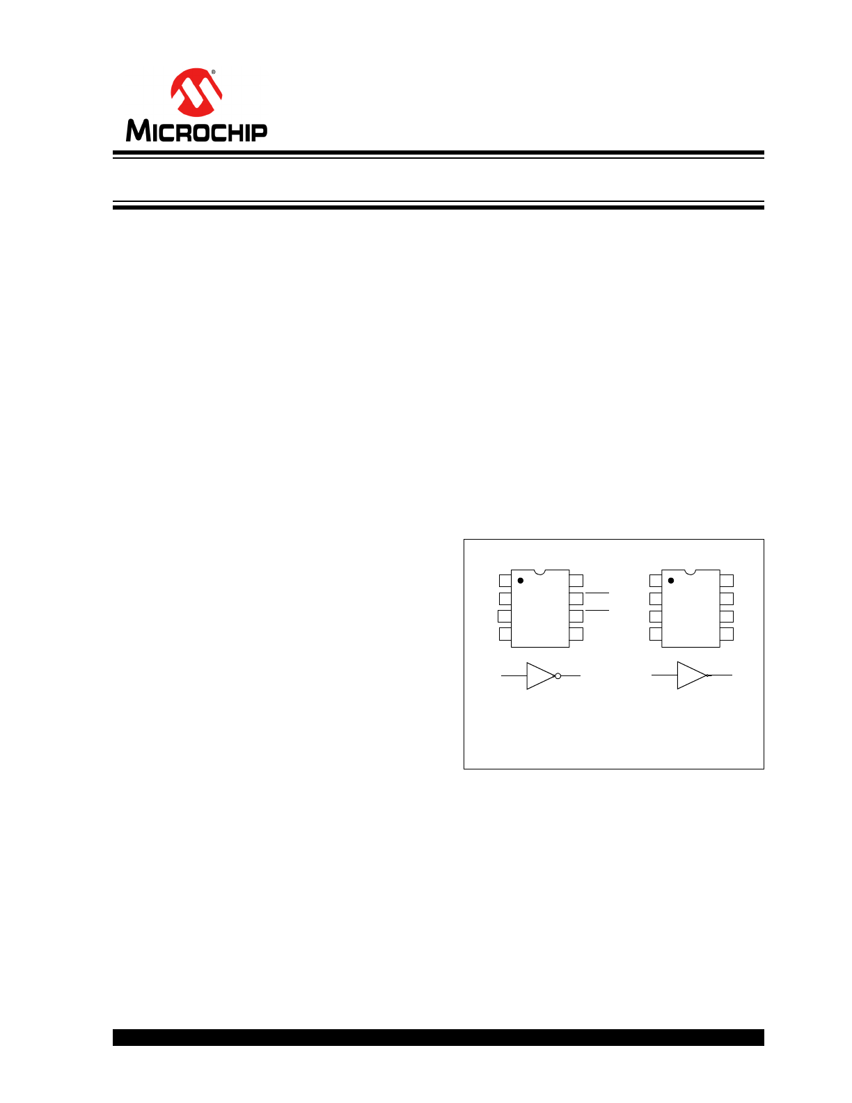
Package Type
2
6,7
Inverting
8-Pin MSOP/PDIP/SOIC
1
2
3
4
V
DD
5
6
7
8
OUT
GND
V
DD
IN
NC
GND
OUT
TC1413
NC = No Internal Connection
2
6,7
Non-Inverting
1
2
3
4
5
6
7
8
TC1413N
V
DD
IN
NC
GND
V
DD
OUT
GND
OUT
Note:
For proper operation, duplicate pins
must be connected together.
3A High-Speed MOSFET Drivers
TC1413/TC1413N
DS20001392E-page 2
2001-2015 Microchip Technology Inc.
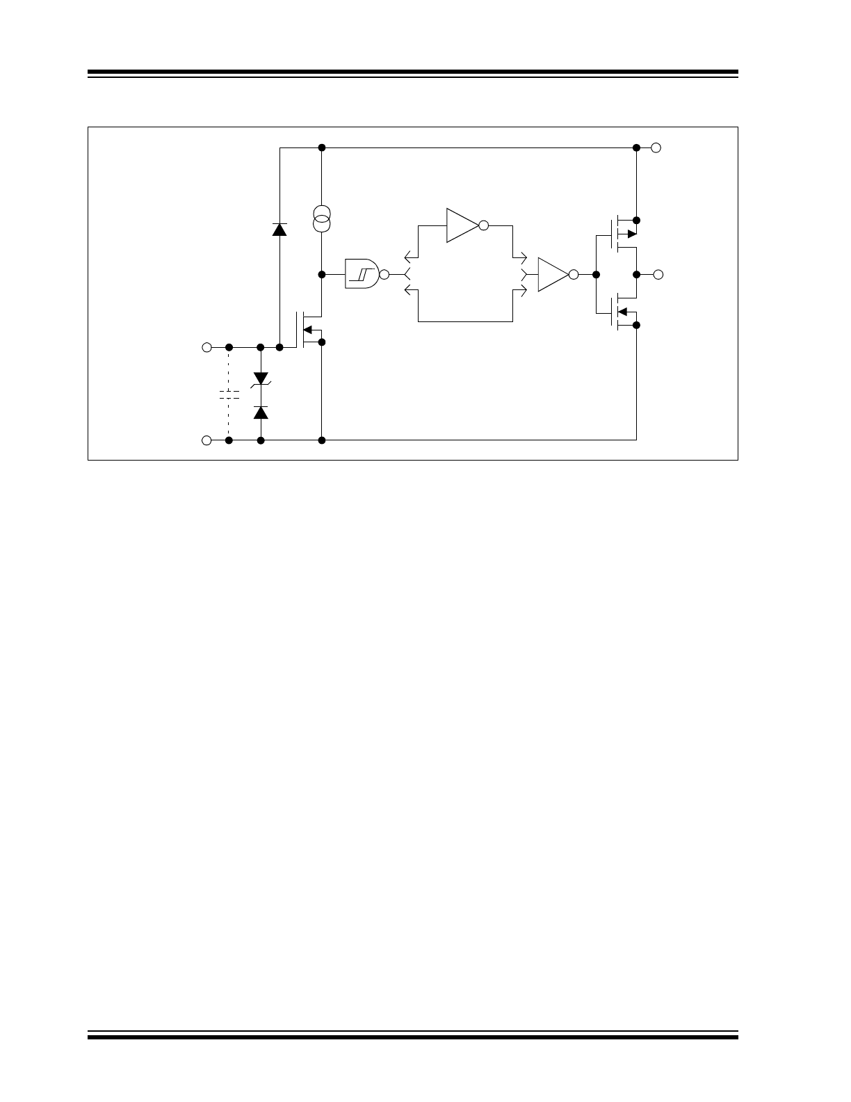
Functional Block Diagram
Effective
Input C = 10 pF
Output
Input
GND
V
DD
300 mV
4.7V
Inverting
Non-Inverting
Outputs
Outputs
TC1413
TC1413N
2001-2015 Microchip Technology Inc.
DS20001392E-page 3
TC1413/TC1413N
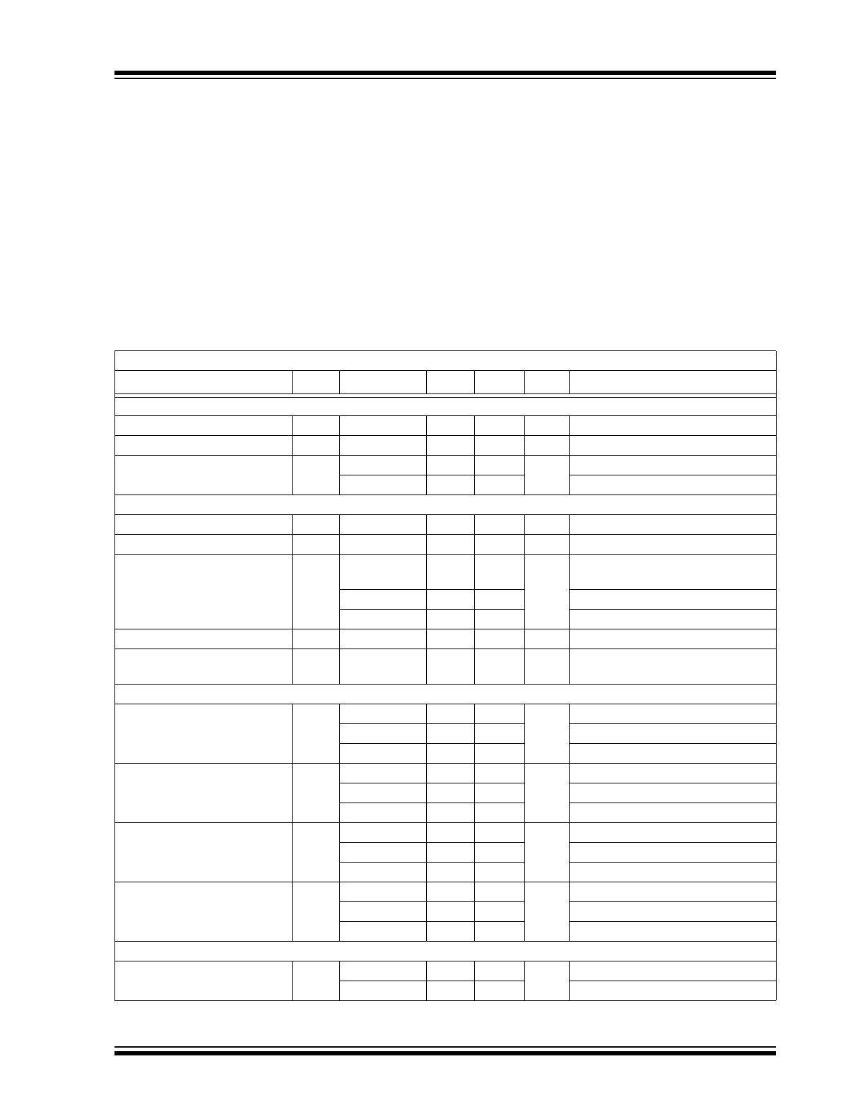
1.0
ELECTRICAL
CHARACTERISTICS
Absolute Maximum Ratings†
Supply Voltage .....................................................+20V
Input Voltage ...................... V
DD
+ 0.3V to GND – 5.0V
Power Dissipation (T
A
70°C)
MSOP .......................................................... 340 mW
PDIP ............................................................ 730 mW
SOIC............................................................ 470 mW
Storage Temperature Range.............. -65°C to +150°C
Maximum Junction Temperature...................... +150ºC
† Notice: Stresses above those listed under "Absolute
Maximum Ratings" may cause permanent damage to
the device. These are stress ratings only and functional
operation of the device at these or any other conditions
above those indicated in the operation sections of the
specifications is not implied. Exposure to Absolute
Maximum Rating conditions for extended periods may
affect device reliability.
DC ELECTRICAL CHARACTERISTICS
Electrical Specifications: Unless otherwise noted, T
A
= +25°C, with 4.5V
V
DD
16V.
Parameters
Sym.
Min.
Typ.
Max.
Units
Conditions
Input
Logic ‘1’, High Input Voltage
V
IH
2.0
—
—
V
Logic ‘0’, Low Input Voltage
V
IL
—
—
0.8
V
Input Current
I
IN
-1.0
—
1.0
µA
0V
V
IN
V
DD,
T
A
= +25°C
-10
—
10
-40°C
T
A
+85°C
Output
High Output Voltage
V
OH
V
DD
– 0.025
—
—
V
DC Test
Low Output Voltage
V
OL
—
—
0.025
V
DC Test
Output Resistance
R
O
—
2.7
4.0
V
DD
= 16V, I
O
= 10 mA,
T
A
= +25°C
—
3.3
5.0
0°C
T
A
+70°C
—
3.3
5.0
-40°C
T
A
+85°C
Peak Output Current
I
PK
—
3.0
—
A
V
DD
= 16V
Latch-Up Protection
Withstand Reverse Current
I
REV
—
0.5
—
A
Duty cycle
2%, t 300 µs,
V
DD
= 16V
Switching Time (
Note 1
)
Rise Time
t
R
—
20
28
ns
T
A
= +25°C
—
22
33
0°C
T
A
+70°C
—
24
33
-40°C
T
A
+85°C,
Figure 4-1
Fall Time
t
F
—
20
28
ns
T
A
= +25°C
—
22
33
0°C
T
A
+70°C
—
24
33
-40°C
T
A
+85°C,
Figure 4-1
Delay Time
t
D1
—
35
45
ns
T
A
= +25°C,
—
40
50
0°C
T
A
+70°C
—
40
50
-40°C
T
A
+85°C,
Figure 4-1
Delay Time
t
D2
—
35
45
ns
T
A
= +25°C
—
40
50
0°C
T
A
+70°C
—
40
50
-40°C
T
A
+85°C,
Figure 4-1
Power Supply
Power Supply Current
I
S
—
0.5
1.0
mA
V
IN
= 3V, V
DD
= 16V
—
0.1
0.15
V
IN
= 0V
Note 1:
Switching times ensured by design.
TC1413/TC1413N
DS20001392E-page 4
2001-2015 Microchip Technology Inc.
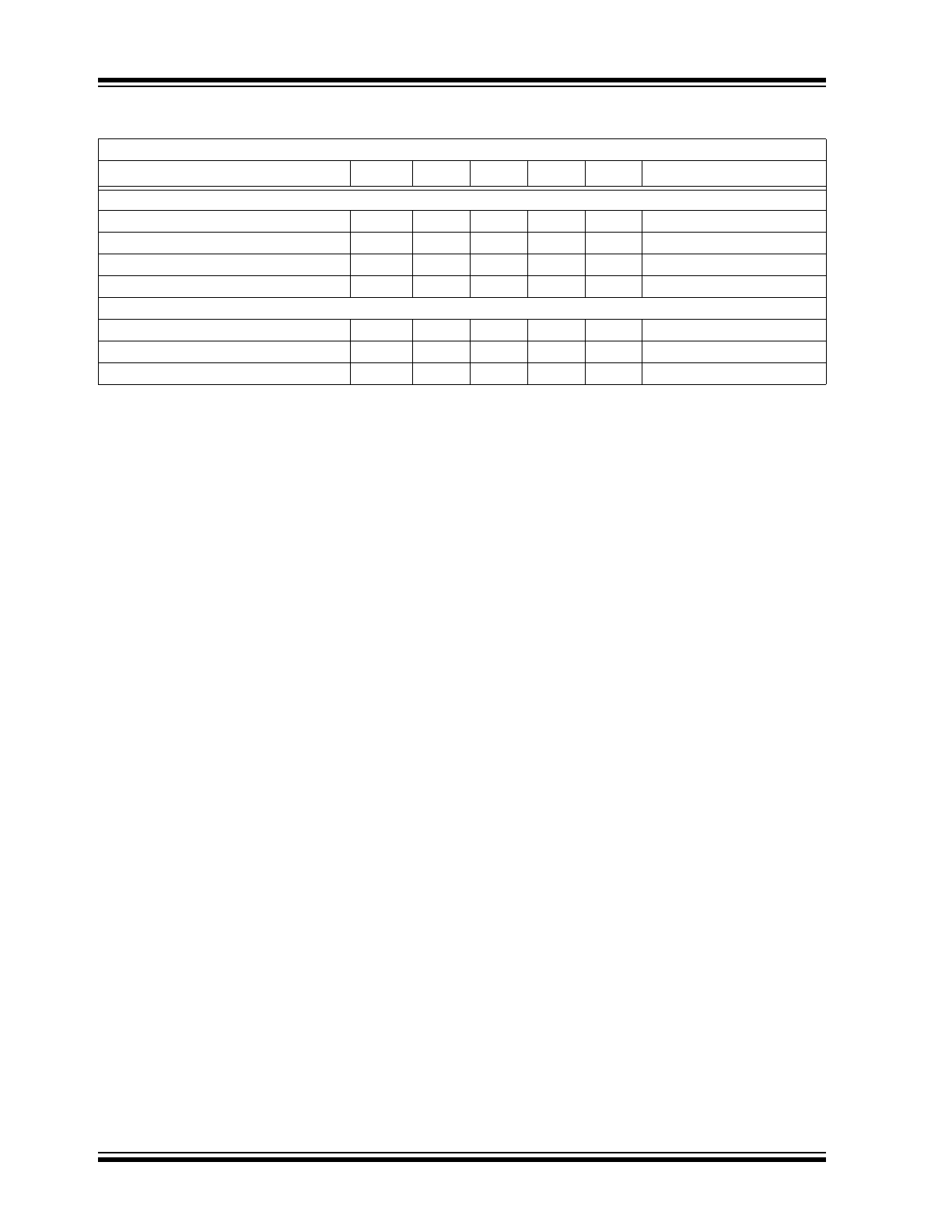
TEMPERATURE CHARACTERISTICS
Electrical Specifications: Unless otherwise noted, all parameters apply with 4.5V
V
DD
18V.
Parameters
Sym.
Min.
Typ.
Max.
Units
Conditions
Temperature Ranges
Specified Temperature Range (C)
T
A
0
—
+70
ºC
Specified Temperature Range (E)
T
A
-40
—
+85
ºC
Maximum Junction Temperature
T
J
—
—
+150
ºC
Storage Temperature Range
T
A
-65
—
+150
ºC
Package Thermal Resistances
Thermal Resistance, 8L-MSOP
JA
—
211
—
ºC/W
Thermal Resistance, 8L-PDIP
JA
—
89.3
—
ºC/W
Thermal Resistance, 8L-SOIC
JA
—
149.5
—
ºC/W
2001-2015 Microchip Technology Inc.
DS20001392E-page 5
TC1413/TC1413N
2.0
TYPICAL PERFORMANCE CURVES
Note: Unless otherwise indicated, over operating temperature range with 4.5V
V
DD
16V.
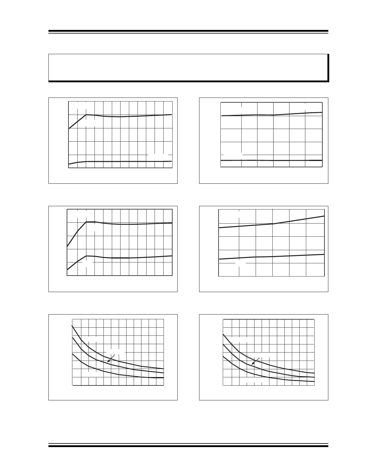
FIGURE 2-1:
Quiescent Supply Current
vs. Supply Voltage.
FIGURE 2-2:
Input Threshold vs. Supply
Voltage.
FIGURE 2-3:
High State Output
Resistance vs. Supply Voltage.
FIGURE 2-4:
Quiescent Supply Current
vs. Temperature.
FIGURE 2-5:
Input Threshold vs.
Temperature.
FIGURE 2-6:
Low State Output
Resistance vs. Supply Voltage.
Note:
The graphs and tables provided following this note are a statistical summary based on a limited number of
samples and are provided for informational purposes only. The performance characteristics listed herein
are not tested or guaranteed. In some graphs or tables, the data presented may be outside the specified
operating range (e.g., outside specified power supply range) and therefore outside the warranted range.
0
100
200
300
400
500
16
14
12
10
8
6
4
V
IN
= 3V
V
IN
= 0V
T
A
= +25
°C
I
SUPPLY
(
µ
A)
V
DD
(V)
V
DD
(V)
V
THRESHOLD
(V)
1.1
1.2
1.3
1.4
1.5
1.6
16
14
12
10
8
6
4
V
IH
V
IL
T
A
= +25
°C
R
DS-ON
(Ohms)
V
DD
(V)
1
2
3
4
5
6
7
8
9
16
14
12
10
8
6
4
T
A
= -40
°C
T
A
= +25
°C
T
A
= +85
°C
I
SUPPLY
(
µ
A)
TEMPERATURE (
°C)
-40
-20
0
20
40
60
80
0
100
200
300
400
500
V
IN
= 3V
V
IN
= 0V
V
SUPPLY
= 16V
-40
-20
0
20
40
60
80
1.1
1.2
1.3
1.4
1.5
1.6
V
SUPPLY
= 16V
TEMPERATURE (
°C)
V
THRESHOLD
(V)
V
IH
V
IL
R
DS-ON
(Ohms)
V
DD
(V)
1
2
3
4
5
6
7
8
9
16
14
12
10
8
6
4
T
A
= -40
°C
T
A
= +25
°C
T
A
= +85
°C
TC1413/TC1413N
DS20001392E-page 6
2001-2015 Microchip Technology Inc.
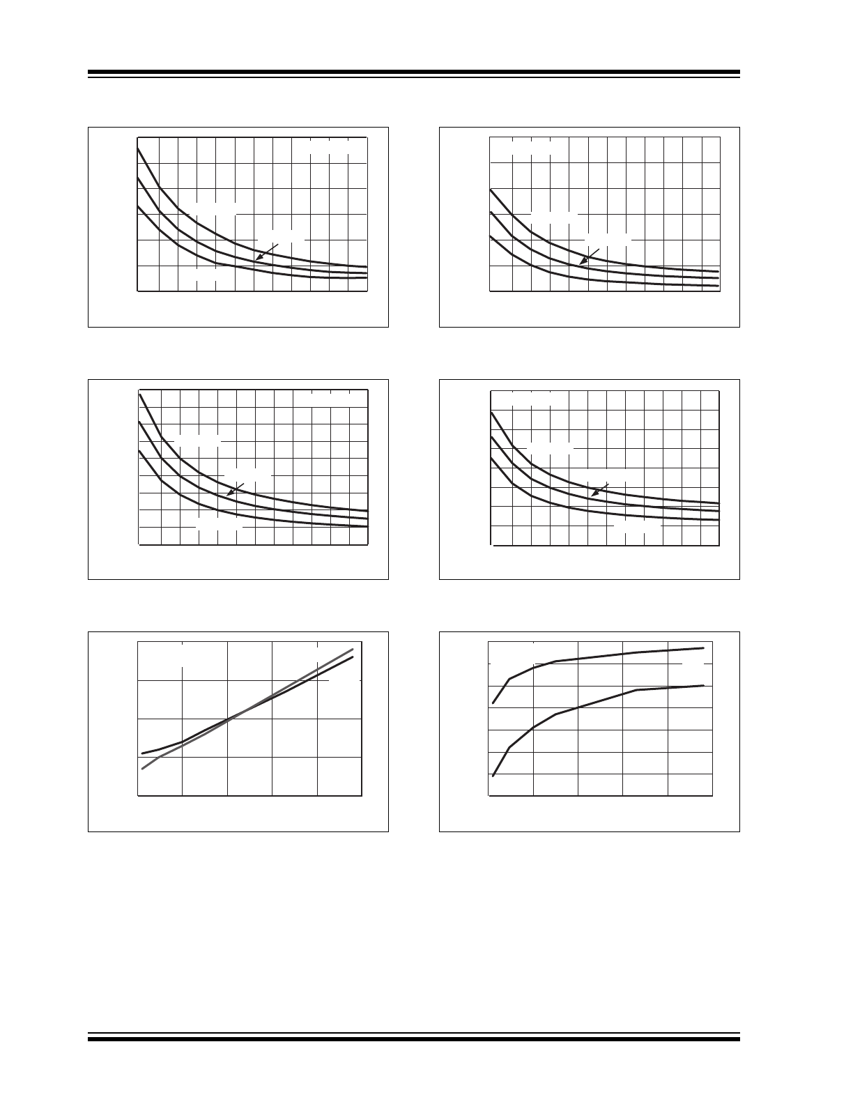
Note: Unless otherwise indicated, over operating temperature range with 4.5V
V
DD
16V.
FIGURE 2-7:
Rise Time vs. Supply
Voltage.
FIGURE 2-8:
Propagation Delay vs.
Supply Voltage.
FIGURE 2-9:
Rise and Fall Times vs.
Capacitive Load.
FIGURE 2-10:
Fall Time vs. Supply
Voltage.
FIGURE 2-11:
Propagation Delay vs.
Supply Voltage.
FIGURE 2-12:
Propagation Delays vs.
Capacitive Load.
V
DD
(V)
t
RISE
(nsec)
10
20
30
40
50
60
70
16
14
12
10
8
6
4
T
A
= +25
°C
T
A
= +85
°C
C
LOAD
= 1800 pF
T
A
= -40
°C
V
DD
(V)
t
D1
(nsec)
20
30
40
50
60
70
80
90
100
110
16
14
12
10
8
6
4
T
A
= -40
°C
T
A
= +25
°C
T
A
= +85
°C
C
LOAD
= 1800 pF
t
RISE
, t
FALL
(nsec)
C
LOAD
(pF)
0
1000
2000
3000
4000
5000
0
10
20
30
40
t
FALL
t
RISE
T
A
= +25
°C
V
DD
= 16V
t
FALL
(nsec)
10
20
30
40
50
60
70
16
14
12
10
8
6
4
V
DD
(V)
T
A
= +25
°C
T
A
= +85
°C
C
LOAD
= 1800 pF
T
A
= -40
°C
V
DD
(V)
t
D2
(nsec)
20
30
40
50
60
70
80
90
100
16
14
12
10
8
6
4
C
LOAD
= 1800 pF
T
A
= -40
°C
T
A
= +25
°C
T
A
= +85
°C
C
LOAD
(pF)
Propagation Delays (nsec)
0
1000
2000
3000
4000
5000
28
29
30
31
32
33
34
35
t
D2
t
D1
T
A
= +25
°C
V
DD
= 16V
2001-2015 Microchip Technology Inc.
DS20001392E-page 7
TC1413/TC1413N
3.0
PIN DESCRIPTIONS
The descriptions of the pins are listed in
Table 3-1
.
.
3.1
Supply Input (V
DD
)
The V
DD
input is the bias supply for the MOSFET driver
and is rated for 4.5V to 16V with respect to the ground
pin. The V
DD
input should be bypassed to ground with
a local ceramic capacitor. The value of the capacitor is
chosen based on the capacitive load that is being
driven. A value of 1.0 µF is suggested.
3.2
Control Input (IN)
The MOSFET driver input is a high-impedance,
TTL/CMOS-compatible input. The input has 300 mV of
hysteresis between the high and low thresholds which
prevents output glitching even when the rise and fall
time of the input signal is very slow.
3.3
CMOS Push-Pull Output
(OUT, OUT)
The MOSFET driver output is a low-impedance, CMOS
push-pull style output, capable of driving a capacitive
load with 3A peak currents.
3.4
Ground (GND)
The ground pins are the return path for the bias current
and for the high peak currents that discharge the load
capacitor. The ground pins should be tied into a ground
plane or have very short traces to the bias supply
source return.
3.5
No Connect (NC)
No internal connection.
TABLE 3-1:
PIN FUNCTION TABLE
Pin
No.
TC1413
MSOP, PDIP, SOIC
TC1413N
MSOP, PDIP, SOIC
Description
1
V
DD
V
DD
Supply input, 4.5V to 16V
2
IN
IN
Control input
3
NC
NC
No connection
4
GND
GND
Ground
5
GND
GND
Ground
6
OUT
OUT
CMOS push-pull output, common to pin 7
7
OUT
OUT
CMOS push-pull output, common to pin 6
8
V
DD
V
DD
Supply input, 4.5V to 16V
TC1413/TC1413N
DS20001392E-page 8
2001-2015 Microchip Technology Inc.
4.0
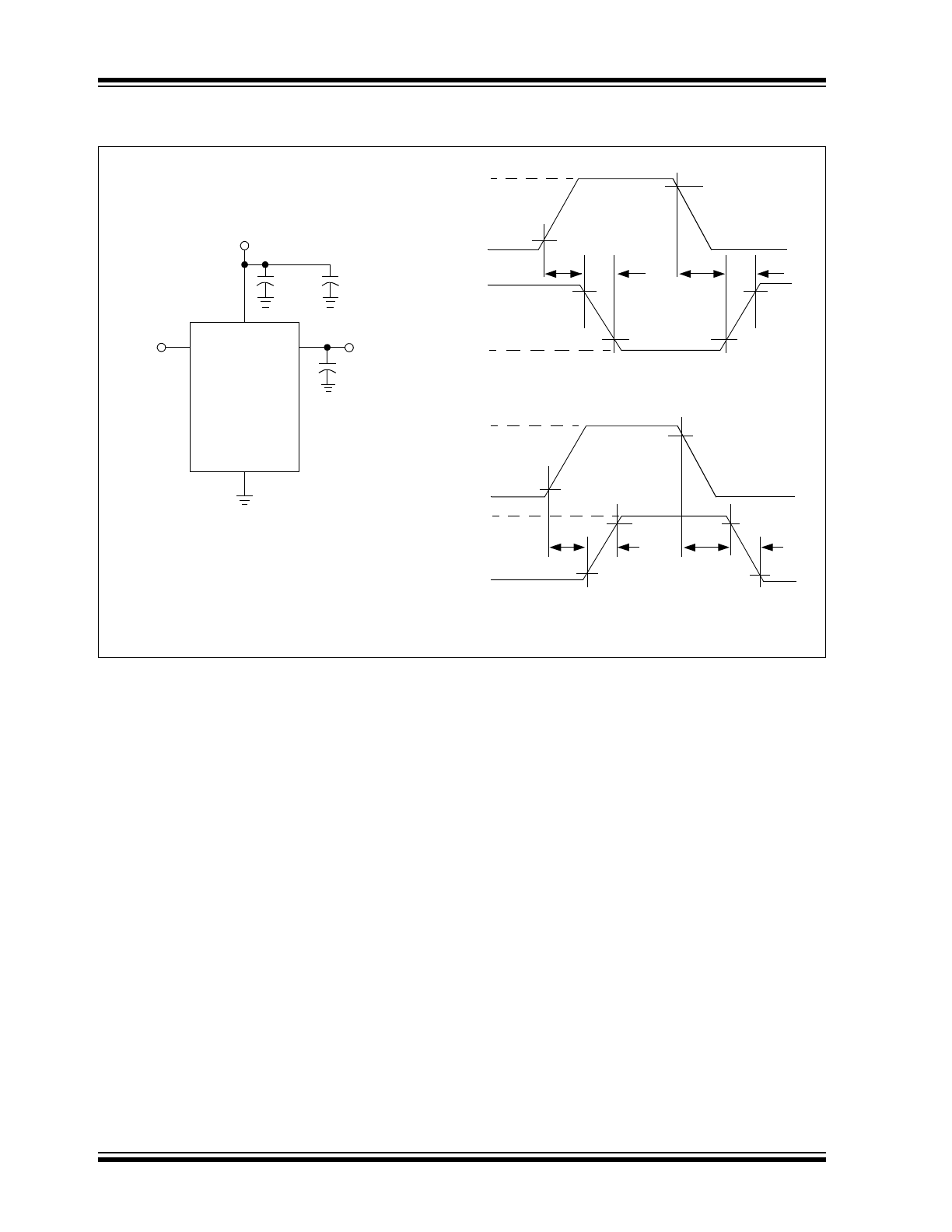
APPLICATION INFORMATION
FIGURE 4-1:
Switching Time Test Circuit.
C
L
= 1800 pF
0.1 µF
1.0 µF
Inverting Driver
Non-Inverting Driver
Input
V
DD
= 16V
Input
Output
t
D1
t
F
t
R
t
D2
Input: 100 kHz,
square wave,
t
RISE
= t
FALL
10 ns
Output
Input
Output
t
D1
t
F
t
R
t
D2
+5V
10%
90%
10%
90%
10%
90%
V
DD
0V
90%
10%
10%
10%
90%
+5V
V
DD
0V
0V
0V
90%
4, 5
2
6, 7
1, 8
TC1413
TC1413N
TC1413
TC1413N
2001-2015 Microchip Technology Inc.
DS20001392E-page 9
TC1413/TC1413N
5.0
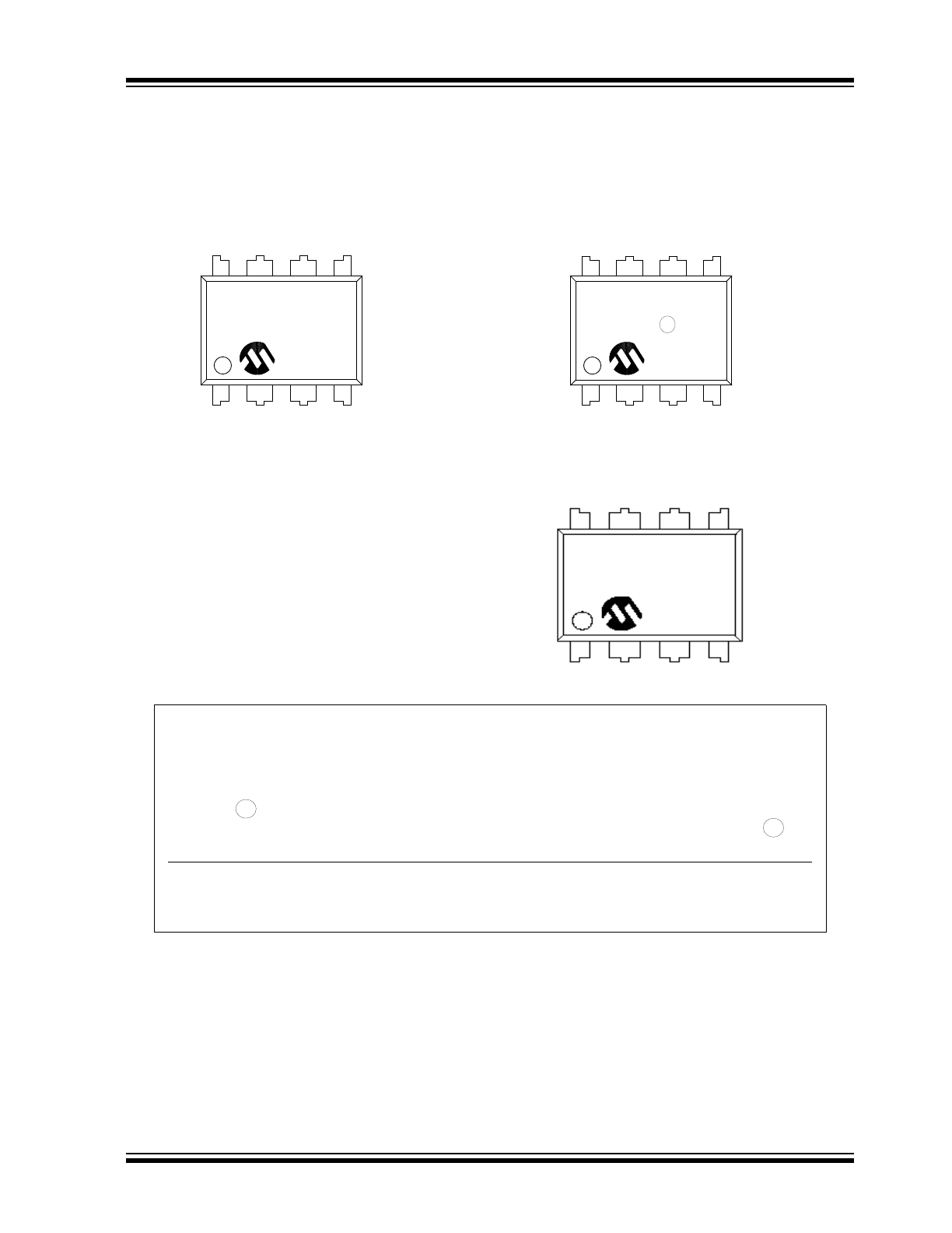
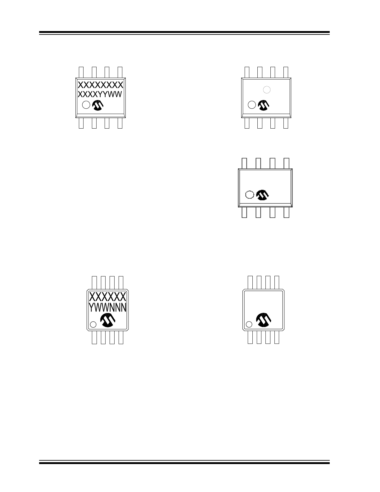
PACKAGING INFORMATION
5.1
Package Marking Information
XXXXXXXX
XXXXXNNN
YYWW
8-Lead PDIP (300 mil)
Example
TC1413
CPA^^ 256
1318
3
e
OR
TC1413
CPA256
1318
Legend: XX...X
Customer-specific information
Y
Year code (last digit of calendar year)
YY
Year code (last 2 digits of calendar year)
WW
Week code (week of January 1 is week ‘01’)
NNN
Alphanumeric traceability code
RoHS Compliant JEDEC
®
designator for Matte Tin (Sn)
*
This package is RoHS Compliant. The RoHS Compliant JEDEC designator ( )
can be found on the outer packaging for this package.
Note:
In the event the full Microchip part number cannot be marked on one line, it will be carried over
to the next line, thus limiting the number of available characters for customer-specific
information.
3
e
3
e
TC1413/TC1413N
DS20001392E-page 10
2001-2015 Microchip Technology Inc.
8-Lead SOIC (3.90 mm)
Example
NNN
TC1413C
OA^^ 1318
256
3
e
OR
8-Lead MSOP (3x3 mm)
Example
1413E
318256
TC1413
COA1318
256