
2007-2011 Microchip Technology Inc.
DS22035D-page 1
TC1270A/70AN/71A
Features:
• Precision Voltage Monitor
- 2.63V, 2.93V, 3.08V, 4.38V and 4.63V Trip
Points (Typical)
• Manual Reset Input
• Reset Time-Out Delay:
- Standard: 280 ms (Typical)
- Optional: 2.19 ms, and 35 ms (Typical)
• Power Consumption
15 µA max
• No glitches on outputs during power-up
• Active Low Output Options:
- Push-Pull Output and Open-Drain Output
• Active High Output Option:
- Push-Pull Output
• Replacement for (Specification compatible with):
- TC1270, TC1271
- TCM811, TCM812
• Fully Static Design
• Low-Voltage Operation (1.0V)
• ESD Protection:
-
4 kV Human Body Model (HBM)
-
400V Machine Model (MM)
• Extended (E) Temperature Range:
-40°C to +125°C
• Package Options:
- 4-Lead SOT-143
- 5-Lead SOT-23
- Pb-free Device
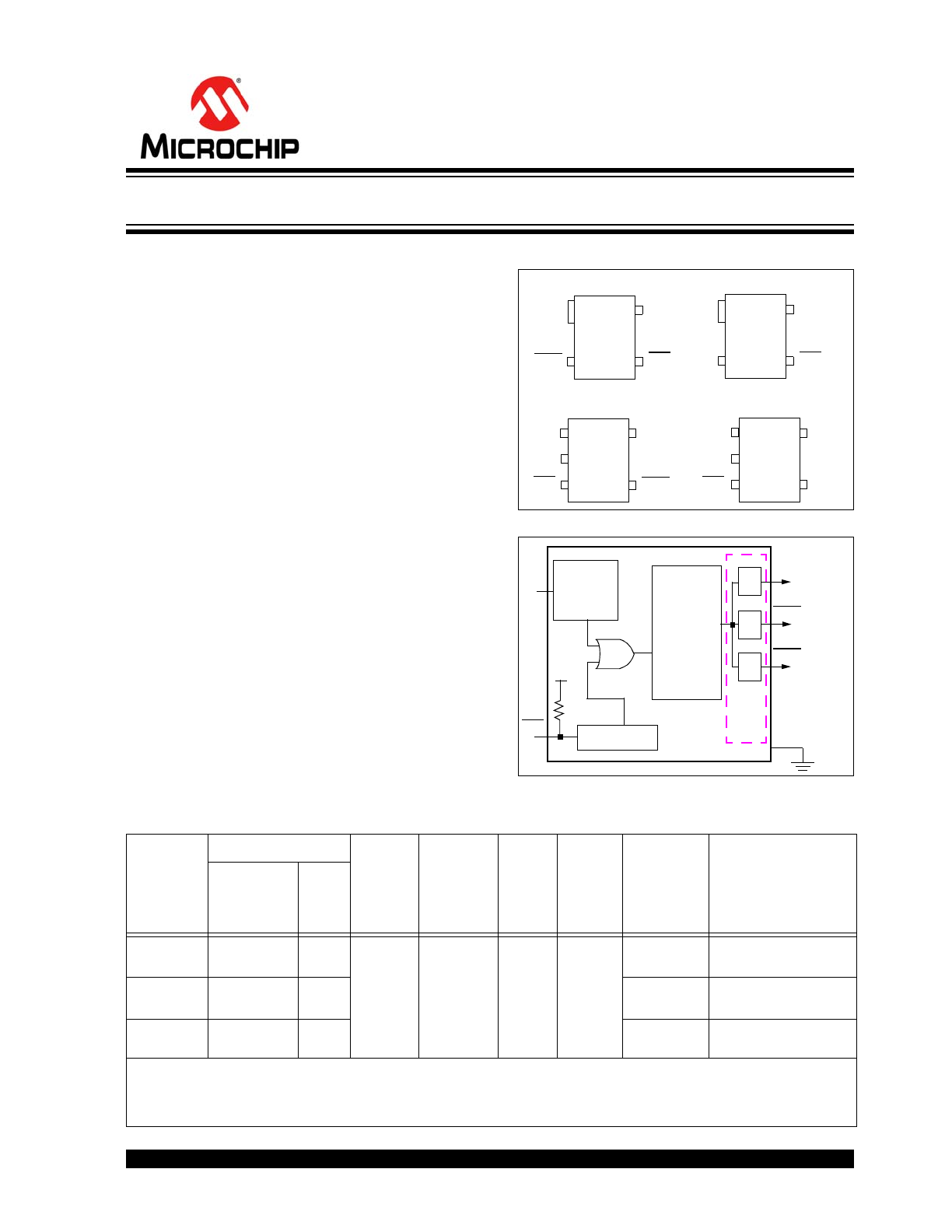
Package Types
Functional Block Diagram
Device Features
1
2
4
3
TC12
71A
SOT-143
V
SS
V
DD
RST
MR
1
2
4
3
TC12
70A
TC12
70
A
N
SOT-143
V
SS
V
DD
RST
MR
1
2
3
5
4
TC
1
271
A
SOT-23-5
1
2
3
5
4
SOT-23-5
NC
NC
V
DD
MR
RST
V
SS
V
SS
V
DD
MR
RST
TC
1
270
A
TC
1
270
A
N
18.5 k
V
DD
MR
RST
RST
Glitch Filter
Voltage
Detector
PP
PP
O
u
tput
Dri
v
e
r
Circuitry
(TC1271A)
(TC1270A)
Reset
Generator
and Delay
Timer
(2.19 ms,
35 ms,
280 ms)
OD
RST
(TC1270AN)
Device
Output
Re
s
e
t De
la
y
(m
s) (
T
y
p
)
(
3
)
R
e
set T
rip
Po
int (V)
(
3
)
Vo
lt
a
g
e
Ra
nge
(V)
T
e
m
p
er
at
u
re
Ra
nge
Packages
Comment
Type
Active
Level
TC1270A
Push-Pull
Low
2.19, 35,
280
(
1
)
4.63, 4.38,
3.08, 2.93,
2.63
(
4
)
1.0V to
5.5V
-40°C to
+125°C
SOT-143
(
2
)
,
SOT-23-5
Replaces TC1270 and
TCM811
TC1270AN Open-Drain
Low
SOT-143
(
2
)
,
SOT-23-5
New Option
TC1271A
Push-Pull
High
SOT-143
(
2
)
,
SOT-23-5
Replaces TC1271 and
TCM812
Note 1:
The 280 ms Reset delay time-out is compatible with the TC1270, TC1271, TCM811 and TCM812 devices.
2:
The SOT-143 package is compatible with the TC1270, TC1271, TCM811 and TCM812 devices.
3:
Custom Reset trip points and Reset delays available, contact your local Microchip sales office.
4:
The TC1270/1 and TCM811/12 1.75V trip point option is not supported.
Voltage Supervisor with Manual Reset Input

TC1270A/70AN/71A
DS22035D-page 2
2007-2011 Microchip Technology Inc.
NOTES:
2007-2011 Microchip Technology Inc.
DS22035D-page 3
TC1270A/70AN/71A
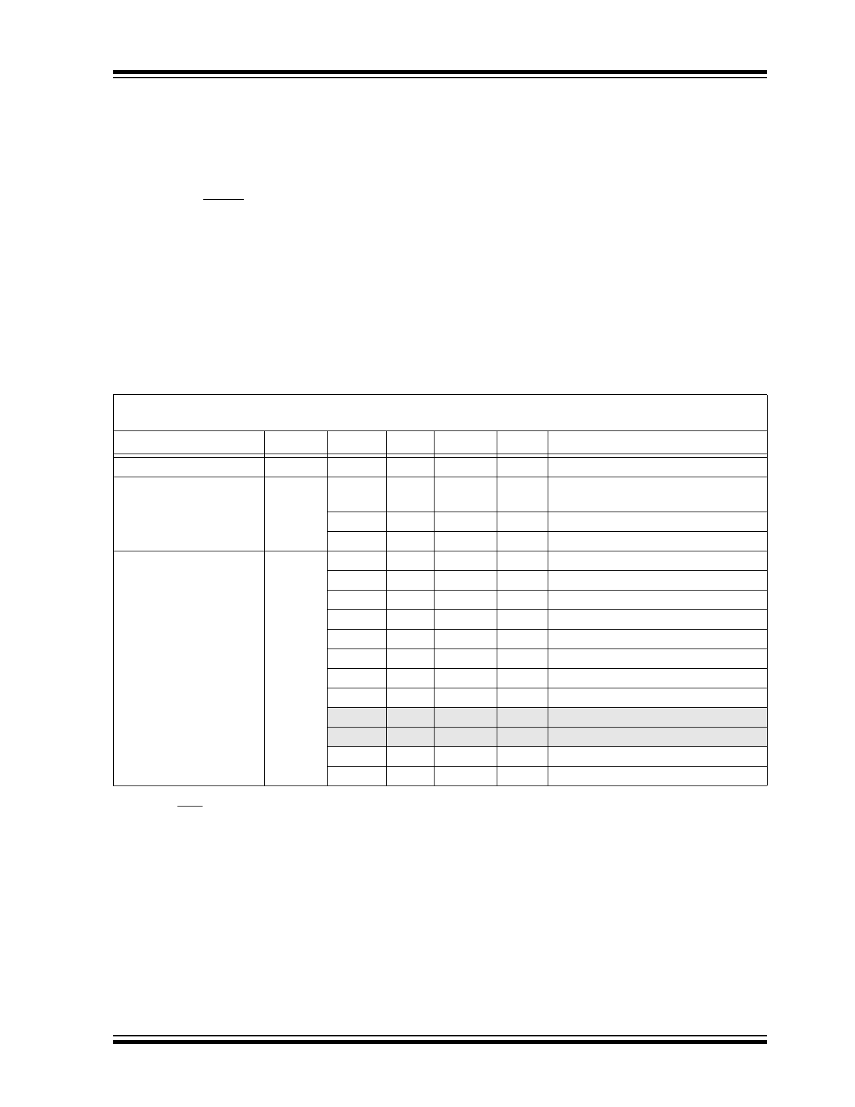
1.0
ELECTRICAL
CHARACTERISTICS
Absolute Maximum Ratings †
Supply Voltage (V
DD
to V
SS
) ............................... +7.0V
Input Current, V
DD
.............................................. 10 mA
Output Current, RESET, Reset .......................... 10 mA
Voltage on all inputs and outputs
w.r.t. V
SS
............................ -0.6V to (V
DD
+ 1.0V)
Storage Temperature Range .............. -65°C to +150°C
Operating Temperature Range .......... -40°C to +125°C
Maximum Junction Temperature, T
S
.................. 150°C
ESD protection on all pins
Human Body Model
4 kV
Machine Model
400V
† Notice: Stresses above those listed under “Absolute
Maximum Ratings” may cause permanent damage to a
device. The absolute maximum values are merely
stress ratings – functional operation of a device at
those, or any other conditions above those indicated in
the operational listing of these specifications, is not
implied. Exposure to absolute maximum rating
conditions for extended periods may affect device
reliability.
ELECTRICAL CHARACTERISTICS
Electrical Characteristics: Unless otherwise noted, V
DD
= 5V for L/M versions, V
DD
= 3.3V for T/S versions,
V
DD
= 3V for R version, T
A
= -40°C to +125°C. Typical values are at T
A
= +25°C.
Parameter
Sym
Min
Typ
(
1
)
Max
Units
Test Conditions
Operating Voltage Range
V
DD
1.0
—
5.5
V
Supply Current
I
DD
—
7
15
µA
V
DD
> V
TRIP
, for L/M/R/S/T,
V
DD
= 5.5V
—
4.75
10
µA
V
DD
> V
TRIP
, for R/S/T, V
DD
= 3.6V
—
10
15
µA
V
DD
< V
TRIP
, for L/M/R/S/T
Reset Trip Point
Threshold
(
3
)
V
TRIP
4.54
4.63
4.72
V
TC127xAL: T
A
= +25°C
4.50
—
4.75
V
T
A
= –40°C to +125°C
4.30
4.38
4.46
V
TC127xAM: T
A
= +25°C
4.25
—
4.50
V
T
A
= –40°C to +125°C
3.03
3.08
3.14
V
TC127xAT: T
A
= +25°C
3.00
—
3.15
V
T
A
= –40°C to +125°C
2.88
2.93
2.98
V
TC127xAS: T
A
= +25°C
2.85
—
3.00
V
T
A
= –40°C to +125°C
2.72
2.77
2.82
V
TC127xA:
(
5
)
T
A
= +25°C
2.70
—
2.85
V
T
A
= –40°C to +125°C
2.58
2.63
2.68
V
TC127xAR: T
A
= +25°C
2.55
—
2.70
V
T
A
= –40°C to +125°C
Note 1:
Data in the Typical (“Typ”) column is at 5V, +25
C, unless otherwise stated.
2:
RST output for TC1270A and TC1270AN, RST output for TC1271A.
3:
TC127XA refers to the TC1270A, TC1270AN or TC1271A device.
4:
Hysteresis is within the V
TRIP(MIN)
to V
TRIP(MAX)
window.
5:
Custom-ordered voltage trip point. Minimum order volume requirement.
6:
This specification allows this device to be used in PIC
®
microcontroller applications that require the
In-Circuit Serial Programming™ (ICSP™) feature (see device-specific programming specifications for
voltage requirements). The total time that the RST pin can be above the maximum device operational
voltage (5.5V) is 100s. Current into the RST pin should be limited to 2 mA. It is recommended that the
device operational temperature be maintained between 0°C to +70°C (+25°C preferred). For additional
information, refer to
Figure 2-41
.
TC1270A/70AN/71A
DS22035D-page 4
2007-2011 Microchip Technology Inc.
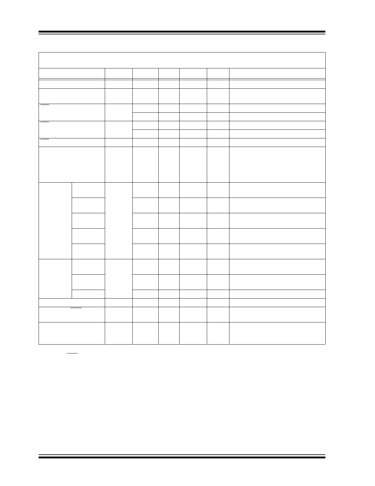
Reset Threshold Tempco
—
±30
—
ppm/°C
Reset Trip Point
Hysteresis
(
1
)
V
HYS
—
0.3
—
%
Percentage of V
TRIP
Voltage
MR Input High Threshold
V
IH
2.3
—
—
V
V
DD
> V
TRIP(MAX)
, L/M only
0.7 V
DD
—
—
V
V
DD
> V
TRIP(MAX)
, R/S/T only
MR Input Low Threshold
V
IL
—
—
0.8
V
V
DD
> V
TRIP(MAX)
, L/M only
—
—
0.25 V
DD
V
V
DD
> V
TRIP(MAX)
, R/S/T only
MR Pull-up Resistance
10
18.5
40
k
Open-Drain High Voltage
on Output
V
ODH
—
—
13.5
V
Open-Drain Output pin only.
V
DD
= 3.0V, Time voltage > 5.5
applied
100s. Current into pin
limited to 2 mA +25°C operation
recommended
(
6
)
Reset
Output
Voltage
Low
(
2
)
TC1270A/
TC1270AN
V
OL
—
—
0.3
V
R/S/T only,
I
SINK
= 1.2 mA, V
DD
= V
TRIP(MIN)
TC1271A
—
—
0.3
V
R/S/T only,
I
SINK
= 1.2 mA, V
DD
= V
TRIP(MAX)
TC1270A/
TC1270AN
—
—
0.4
V
L/M only,
I
SINK
= 3.2 mA, V
DD
= V
TRIP(MIN)
TC1271A
—
—
0.3
V
L/M only,
I
SINK
= 3.2 mA, V
DD
= V
TRIP(MAX)
TC1270A/
TC1270AN
—
—
0.3
V
L/M only,
I
SINK
= 50 µA, V
DD
> 1.0V
Reset
Output
Voltage
High
(
2
)
TC1270A
V
OH
0.8 V
DD
—
—
V
R/S/T
only,
I
SOURCE
= 500 µA, V
DD
= V
TRIP(MAX)
TC1270A
V
DD
- 1.5
—
—
V
L/M only,
I
SOURCE
= 800 µA, V
DD
= V
TRIP(MAX)
TC1271A
0.8 V
DD
—
—
V
I
SOURCE
= 500 µA, V
DD
V
TRIP(MIN)
Input Leakage Current
I
IL
—
—
±1
µA
V
PIN
= V
DD
Open-Drain RST Output
Leakage
I
OLOD
—
—
1
µA
Open-Drain configuration only.
Capacitive Loading
Specification on Output
Pins
C
IO
—
—
50
pF
ELECTRICAL CHARACTERISTICS (CONTINUED)
Electrical Characteristics: Unless otherwise noted, V
DD
= 5V for L/M versions, V
DD
= 3.3V for T/S versions,
V
DD
= 3V for R version, T
A
= -40°C to +125°C. Typical values are at T
A
= +25°C.
Parameter
Sym
Min
Typ
(
1
)
Max
Units
Test Conditions
Note 1:
Data in the Typical (“Typ”) column is at 5V, +25
C, unless otherwise stated.
2:
RST output for TC1270A and TC1270AN, RST output for TC1271A.
3:
TC127XA refers to the TC1270A, TC1270AN or TC1271A device.
4:
Hysteresis is within the V
TRIP(MIN)
to V
TRIP(MAX)
window.
5:
Custom-ordered voltage trip point. Minimum order volume requirement.
6:
This specification allows this device to be used in PIC
®
microcontroller applications that require the
In-Circuit Serial Programming™ (ICSP™) feature (see device-specific programming specifications for
voltage requirements). The total time that the RST pin can be above the maximum device operational
voltage (5.5V) is 100s. Current into the RST pin should be limited to 2 mA. It is recommended that the
device operational temperature be maintained between 0°C to +70°C (+25°C preferred). For additional
information, refer to
Figure 2-41
.
2007-2011 Microchip Technology Inc.
DS22035D-page 5
TC1270A/70AN/71A
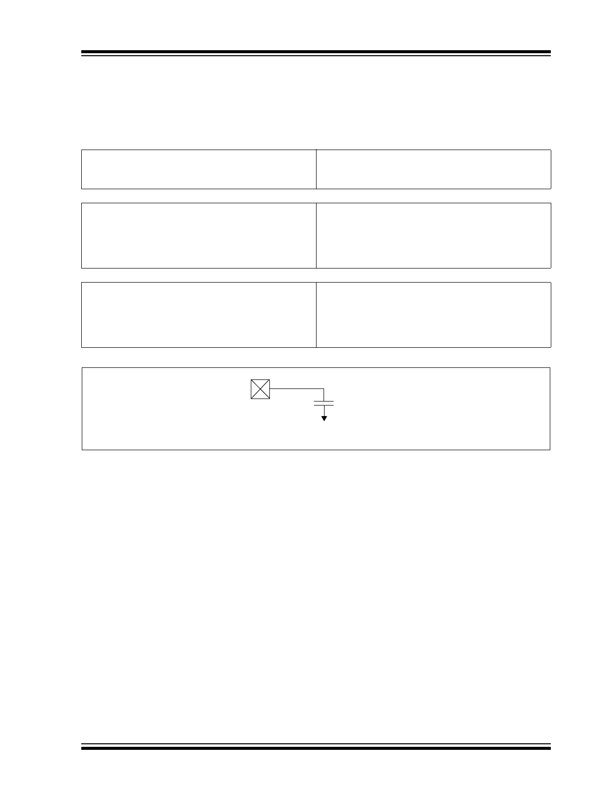
1.1
AC CHARACTERISTICS
1.1.1
TIMING PARAMETER SYMBOLOGY
The timing parameter symbols have been created
following one of the following formats:
FIGURE 1-1:
Test Load Conditions.
1. TppS2ppS
2. TppS
T
F
Frequency
T
Time
E
Error
Lowercase letters (pp) and their meanings:
pp
io
Input or Output pin
osc
Oscillator
rx
Receive
tx
Transmit
bitclk
RX/TX BITCLK
RST
Reset
drt
Device Reset Timer
Uppercase letters and their meanings:
S
F
Fall
P
Period
H
High
R
Rise
I
Invalid (High-impedance)
V
Valid
L
Low
Z
High-impedance
Pin
V
SS
C
L
= 50 pF
TC1270A/70AN/71A
DS22035D-page 6
2007-2011 Microchip Technology Inc.
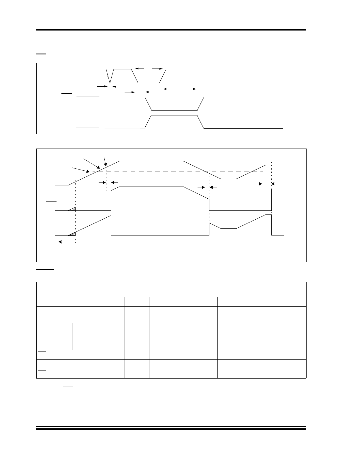
TIMING DIAGRAMS AND SPECIFICATIONS
MR Pin and Reset Pin Waveform
Device Voltage and Reset Pin (Active Low) Waveform
Reset and Device Reset Timer Requirements
Electrical Characteristics: Unless otherwise noted, V
DD
= 5V for L/M versions, V
DD
= 3.3V for T/S versions,
V
DD
= 3V for R version, T
A
= -40°C to +125°C. Typical values are at T
A
= +25°C.
Parameter
Sym
Min
Typ
(
1
)
Max
Units
Test Conditions
V
DD
to Reset Delay
t
RD
—
50
—
µs
V
DD
= V
TRIP(MAX)
to
V
TRIP(MIN)
–125 mV
Reset Active
Time Out
Period
TC127XAxBVyy
(
3
)
t
RST
1.09
2.19
4.38
ms
V
DD
= V
TRIP(MAX)
TC127XAxAVyy
(
3
)
17.5
35
70
ms
V
DD
= V
TRIP(MAX)
TC127XAxVyy
(
3
)
140
280
560
ms
V
DD
= V
TRIP(MAX)
MR Minimum Pulse Width
t
MR
10
—
—
µs
MR Noise Immunity
t
MRNI
—
0.1
—
µs
MR to Reset Propagation Delay
t
MD
—
0.2
—
µs
Note 1:
Unless otherwise stated, data in the Typical (“Typ”) column is at 5V, +25
C.
2:
RST output for TC1270A, RST output for TC1271A.
3:
TC127XA refers to the TC1270A, TC1270AN or TC1271A device.
“x” indicates the selected voltage trip point, while “yy” indicates the package code.
MR
RST
t
RST
t
MR
RST
t
MD
t
MRNI
V
TRIP(MAX)
V
TRIP(MIN)
1V
V
DD
V
TRIP
t
RST
RST
(1)
RST
t
RST
t
RD
V
DD
< 1V is outside the device operating specification. The RST (or RST) output state is unknown while V
DD
< 1V.
Note 1:
The TC1270AN requires an external pull-up resistor.
2007-2011 Microchip Technology Inc.
DS22035D-page 7
TC1270A/70AN/71A
TEMPERATURE CHARACTERISTICS
Electrical Specifications: Unless otherwise indicated, V
DD
= +1.0V to +5.5V, V
SS
= GND.
Parameters
Sym
Min
Typ
Max
Units
Conditions
Temperature Ranges
Specified Temperature Range
T
A
-40
—
+125
°C
Operating Temperature Range
T
A
-40
—
+125
°C
Storage Temperature Range
T
A
-65
—
+150
°C
Thermal Package Resistances
Thermal Resistance, 5L-SOT-23
JA
—
256
—
°C/W
Thermal Resistance, 4L-SOT-143
JA
—
426
—
°C/W

TC1270A/70AN/71A
DS22035D-page 8
2007-2011 Microchip Technology Inc.
NOTES:
2007-2011 Microchip Technology Inc.
DS22035D-page 9
TC1270A/70AN/71A
2.0
TYPICAL PERFORMANCE CURVES
Note: Unless otherwise indicated, all limits are specified for V
DD
= 1V to 5.5V, T
A
= –40°C to +125°C.
FIGURE 2-1:
I
DD
vs. Temperature (Reset
Power-up Timer Inactive)
(TC1270AL, TC1270ANL, TC1271AL
- 4.50V min./4.63V typ./4.75V max.).
FIGURE 2-2:
I
DD
vs. Temperature (Reset
Power-up Timer Inactive)
(TC1270AT, TC1270ANT, TC1271AT
- 3.00V min./3.08V typ./3.15V max.).
FIGURE 2-3:
I
DD
vs. Temperature (Reset
Power-up Timer Inactive)
(TC1270AR, TC1270ANR, TC1271AR
- 2.55V min./2.63V typ./2.70V max.).
FIGURE 2-4:
I
DD
vs. Temperature (Reset
Power-up Timer Active)
(TC1270AL, TC1270ANL, TC1271AL
- 4.50V min./4.63V typ./4.75V max.).
FIGURE 2-5:
I
DD
vs. Temperature (Reset
Power-up Timer Active)
(TC1270AT, TC1270ANT, TC1271AT
- 3.00V min./3.08V typ./3.15V max.).
FIGURE 2-6:
I
DD
vs. Temperature (Reset
Power-up Timer Active)
(TC1270AR, TC1270ANR, TC1271AR
- 2.55V min./2.63V typ./2.70V max.).
Note:
The graphs and tables that follow this note are the result of a statistical summary based on a limited number
of samples and are provided for informational purposes only. The performance characteristics listed herein
are not tested or guaranteed. In some graphs or tables, the data presented may be outside the specified
operating range (e.g., outside specified power supply range) and therefore outside the warranted range.
0
0.5
1
1.5
2
2.5
-40
-20
0
20
40
60
80
100
120
Temperature (°C)
I
DD
(µ
A
)
1.0V
2.0V
3.0V
4.0V
5.0V
0
0.5
1
1.5
2
2.5
3
-4
0
-2
0
0
20
40
60
80
10
0
12
0
Temperature (°C)
I
DD
(µA)
1.0V
2.0V
3.0V
4.0V
5.0V
0
0.5
1
1.5
2
2.5
3
-4
0
-2
0
0
20
40
60
80
10
0
12
0
Temperature (°C)
I
DD
(µ
A
)
1.0V
2.0V
3.0V
4.0V
5.0V
4.5
5
5.5
6
6.5
7
-4
0
-2
0
0
20
40
60
80
10
0
12
0
Temperature (°C)
I
DD
(µA)
4.8V
5.5V
3
3.5
4
4.5
5
5.5
6
6.5
7
-4
0
-2
0
0
20
40
60
80
10
0
12
0
Temperature (°C)
I
DD
(µA)
4.5V
5.5V
3.5V
2.5
3
3.5
4
4.5
5
5.5
6
6.5
-4
0
-2
0
0
20
40
60
80
10
0
12
0
Temperature (°C)
I
DD
(µA)
4.0V
5.0V
3.0V
TC1270A/70AN/71A
DS22035D-page 10
2007-2011 Microchip Technology Inc.
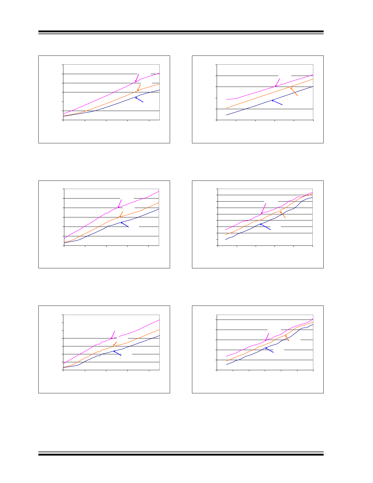
Note: Unless otherwise indicated, all limits are specified for V
DD
= 1V to 5.5V, T
A
= –40°C to +125°C.
FIGURE 2-7:
I
DD
vs. V
DD
(Reset
Power-up Timer Inactive)
(TC1270AL, TC1270ANL, TC1271AL
- 4.50V min./4.63V typ./4.75V max.).
FIGURE 2-8:
I
DD
vs. V
DD
(Reset
Power-up Timer Inactive)
(TC1270AT, TC1270ANT, TC1271AT
- 3.00V min./3.08V typ./3.15V max.).
FIGURE 2-9:
I
DD
vs. V
DD
(Reset
Power-up Timer Inactive)
(TC1270AR, TC1270ANR, TC1271AR
- 2.55V min./2.63V typ./2.70V max.).
FIGURE 2-10:
I
DD
vs. V
DD
(Reset
Power-up Timer Active)
(TC1270AL, TC1270ANL, TC1271AL
- 4.50V min./4.63V typ./4.75V max.).
FIGURE 2-11:
I
DD
vs. V
DD
(Reset
Power-up Timer Active)
(TC1270AT, TC1270ANT, TC1271AT
- 3.00V min./3.08V typ./3.15V max.).
FIGURE 2-12:
I
DD
vs. V
DD
(Reset
Power-up Timer Active)
(TC1270AR, TC1270ANR, TC1271AR
- 2.55V min./2.63V typ./2.70V max.).
0
0.5
1
1.5
2
2.5
3
1
2
3
4
5
V
DD
(V)
I
DD
(µ
A
)
-40°C
+125°C
+25°C
0
0.5
1
1.5
2
2.5
3
1
2
3
4
5
V
DD
(V)
I
DD
(µ
A
)
-40°C
+125°C
+25°C
0
0.5
1
1.5
2
2.5
3
3.5
1
2
3
4
5
V
DD
(V)
I
DD
(µA)
-40°C
+125°C
+25°C
4.5
5
5.5
6
6.5
7
4.5
4.7
4.9
5.1
5.3
5.5
V
DD
(V)
I
DD
(µA)
-40°C
+125°C
+25°C
2.5
3
3.5
4
4.5
5
5.5
6
6.5
7
3
3.5
4
4.5
5
5.5
V
DD
(V)
I
DD
(µ
A
)
-40°C
+125°C
+25°C
2
3
4
5
6
7
2.5
3
3.5
4
4.5
5
5.5
V
DD
(V)
I
DD
(µA)
-40°C
+125°C
+25°C