
© 2007 Microchip Technology Inc.
DS21381D-page 1
TC1270/TC1271
Features:
• Precision V
CC
Monitor for 1.8V, 2.7V, 3.0V, 3.3V
and 5.0V Nominal Supplies
• Manual Reset Input
• 140 ms Minimum RESET, Reset Output Duration
• RESET Output Valid to V
CC
= 1.0V (TC1270)
• Low 7 µA Supply Current
• V
CC
Transient Immunity
• Small 4-Pin SOT-143 Package
• No External Components
• Replacement for MAX811/812 and Offers a Lower
Threshold Voltage Option
Applications:
• Computers
• Embedded Systems
• Battery Powered Equipment
• Critical µP Power Supply Monitoring
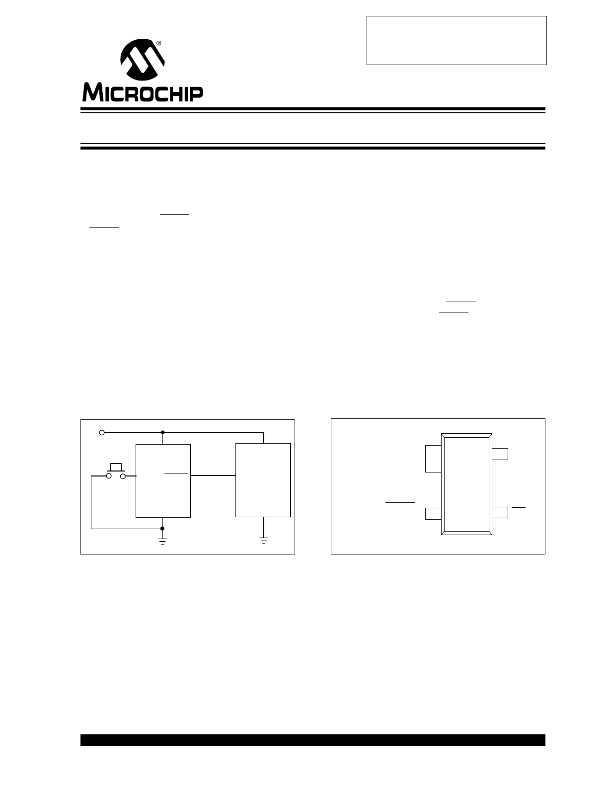
Typical Operating Circuit
General Description
The TC1270 and TC1271 are cost-effective system
supervisor circuits designed to monitor V
CC
in digital
systems and provide a reset signal to the host
processor when necessary. A manual reset input is
provided to override the reset monitor, and is suitable
for use as a push button reset. No external components
are required.
The reset output is driven active within 20 µs (4 µs for
F version) of V
CC
falling through the reset voltage
threshold. Reset is maintained active for a minimum of
140 ms after V
CC
rises above the reset threshold. The
TC1271 has an active-high RESET output while the
TC1270 has an active-low RESET output. The output
of the TC1270 is valid down to V
CC
= 1V. Both devices
are available in a 4-Pin SOT-143 package.
The TC1270/TC1271 devices are optimized to reject
fast transient glitches on the V
CC
line. Low supply
current of 7 µA (V
CC
= 3.3V) makes these devices
suitable for battery powered applications.
Package Type
TC1270
V
CC
V
CC
V
CC
RESET
Reset
Input
(Active Low)
GND
GND
Processor
MR
Push
Button
V
CC
TC1270 RESET
GND
TC1270
TC1271
1
2
TC1271 (RESET)
3
4
MR
4-Pin Reset Monitors
Obsolete Device
Recommended Replacements:
TC1270A, TC1270AN, TC1271A
TC1270/TC1271
DS21381D-page 2
© 2007 Microchip Technology Inc.
1.0
ELECTRICAL
CHARACTERISTICS
Absolute Maximum Ratings†
Supply Voltage (V
CC
to GND) .............................+6.0V
RESET, Reset ............................ -0.3V to (V
CC
+ 0.3V)
Input Current, V
CC
..............................................20 mA
Output Current, RESET, Reset...........................20 mA
Operating Temperature Range............. -40°C to +85°C
Storage Temperature Range ..............-65°C to +150°C
† Stresses above those listed under “Absolute
Maximum Ratings” may cause permanent damage to
the device. These are stress ratings only and functional
operation of the device at these or any other conditions
above those indicated in the operation sections of the
specifications is not implied. Exposure to Absolute
Maximum Rating conditions for extended periods may
affect device reliability.
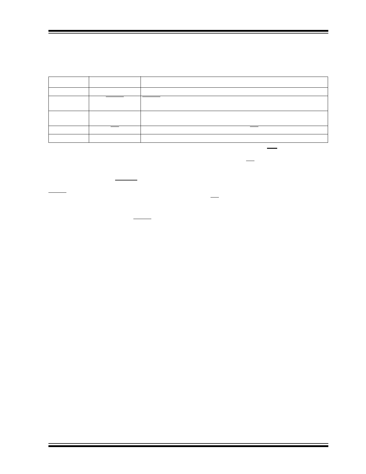
ELECTRICAL SPECIFICATIONS
Electrical Characteristics: V
CC
= 5V for L/M versions, V
CC
= 3.3V for T/S versions, V
CC
= 3V for R version, V
CC
= 2.0V for F
version. Unless otherwise noted, T
A
= -40°C to +85°C. Typical values are at T
A
= +25°C. (Note 1).
Symbol
Parameter
Min
Typ
Max
Units
Test Conditions
V
CC
V
CC
Range
1.2
—
5.5
V
I
CC
Supply Current
—
7
15
µA
V
CC
> V
TH
, for L/M/R/S/T/F
—
10
15
µA
V
CC
< V
TH
, for L/M/R/S/T
—
6
12
µA
V
CC
< V
TH
, for F
V
TH
Reset Threshold
4.54
4.50
4.63
—
4.72
4.75
V
V
TC127_L; T
A
= +25°C
T
A
= -40°C to +85°C
4.30
4.25
4.38
—
4.46
4.50
V
V
TC127_M; T
A
= +25°C
T
A
= -40°C to +85°C
3.03
3.00
3.08
—
3.14
3.15
V
V
TC127_T; T
A
= +25°C
T
A
= -40°C to +85°C
2.88
2.85
2.93
—
2.98
3.00
V
V
TC127_S; T
A
= +25°C
T
A
= -40°C to +85°C
2.58
2.55
2.63
—
2.68
2.70
V
V
TC127_R; T
A
= +25°C
T
A
= -40°C to +85°C
1.71
1.70
1.75
—
1.79
1.80
V
V
TC127_F; T
A
= +25°C
T
A
= -40°C to +85°C
Reset Threshold Tempco
—
30
—
ppm/°C
V
CC
to Reset Delay
—
—
20
5
—
—
µs
V
CC
= V
TH
to V
TH
– 125 mV;
L/M/R/S/T/F
t
RP
Reset Active Time-out Period
140
280
560
ms
V
CC
= V
TH(MAX)
t
MR
MR Minimum Pulse Width
10
—
—
µs
MR Glitch Immunity
—
0.1
—
µs
t
MD
MR to Reset Propagation Delay
—
0.5
—
µs
V
IH
MR Input Threshold
2.3
—
—
V
V
CC
> V
TH(MAX)
, TC127_L/M
0.7 V
CC
—
—
V
V
CC
> V
TH(MAX)
, TC127_R/S/T/F
V
IL
—
—
0.8
V
V
CC
> V
TH(MAX)
, TC127_L/M
—
—
0.15 V
CC
V
V
CC
> V
TH(MAX)
, TC127_R/S/T/F
MR Pull-up Resistance
10
20
40
k
Ω
V
OH
Reset Output Voltage High
(TC1271)
0.8 V
CC
—
—
V
I
SOURCE
= 150 µA;
V
CC
≤ V
TH(MIN)
Note
1:
Production testing done at T
A
= +25°C, over temperature limits ensured by design.
2:
RESET output for TC1270, Reset output for TC1271.
© 2007 Microchip Technology Inc.
DS21381D-page 3
TC1270/TC1271
V
OL
Reset Output Voltage Low
(TC1271)
—
—
0.2
V
TC1271F only,
I
SINK
= 500 µA,
V
CC
= V
TH(MAX)
—
—
0.3
V
TC1271R/S/T only,
I
SINK
= 1.2 mA, V
CC
= V
TH(MAX)
—
—
0.4
V
TC1271L/M only, I
SINK
= 3.2 mA,
V
CC
= V
TH(MAX)
V
OL
RESET Output Voltage Low
(TC1270)
—
—
0.3
V
TC1270R/S/T only,
I
SINK
= 1.2 mA, V
CC
= V
TH(MIN)
TC1270F only:
I
SINK
= 500 µA, V
CC
= V
TH(MIN)
—
—
—
—
0.4
TBD
V
V
TC1270L/M only,
I
SINK
= 3.2 mA, V
CC
= V
TH(MIN)
I
SINK
= 50 µA, V
CC
> 1.0V
V
OH
RESET Output Voltage High
(TC1270)
V
CC
– 1.5
—
—
V
TC1270L/M only,
I
SOURCE
= 800 µA,
V
CC
= V
TH(MAX)
0.8 V
CC
—
—
V
TC1270R/S/T/F only,
I
SOURCE
= 500 µA,
V
CC
= V
TH(MAX)
ELECTRICAL SPECIFICATIONS (CONTINUED)
Electrical Characteristics: V
CC
= 5V for L/M versions, V
CC
= 3.3V for T/S versions, V
CC
= 3V for R version, V
CC
= 2.0V for F
version. Unless otherwise noted, T
A
= -40°C to +85°C. Typical values are at T
A
= +25°C. (Note 1).
Symbol
Parameter
Min
Typ
Max
Units
Test Conditions
Note
1:
Production testing done at T
A
= +25°C, over temperature limits ensured by design.
2:
RESET output for TC1270, Reset output for TC1271.
TC1270/TC1271
DS21381D-page 4
© 2007 Microchip Technology Inc.
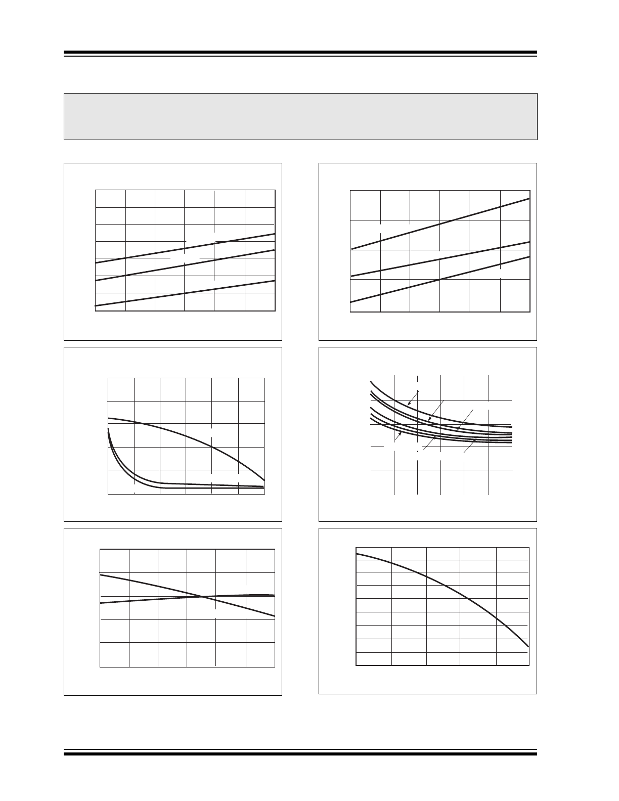
2.0
TYPICAL CHARACTERISTICS
Note:
The graphs and tables provided following this note are a statistical summary based on a limited number of
samples and are provided for informational purposes only. The performance characteristics listed herein
are not tested or guaranteed. In some graphs or tables, the data presented may be outside the specified
operating range (e.g., outside specified power supply range) and therefore outside the warranted range.
V
CC
= 1V
TEMPERATURE (°C)
8
10
12
14
6
4
2
0
-40
0
20
-20
40
60
85
SUPPL
Y
CURRENT (
μ
A)
Supply Current vs.Temperature
(No Load, TC127xR/S/T/F)
V
CC
= 5V
V
CC
= 3V
TEMPERATURE (°C)
30
40
50
20
10
0
-40
0
20
-20
40
60
85
POWER-DOWN RESET DELA
Y
(
μ
sec)
Power-Down Reset Delay vs. Temperature
(TC127xF)
V
OD
= 20mV
V
OD
= 100mV
V
OD
= 200 mV
TEMPERATURE (°C)
240
245
250
235
230
225
-40
0
20
-20
40
60
85
POWER-UP
RESET TIMEOUT (msec)
Power-Up Reset Time-out vs. Temperature
TC127xL/M
TC127xR/S/T/F
8
6
4
2
0
TEMPERATURE (°C)
-40
0
20
-20
40
60
85
SUPPL
Y
CURRENT (
μ
A)
Supply Current vs.Temperature
(No Load, TC127xL/M)
V
CC
= 5V
V
CC
= 3V
V
CC
= 1V
L/M
R/S/T
TEMPERATURE (°C)
30
40
50
20
10
0
-40
0
20
-20
40
60
85
POWER-DOWN RESET DELA
Y
(
μ
sec)
Power-Down Reset Delay vs. Temperature
(TC127xL/M/R/S/T)
V
OD
= 20 mV
V
OD
= 20 mV
V
OD
= 100 mV
V
OD
= 200 mV
V
OD
= 100 mV
V
OD
= 200 mV
1.0010
1.0020
1.0030
1.0000
0.9990
0.9980
0.9970
0.9960
0.9950
0.9940
TEMPERATURE (°C)
-40
10
35
-15
65
60
NORMALIZED THRESHOLD (V)
Normalized Reset Threshold vs. Temperature
© 2007 Microchip Technology Inc.
DS21381D-page 5
TC1270/TC1271
3.0
PIN DESCRIPTIONS
The descriptions of the pins are listed in
Table 3-1
.
TABLE 3-1:
PIN FUNCTION TABLE
3.1
Ground Terminal (GND)
GND provides the negative reference for the analog
input voltage. Typically, the circuit ground is used.
3.2
Reset Output (RESET) (TC1270)
RESET output remains low while V
CC
is below the
Reset voltage threshold (V
TRIP
). Once the device
voltage (V
CC
) returns to a high level (V
TRIP
+ V
HYS
), the
device will remain in Reset for the Reset delay timer
(T
RST
). After that time expires, the RESET pin will be
driven to the high state.
3.3
Reset Output (RESET) (TC1271)
RESET output remains high while V
CC
is below the
Reset voltage threshold (V
TRIP
). Once the device
voltage (V
CC
) returns to a high level (V
TRIP
+ V
HYS
), the
device will remain in Reset for the Reset delay timer
(T
RST
). After that time expires, the RESET pin will be
driven to the low state.
3.4
Manual Reset (MR)
The Manual Reset (MR) input pin allows a push button
switch to easily be connected to the system. When the
push button is depressed, it forces a system Reset.
This pin has circuitry that filters noise that may be pres-
ent on the MR signal.
The MR pin is active-low and has an internal pull-up
resistor.
3.5
Supply Voltage (V
CC
)
V
CC
can be used for power supply monitoring or a
voltage level that requires monitoring.
Pin No.
Symbol
Description
1
GND
Ground
2
RESET
(
TC1270)
RESET output remains low while V
CC
is below the Reset voltage threshold,
and for at least 140 ms min. after
V
CC
rises above Reset threshold
2
RESET
(TC1271)
Reset output remains high while V
CC
is below the Reset voltage threshold,
and for at least 140 ms min. after
V
CC
rises above Reset threshold
3
MR
Manual Reset input generates a Reset when MR is below V
IL
4
V
CC
Supply voltage
TC1270/TC1271
DS21381D-page 6
© 2007 Microchip Technology Inc.
4.0
APPLICATIONS INFORMATION
4.1
V
CC
Transient Rejection
The TC1270/TC1271 provides accurate V
CC
monitoring and Reset timing during power-up,
power-down, and brownout/sag conditions, and rejects
negative-going transients (glitches) on the power
supply line.
Figure 4-3
shows the maximum transient
duration vs. maximum negative excursion (overdrive)
for glitch rejection. Any combination of duration and
overdrive that lays under the curve will not generate a
Reset signal. Combinations above the curve are
detected as a brown-out or power-down. Transient
immunity can be improved by adding a capacitor in
close proximity to the V
CC
pin of the TC1270/TC1271.
FIGURE 4-1:
Maximum Transient
Duration vs. Overdrive for Glitch Rejection at
+25°C.
4.2
Reset Signal Integrity During
Power-Down
The TC1270 RESET output is valid to V
CC
= 1.0V.
Below this voltage the output becomes an “open circuit”
and does not sink current. This means CMOS logic
inputs to the microprocessor will be floating at an
undetermined voltage. Most digital systems are
completely shut down well above this voltage.
However, in situations where RESET must be
maintained valid to V
CC
= 0V, a pull-down resistor must
be connected from RESET to ground to discharge stray
capacitances and hold the output low (
Figure 4-2
). This
resistor value, though not critical, should be chosen
such that it does not appreciably load RESET under
normal operation (100 k
Ω will be suitable for most
applications). Similarly, a pull-up resistor to V
CC
is
required for the TC1271 to ensure a valid high RESET
for V
CC
below 1.1V.
FIGURE 4-2:
Ensuring RESET Valid to
V
CC
= 0V.
4.3
Processors With Bidirectional
I/O Pins
Some microprocessors (such as Motorola’s 68HC11)
have bidirectional Reset pins. Depending on the
current drive capability of the processor pin, an indeter-
minate logic level may result if there is a logic conflict.
This can be avoided by adding a 4.7 k
Ω resistor in
series with the output of the TC1270/TC1271
(
Figure 4-3
). If there are other components in the sys-
tem which require a Reset signal, they should be buff-
ered so as not to load the Reset line. If the other
components are required to follow the Reset I/O of the
microprocessor, the buffer should be connected as
shown with the solid line.
FIGURE 4-3:
Interfacing to Bidirectional
Reset I/O.
RESET COMPARATOR OVERDRIVE,
V
TH
- V
CC
(mV)
400
240
160
320
80
0
1
10
100
1000
MAXIMUM TRANSIENT DURA
TION (msec)
T
A
= +25°C
V
TH
Duration
Overdrive
V
CC
TC127LMJ
TC127xR/S/T
TC1270
V
CC
V
CC
R1
100k
RESET
GND
TC1270
V
CC
RESET
GND
RESET
GND
Buffered RESET
To Other System
Components
Buffer
μ
P
4.7k
V
CC
V
CC
© 2007 Microchip Technology Inc.
DS21381D-page 7
TC1270/TC1271
5.0
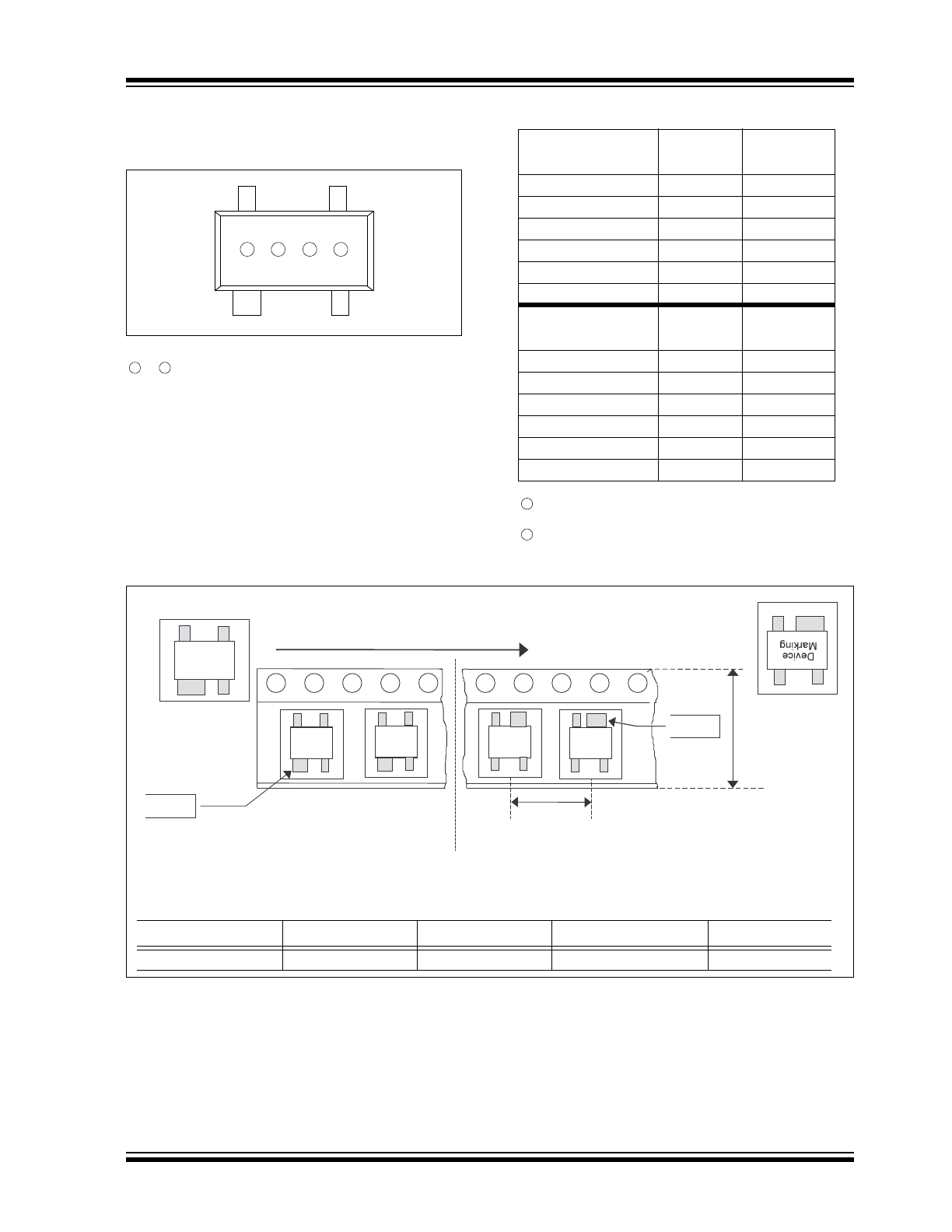
PACKAGING INFORMATION
5.1
Package Marking Information
5.2
Taping Form
1
1
2
3
4
1
&
= part number code + threshold voltage
2
(two-digit code)
Part Number
(V)
TC1270
Code
TC1270LERCTR
4.63
S1
TC1270MERCTR
4.38
S2
TC1270TERCTR
3.08
S3
TC1270SERCTR
2.93
S4
TC1270RERCTR
2.63
S5
TC1270FERCTR
1.75
S7
Part Number
(V)
TC1271
Code
TC1271LERC
TR
4.63
T1
TC1271MERC
TR
4.38
T2
TC1271TERC
TR
3.08
T3
TC1271SERC
TR
2.9
T4
TC1271RERC
TR
2.63
T5
TC1271FERC
TR
1.75
T7
3
represents year and quarter code
4
represents production lot ID code
Device
Marking
P, Pitch
W, Width
of Carrier
Tape
User Direction of Feed
Pin 1
Standard Reel Component Orientation
Reverse Reel Component Orientation
Pin 1
for TR Suffix Device
(Mark Right Side Up)
Package
Carrier Width (W)
Pitch (P)
Part Per Full Reel
Reel Size
4-Pin SOT-143
8 mm
4 mm
3000
7 in.
TC1270/TC1271
DS21381D-page 8
© 2007 Microchip Technology Inc.
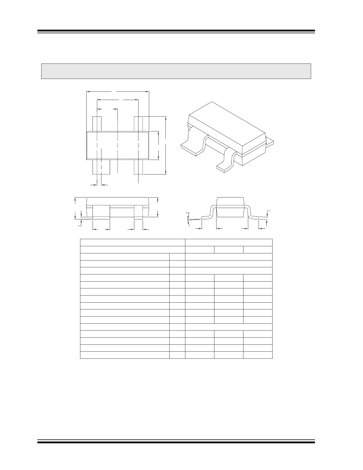
4-Lead Plastic Small Outline Transistor (RC) [SOT-143]
Notes:
1. § Significant Characteristic.
1. Dimensions D and E1 do not include mold flash or protrusions. Mold flash or protrusions shall not exceed 0.25 mm per side.
2. Dimensioning and tolerancing per ASME Y14.5M.
BSC: Basic Dimension. Theoretically exact value shown without tolerances.
REF: Reference Dimension, usually without tolerance, for information purposes only.
Note:
For the most current package drawings, please see the Microchip Packaging Specification located at
http://www.microchip.com/packaging
Units
MILLIMETERS
Dimension Limits
MIN
NOM
MAX
Number of Pins
N
4
Pitch
e
1.92 BSC
Pin1 Offset
e1
0.20 BSC
Overall Height
A
0.80
–
1.22
Molded Package Thickness
A2
0.75
0.90
1.07
Standoff §
A1
0.01
–
0.15
Overall Width
E
2.10
–
2.64
Molded Package Width
E1
1.20
1.30
1.40
Overall Length
D
2.67
2.90
3.05
Foot Length
L
0.13
0.50
0.60
Footprint
L1
0.54 REF
Foot Angle
φ
0°
–
8°
Lead Thickness
c
0.08
–
0.20
Lead 1 Width
b1
0.76
–
0.94
Leads 2, 3 & 4 Width
b
0.30
–
0.54
D
e
e/2
N
E
E1
2
1
e1
A
A1
b2
A2
3X
b
c
L
L1
φ
Microchip Technology Drawing C04-031B

© 2007 Microchip Technology Inc.
DS21381D-page 9
TC1270/TC1271
APPENDIX A:
REVISION HISTORY
Revision D (February 2007)
• Section 5.0 “Packaging Information”:
Corrected SOT-143 Packaging Information.
• Section 3.0 “Pin Descriptions”: Added pin
descriptions.
• Added disclaimer on package outline drawing.
• Updated package outline drawing.
• Section 1.0 “Electrical Characteristics”: Refo-
matted table.
Revision C (June 2006)
• Enhanced SOT-143 Packaging Information.
Revision B (May 2002)
• Undocumented changes.
Revision A (March 2002)
• Original Release of this Document.

TC1270/TC1271
DS21381D-page 10
© 2007 Microchip Technology Inc.
NOTES: