
2001-2014 Microchip Technology Inc.
DS20001377D-page 1
TC1266
Features:
• Glitch Free Transition Between Input Sources
• Automatic Input Source Selection
• External PMOS Bypass Switch Control
• Built-in 5V Detector
• 1% Regulated Output Voltage Accuracy
• 200mA Load Current Capability
• Kelvin Sense Input
• Low Dropout Voltage (240mV @ Full Load)
• Low Ground Current, Independent of Load
Applications:
• PCMCIA
• PCI
• Network Interface Cards (NICs)
• Cardbus
TM
Technology
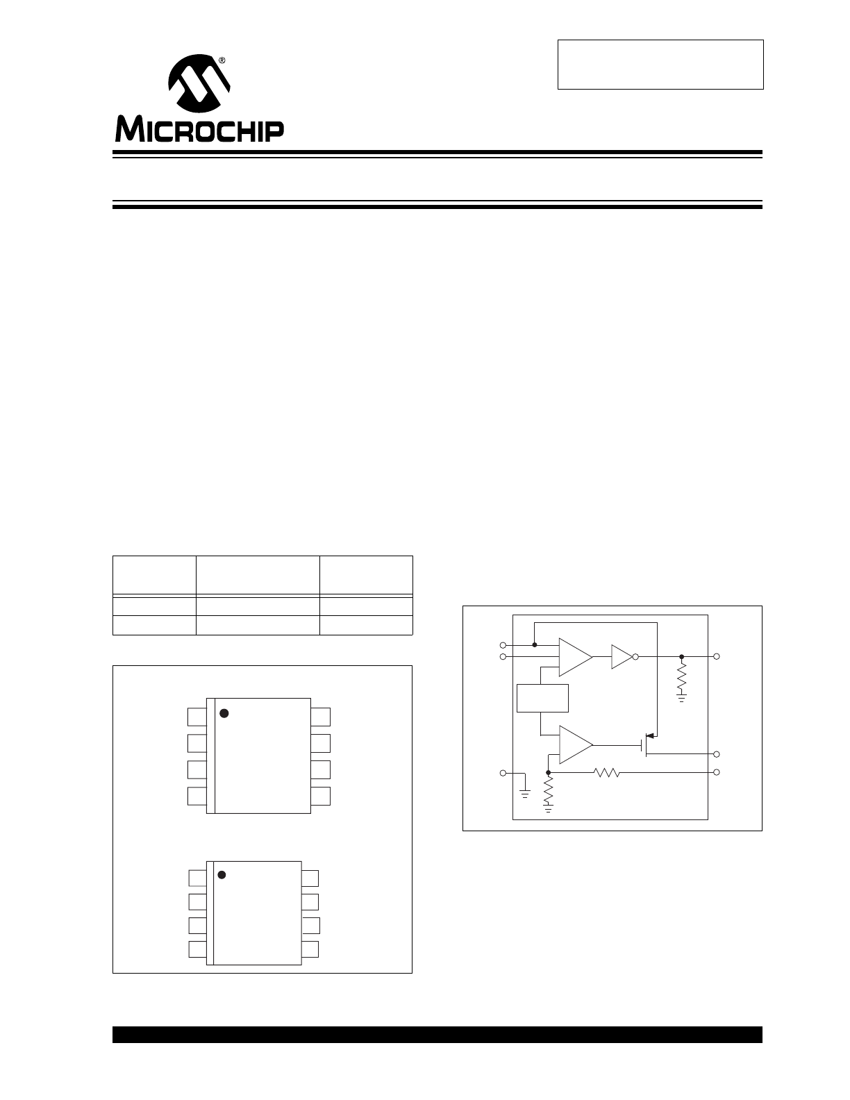
Device Selection Table
Package Type
General Description:
The TC1266 is an application-specific, low dropout
regulator (LDO), specifically intended for use in PCI
peripheral card applications complying with PCI Power
Management (PCI 2.0). It provides an uninterrupted,
3.3V, 200mA (max) output voltage when the main (5V)
or auxiliary (3.3V) input voltage supplies are present.
The TC1266 consists of an LDO, a voltage threshold
detector, external switchover logic and gate drive
circuitry. It functions as a conventional LDO as long as
the voltage on the main supply input (V
IN
) is above the
lower threshold (3.90V typical). Should the voltage on
V
IN
fall below the lower threshold, the LDO is disabled
and an external P-channel MOSFET is automatically
turned on, connecting the auxiliary supply input to
V
OUT,
and ensuring an uninterrupted 3.3V output. The
main supply is automatically selected, if both the main
and auxiliary input supplies are present, and transition
from one input supply to the other is ensured glitch-
free. High integration, automatic secondary supply swi-
tchover, Kelvin sensing, and small size make the
TC1266 the optimum LDO for PCI 2.0 applications.
Functional Block Diagram
Part Number
Package
Junction
Temp. Range
TC1266VOA 8-Pin SOIC (Narrow) -5°C to +125°C
TC1266VUA
8-Pin MSOP
-5°C to +125°C
1
2
3
4
8
7
6
5
TC1266
SENSE
V
OUT
NC
8-Pin SOIC
NC
V
AUX
GND
V
IN
D
R
1
2
3
4
8
7
6
5
TC1266
8-Pin MSOP
NC
V
AUX
GND
V
IN
SENSE
V
OUT
NC
D
R
+
–
V
IN
V
AUX
GND
D
R
V
OUT
SENSE
Bandgap
Reference
Detect
E/A
200mA PCI LDO
Obsolete Device
TC1266
DS20001377D-page 2
2001-2014 Microchip Technology Inc.
1.0
ELECTRICAL
CHARACTERISTICS
Absolute Maximum Ratings*
Input Supply Voltage (V
IN
).............. -0.5V to +7V (Max)
Auxiliary Supply Voltage (V
AUX
) ..... -0.5V to +7V (Max)
LDO Output Current (I
OUT
)................................200mA
Thermal Impedance,
Junction-to-Ambient (
JA
)............130°C/W for SOIC
ESD Rating .......................................................... 2 KV
Operating Temperature Range (T
A
)........-5°C to +70°C
Storage Temperature Range (T
STG
) ...-65°C to +150°C
*Stresses above those listed under “Absolute Maximum
Ratings” may cause permanent damage to the device. These
are stress ratings only and functional operation of the device
at these or any other conditions above those indicated in the
operation sections of the specifications is not implied.
Exposure to Absolute Maximum Rating conditions for
extended periods may affect device reliability.
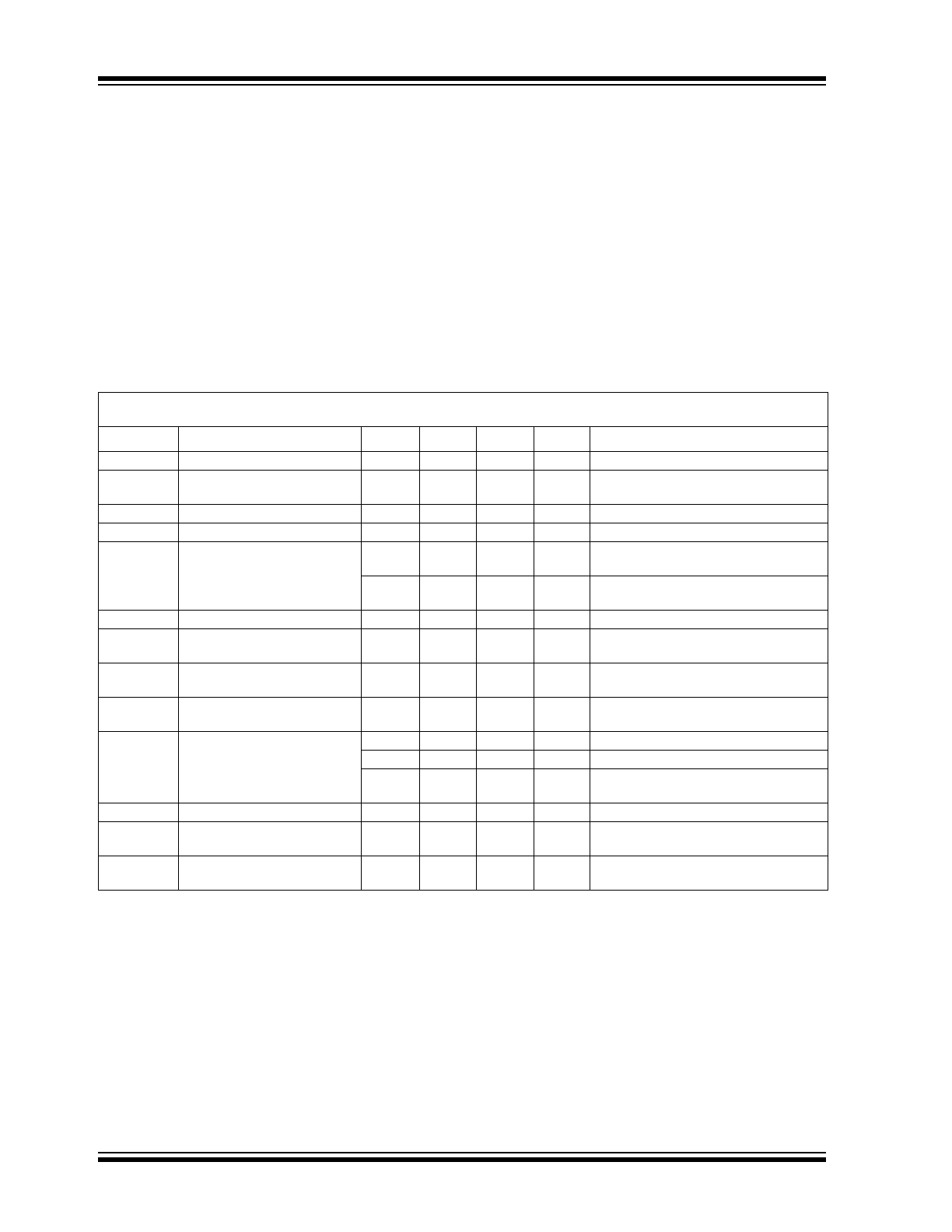
TC1266 ELECTRICAL SPECIFICATIONS
Electrical Characteristics: T
A
= +25°C, V
IN
= 5V, V
AUX
= 3.3V, I
OUT
= 0.1mA, C
OUT
= 4.7
F, unless otherwise noted. Boldface
type specifications apply over full operating temperature range.
Symbol
Parameter
Min.
Typ.
Max.
Units
Test Conditions
V
IN
Supply Voltage
4.3
5.0
5.5
V
V
AUX
= 0V
I
GND
Ground Current
—
—
230
260
450
500
A
V
AUX
= 0V (Note 6)
V
AUX
= 3.3V (Note 6)
I
VIN
Reverse Leakage from V
AUX
—
-0.1
-1.0
A
V
AUX
= 3.6V, V
IN
= 0V, I
OUT
= 0mA
V
AUX
Supply Voltage
3.0
3.3
3.6
V
I
Q(AUX)
Quiescent Current
—
—
50
—
70
100
A
V
IN
= 0V, I
OUT
= 0mA
—
—
60
—
80
120
A
V
IN
= 5V, I
OUT
= 0mA
I
VAUX
Reverse Leakage from V
IN
—
-0.1
-1.0
A
V
IN
= 5,5V, V
AUX
= 0V, I
OUT
= 0mA
V
TH(LO)
5V Detector
Low Threshold Voltage
—
3.75
3.90
—
—
4.05
V
V
IN
Falling (Notes 2, 3)
V
HYST
5V Detector
Hysteresis Voltage
—
200
260
—
—
300
mV
(Notes 2, 3)
V
TH(HI)
5V Detector
High Threshold Voltage
—
4.0
4.15
—
—
4.30
V
V
IN
Rising (Notes 2, 3)
V
OUT
LDO Output Voltage
—
3.300
—
V
I
OUT
= 20mA
3.234
—
3.366
4.3V
V
IN
5.5V, 0mA I
OUT
200mA
3.000
—
—
3.75V
V
IN
V,
0mA
I
OUT
200mA (Note 4)
I
OUT
Output Current
200
—
—
mA
REG
(LINE)
Line Regulation
—
-0.5
0.05
—
—
0.5
%
V
IN
= 4.3V to 5.5V
REG
(LOAD)
Load Regulation
—
-0.5
0.05
—
—
0.5
%
I
OUT
= 0.1mA to 200mA
Note
1:
Ensured by design.
2:
See 5V Detect Thresholds, Figure 4-1.
3:
Recommended source impedance for 5V supply:
0.25. This will ensure that I
OUT
x R
SOURCE
< V
HYST
, thus avoiding D
R
toggling during
5V detect threshold transitions.
4:
In Application Circuit, Figure 3-1.
5:
See Timing Diagram, Figure 4-2.
6:
Ground Current is independent of I
LOAD
.
2001-2014 Microchip Technology Inc.
DS20001377D-page 3
TC1266
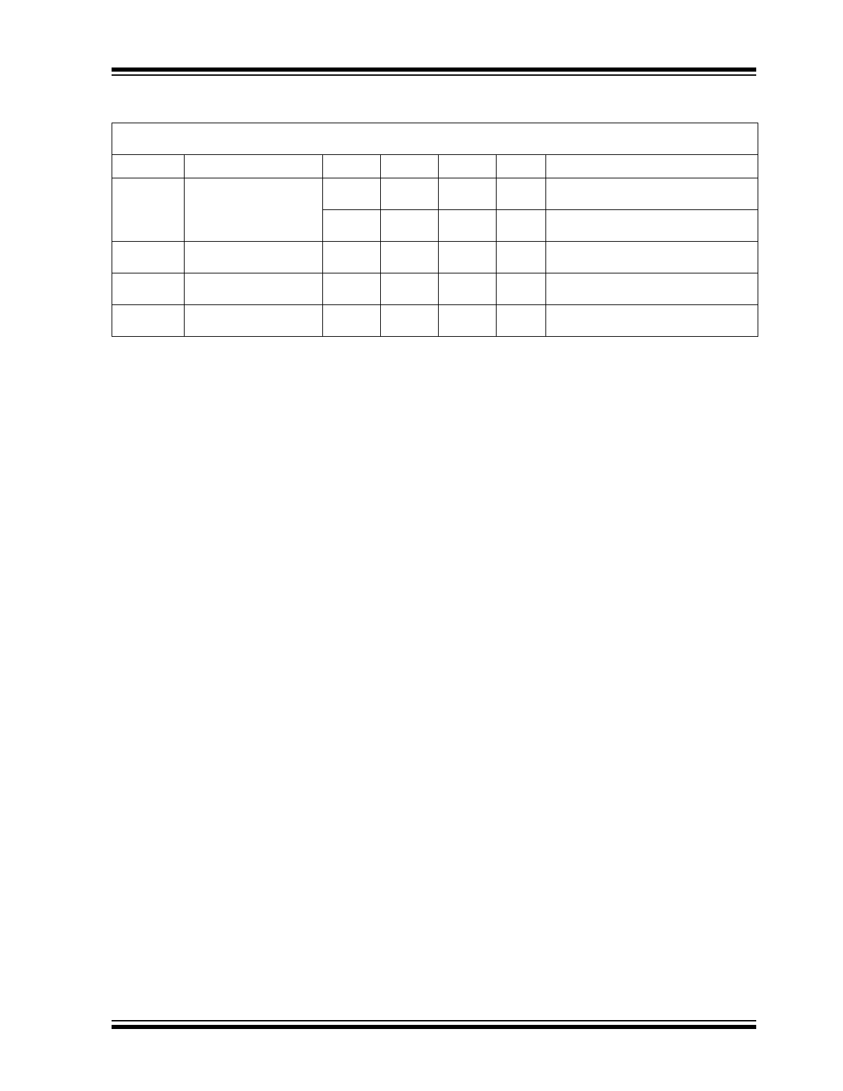
TC1266 ELECTRICAL SPECIFICATIONS
(CONTINUED)
Electrical Characteristics: T
A
= +25°C, V
IN
= 5V, V
AUX
= 3.3V, I
OUT
= 0.1mA, C
OUT
= 4.7
F, unless otherwise noted. Boldface
type specifications apply over full operating temperature range.
Symbol
Parameter
Min.
Typ.
Max.
Units
Test Conditions
V
DR
Drive Voltage
V
IN
- 0.2
V
IN
- 0.3
V
IN
- 0.1
—
—
—
V
4.3V
V
IN
5.5V, I
DR
= 200
A
—
—
35
—
150
200
mV
V
IN
< V
TH(LO)
, I
DR
= 200
A
I
DR(PK)
Peak Drive Current
7
6
—
—
—
—
mA
Sinking: V
IN
= 3.75V, V
DR
= 1V;
Sourcing: V
IN
= 4.3V, V
IN
– V
DR
= 2V
t
DH
Drive High Delay
(Notes 1, 5)
—
—
4
—
—
8
sec
C
DR
= 1.2nF, V
IN
ramping up,
measured from V
IN
= V
TH(HI)
to V
DR
= 2V
t
DL
Drive Low Delay
(Notes 1, 5)
—
—
0.6
—
1.5
3.0
sec
C
DR
= 1.2nF, V
IN
ramping down,
measured from V
IN
= V
TH(LO)
to V
DR
= 2V
Note
1:
Ensured by design.
2:
See 5V Detect Thresholds, Figure 4-1.
3:
Recommended source impedance for 5V supply:
0.25. This will ensure that I
OUT
x R
SOURCE
< V
HYST
, thus avoiding D
R
toggling during
5V detect threshold transitions.
4:
In Application Circuit, Figure 3-1.
5:
See Timing Diagram, Figure 4-2.
6:
Ground Current is independent of I
LOAD
.
TC1266
DS20001377D-page 4
2001-2014 Microchip Technology Inc.
2.0
PIN DESCRIPTIONS
The descriptions of the pins are listed in Table 2-1.
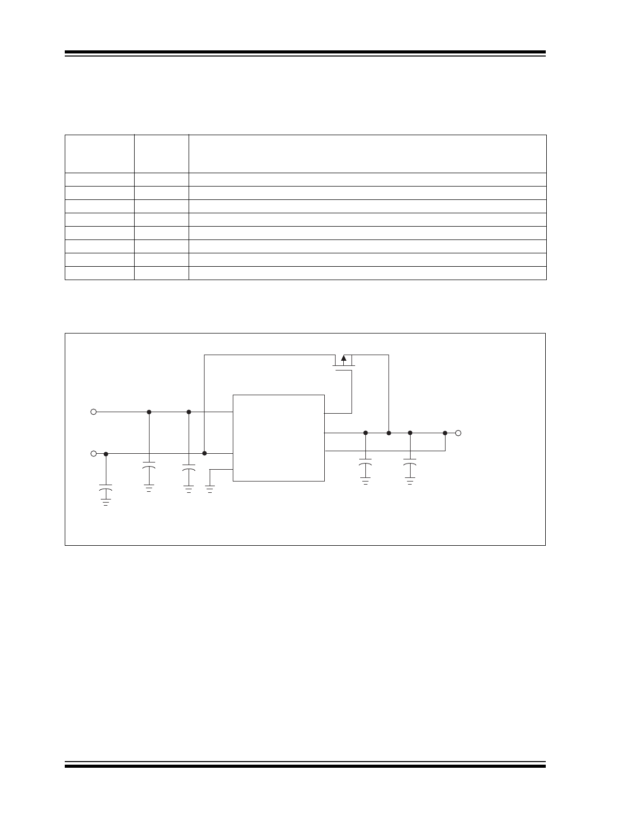
TABLE 2-1:
PIN FUNCTION TABLE
3.0
DETAILED DESCRIPTION
FIGURE 3-1:
APPLICATION CIRCUIT
Pin No.
(8-Pin SOIC)
(8-Pin MSOP)
Symbol
Description
1
V
IN
Main input supply for the TC1266, nominally 5V.
2
NC
Not connected.
3
V
AUX
Auxiliary input supply, nominally 3.3V.
4
GND
Logic and power ground.
5
NC
Not connected.
6
SENSE
Sense pin for V
OUT
. Connect to V
OUT
at the load to minimize voltage drop across PCB traces.
7
V
OUT
LDO 3.3V output.
8
D
R
Driver output for external P-channel MOSFET pass element.
V
IN
NC
V
AUX
GND
NC
SENSE
V
OUT
D
R
U1
TC1266
1
2
3
4
5
6
7
8
NOTE: External switch (Q1): use Motorola MGSF1P02ELT1 or equivalent
(PMOS, typical Gate Threshold Voltage = 1V, typical R
DS(ON)
= 0.4
Ω at VGS = 2.5V)
5V
3.3V
Q1
C1
0.1
μF
C2
4.7
μF
C3
0.1
μF
C4
4.7
μF
C5
0.1
μF
3.3V

2001-2014 Microchip Technology Inc.
DS20001377D-page 5
TC1266
4.0
THERMAL CONSIDERATIONS
4.1
Thermal Shutdown
Integrated thermal protection circuitry shuts the
regulator off when die temperature exceeds 160°C.
The regulator remains off until the die temperature
drops to approximately 150°C.
4.2
Power Dissipation
The amount of power the regulator dissipates is
primarily a function of input and output voltage, and
output current. The following equation is used to
calculate worst case actual power dissipation:
EQUATION 4-1:
The maximum allowable power dissipation
(Equation 4-2) is a function of the maximum ambient
temperature (T
A
MAX
), the maximum allowable die
temperature (T
J
MAX
) and the thermal resistance from
junction-to-air (
JA
).
EQUATION 4-2:
Equation 4-1 can be used in conjunction with
Equation 4-2 to ensure regulator thermal operation is
within limits. For example:
Given:
V
IN
MAX
= 5V ± 5%
V
OUT
MIN
= 3.217V
I
LOAD
MAX
= 200mA
T
J
MAX
= 125°C
T
A
MAX
= 70°C
JA
= 130°C/W (SOIC)
Find: 1. Actual power dissipation
2. Maximum allowable dissipation
Actual power dissipation:
P
D
(V
IN
MAX
– V
OUT
MIN
)I
LOAD
MAX
= (5.25V - 3.217V) 200mA
= 407mW
Maximum allowable power dissipation:
In this example, the TC1266 dissipates a maximum of
407mW; below the allowable limit of 423mW.
Where:
P
D
(V
IN
MAX
– V
OUT
MIN
)I
LOAD
MAX
P
D
V
IN
MAX
V
OUT
MIN
I
LOAD
MAX
= Worst case actual power dissipation
= Minimum regulator output voltage
= Maximum output (load) current
= Maximum voltage on V
IN
P
D
MAX
= (T
J
MAX
– T
A
MAX
)
JA
Where all terms are previously defined.
P
D
MAX
= (T
J
MAX
– T
A
MAX
)
JA
= (125 – 70)
130
= 423mW
TC1266
DS20001377D-page 6
2001-2014 Microchip Technology Inc.
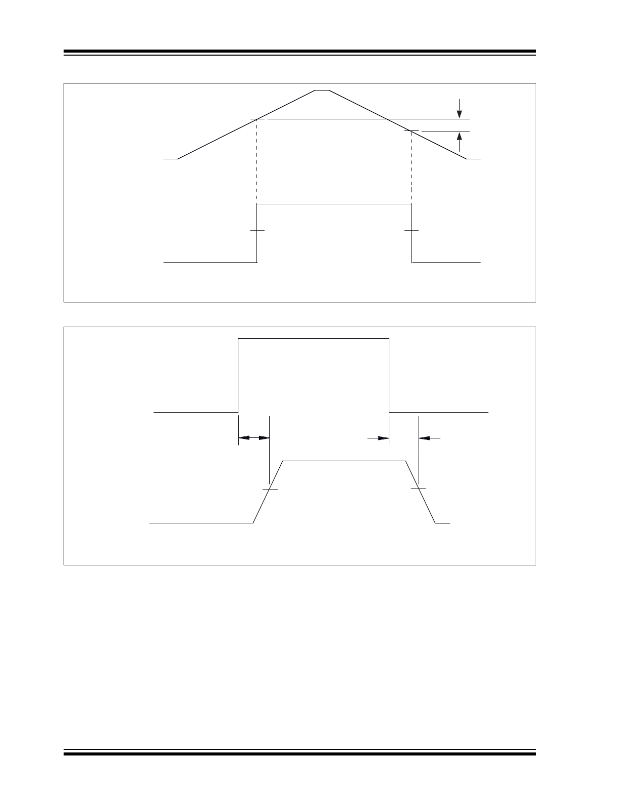
FIGURE 4-1:
5V DETECT THRESHOLD
FIGURE 4-2:
TIMING DIAGRAM
NOTE: V
IN
rise and fall times (10% to 90%) to be
≥ 100μsec.
D
R
V
IN
3.65V
2.0V
4.4V
2.0V
V
TH(HI)
V
HYST
V
TH(LO)
D
R
V
IN
2.0V
4.4V
2.0V
NOTE: V
IN
rise and fall times (10% to 90%) to be
≤ 0.1μsec.
3.65V
t
DH
t
DL
2001-2014 Microchip Technology Inc.
DS20001377D-page 7
TC1266
5.0
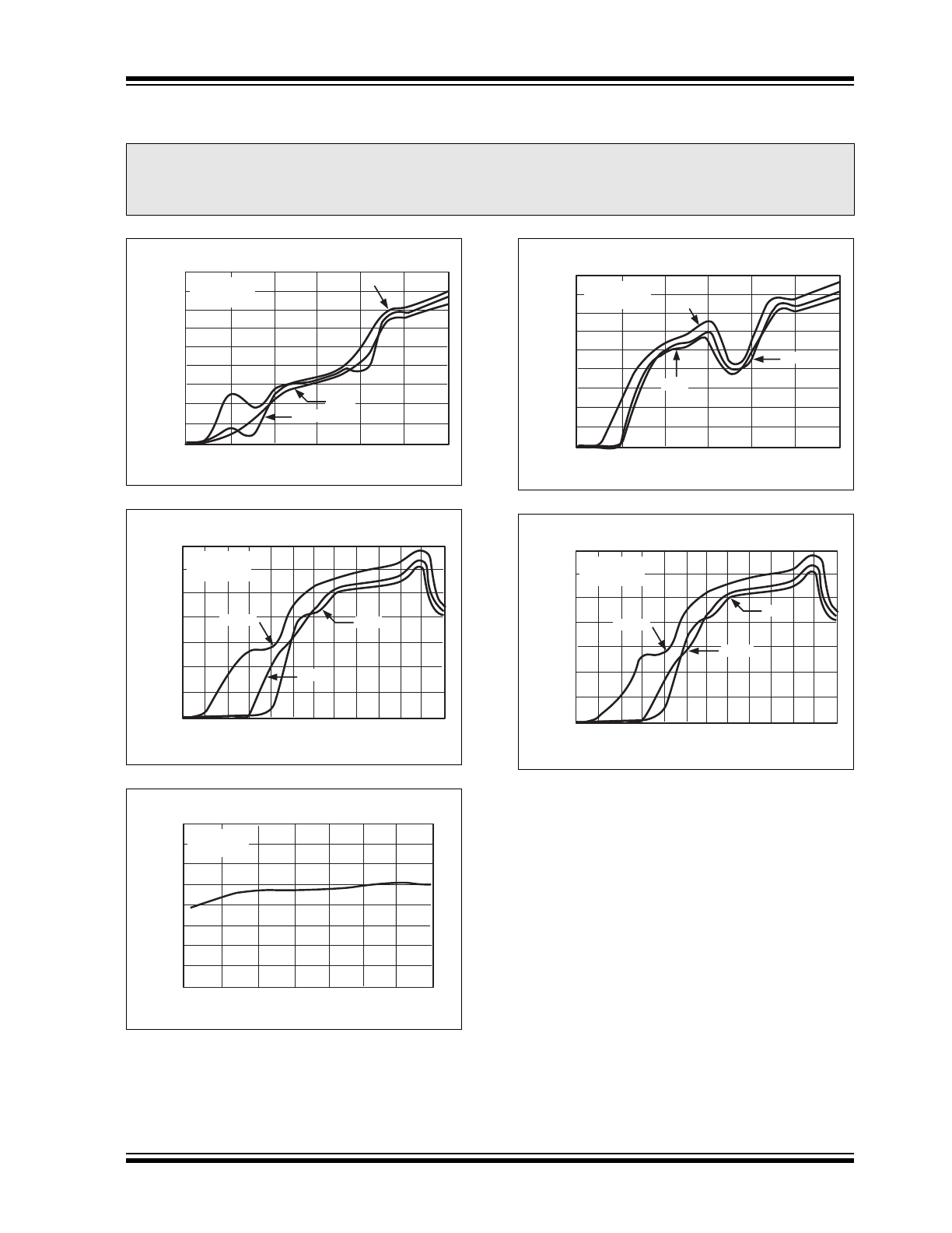
TYPICAL CHARACTERISTICS
Note:
The graphs and tables provided following this note are a statistical summary based on a limited number of
samples and are provided for informational purposes only. The performance characteristics listed herein are
not tested or guaranteed. In some graphs or tables, the data presented may be outside the specified
operating range (e.g., outside specified power supply range) and therefore outside the warranted range.
0.45
0.40
0.35
0.30
0.25
0.20
0.15
0.10
0.05
0.00
I
Q
vs. V
IN
vs. Junction Temperature
0
1
2
3
4
5
6
V
IN
(V)
I
Q
(mA)
I
O
= 0.1mA
V
AUX
= 0V
+125
°C
+25
°C
-5
°C
0.35
0.30
0.25
0.20
0.15
0.10
0.05
0.00
I
Q
(Aux) vs. V
AUX
vs. Junction Temperature
0
0.3 0.6 0.9 1.2 1.5 1.8 2.1 2.4 2.7
3
3.3 3.6
V
AUX
(V)
I
Q
(Aux) (mA)
I
O
= 0mA
V
AUX
= 0V
+125
°C
+25
°C
-5
°C
3.34
3.33
3.32
3.31
3.30
3.29
3.28
3.27
3.26
LDO Output Voltage vs. Junction Temperature
-50
-25
0
25
50
75
100
125
V
OUT
(V)
I
O
= 200mA
V
IN
= 5V
JUNCTION TEMPERATURE
°C
I
Q
vs. V
IN
vs. Junction Temperature
0
1
2
3
4
5
6
V
IN
(V)
0.45
0.40
0.35
0.30
0.25
0.20
0.15
0.10
0.05
0.00
I
Q
(mA)
I
O
= 0.1mA
V
AUX
= 3.3V
+125
°C
+25
°C
-5
°C
0.35
0.30
0.25
0.20
0.15
0.10
0.05
0.00
I
Q
(Aux) vs. V
AUX
vs. Junction Temperature
0
0.3 0.6 0.9 1.2 1.5 1.8 2.1 2.4 2.7
3
3.3 3.6
V
AUX
(V)
I
Q
(Aux) (mA)
I
O
= 0mA
V
AUX
= 5V
+125
°
C
+25
°
C
-5
°
C
TC1266
DS20001377D-page 8
2001-2014 Microchip Technology Inc.
5.0
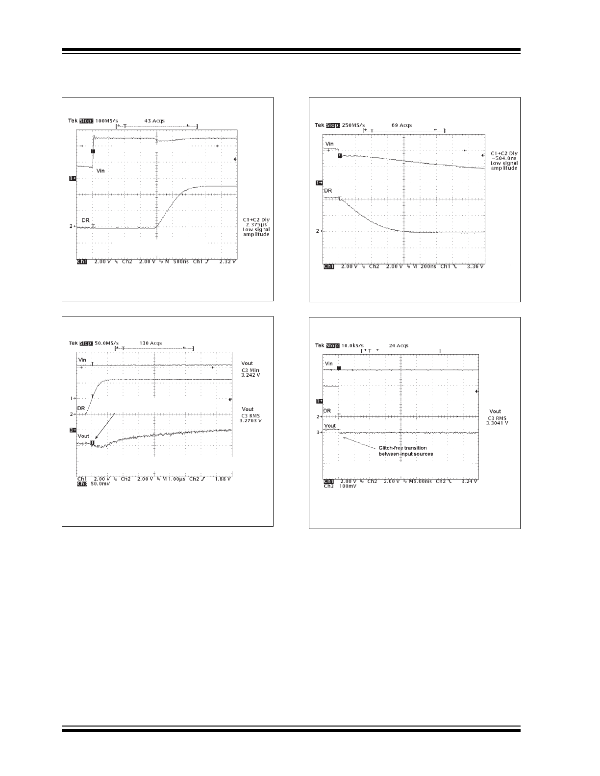
TYPICAL CHARACTERISTICS (CONTINUED)
Trace 1: V
IN
stepping for 0.8V to 5V
Trace 2: D
R
going high at V
TH(HI)
TDH = < 4
PS
Drive High Delay
4
See application circuit on Page 5
I
LOAD
= 200mA
V
IN
steps from 0.8V to 5V
Trace 1: V
IN
– 3A charging a 1500
µF capacitor
Trace 2: D
R
going high at V
TH(HI)
Trace 3: V
OUT
, offset 3.3V. V
OUT(min)
= 3.24V
I
LOAD
= 200
µA
V
O
(min) with V
IN
Rising
Notice no voltage spikes during transition
from V
AUX
to LDO output
V
OUT
voltage difference is I
OUT
x R
DS(ON)
and variations
between V
AUX
supply and LDO output voltage
Trace 1: VIN stepping for 5.5V to 0V
Trace 2: DR going low
TDL = < 600nS
Drive Low Delay
Trace 1: V
IN
– discharging a 1500
µF capacitor
Trace 2: D
R
going low at V
TH(LO)
Trace 3: V
OUT
, offset 3.3V. V
OUT(min)
= 3.14V
I
LOAD
= 200
µA
V
O
(min) with V
IN
Falling
V
OUT
voltage difference is I
OUT
x R
DS(ON)
+ voltage
difference from LDO to V
AUX
supply
2001-2014 Microchip Technology Inc.
DS20001377D-page 9
TC1266
5.0
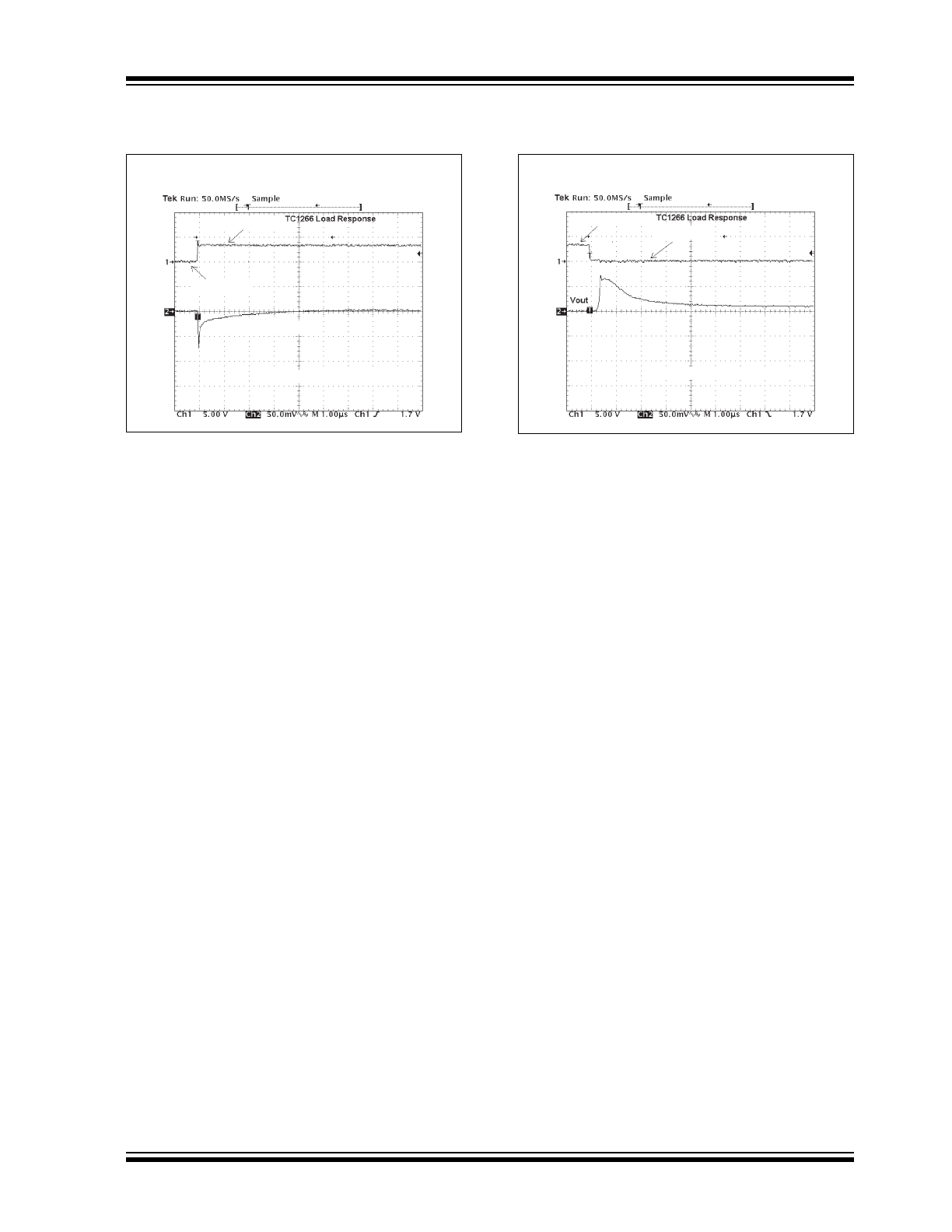
TYPICAL CHARACTERISTICS (CONTINUED)
Load Response Rising Edge
See application circuit on Page 5
V
OUT
AC 60mV/div
I
LOAD
= 3mA
I
LOAD
= 200mA
Load Response Falling Edge
4
See application circuit on Page 5
I
LOAD
= 3mA
I
LOAD
= 200mA
TC1266
DS20001377D-page 10
2001-2014 Microchip Technology Inc.
6.0
PACKAGING INFORMATION
6.1
Package Marking Information
Package marking data not available at this time.
6.2
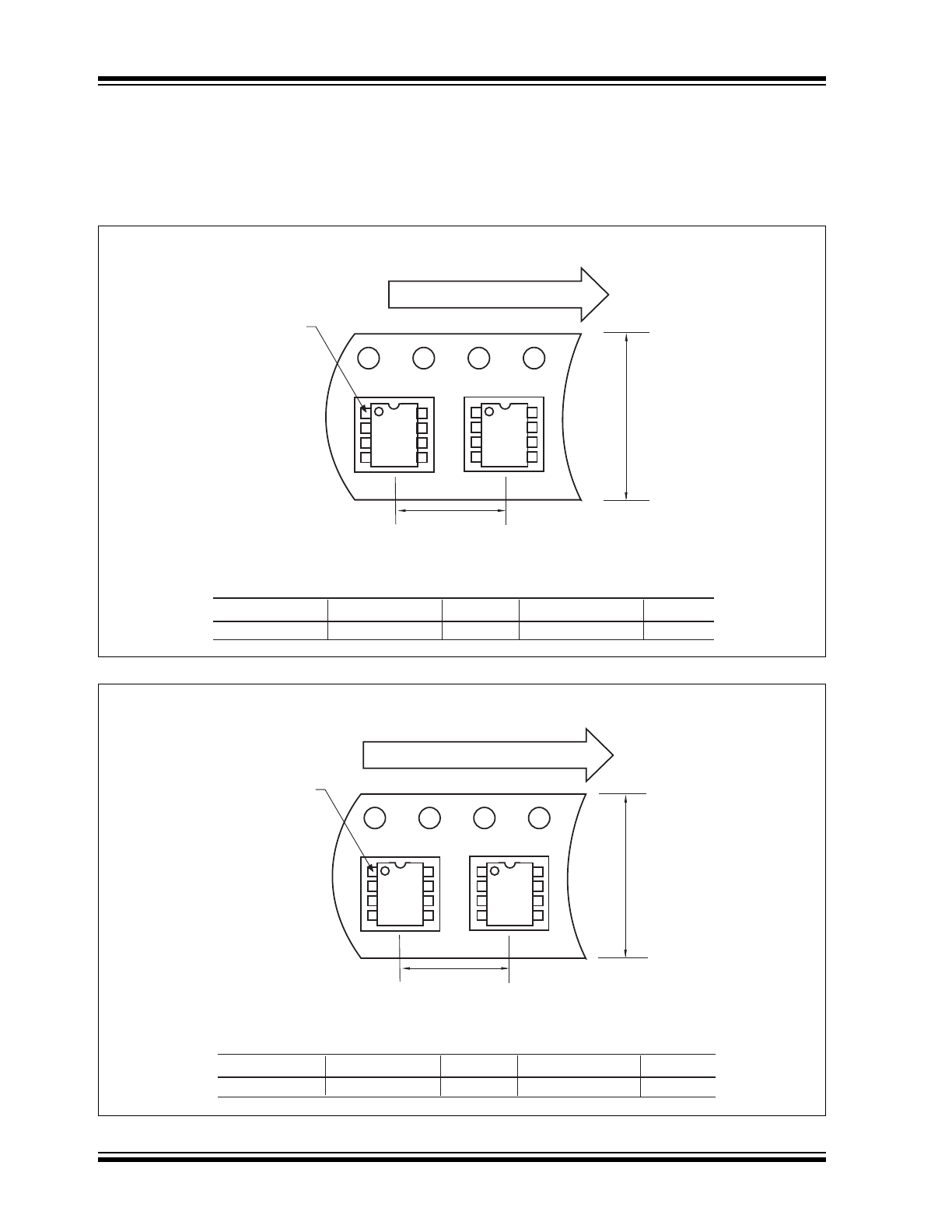
Taping Form
Component Taping Orientation for 8-Pin MSOP Devices
Package
Carrier Width (W)
Pitch (P)
Part Per Full Reel
Reel Size
8-Pin MSOP
12 mm
8 mm
2500
13 in
Carrier Tape, Number of Components Per Reel and Reel Size
PIN 1
User Direction of Feed
Standard Reel Component Orientation
for TR Suffix Device
W
P
Component Taping Orientation for 8-Pin SOIC (Narrow) Devices
Package
Carrier Width (W)
Pitch (P)
Part Per Full Reel
Reel Size
8-Pin SOIC (N)
12 mm
8 mm
2500
13 in
Carrier Tape, Number of Components Per Reel and Reel Size
Standard Reel Component Orientation
for TR Suffix Device
PIN 1
User Direction of Feed
P
W