
2002-2014 Microchip Technology Inc.
DS20001370E-page 1
TC1232
Features:
• Precision Voltage Monitor:
- Adjustable +4.5V or +4.75V
• Reset Pulse Width – 250 ms minimum
• No External Components
• Adjustable Watchdog Timer:
- 150 ms, 600 ms or 1.2s
• Operating Voltage 4.0V to 5.5V
• Debounced Manual Reset Input for External
Override
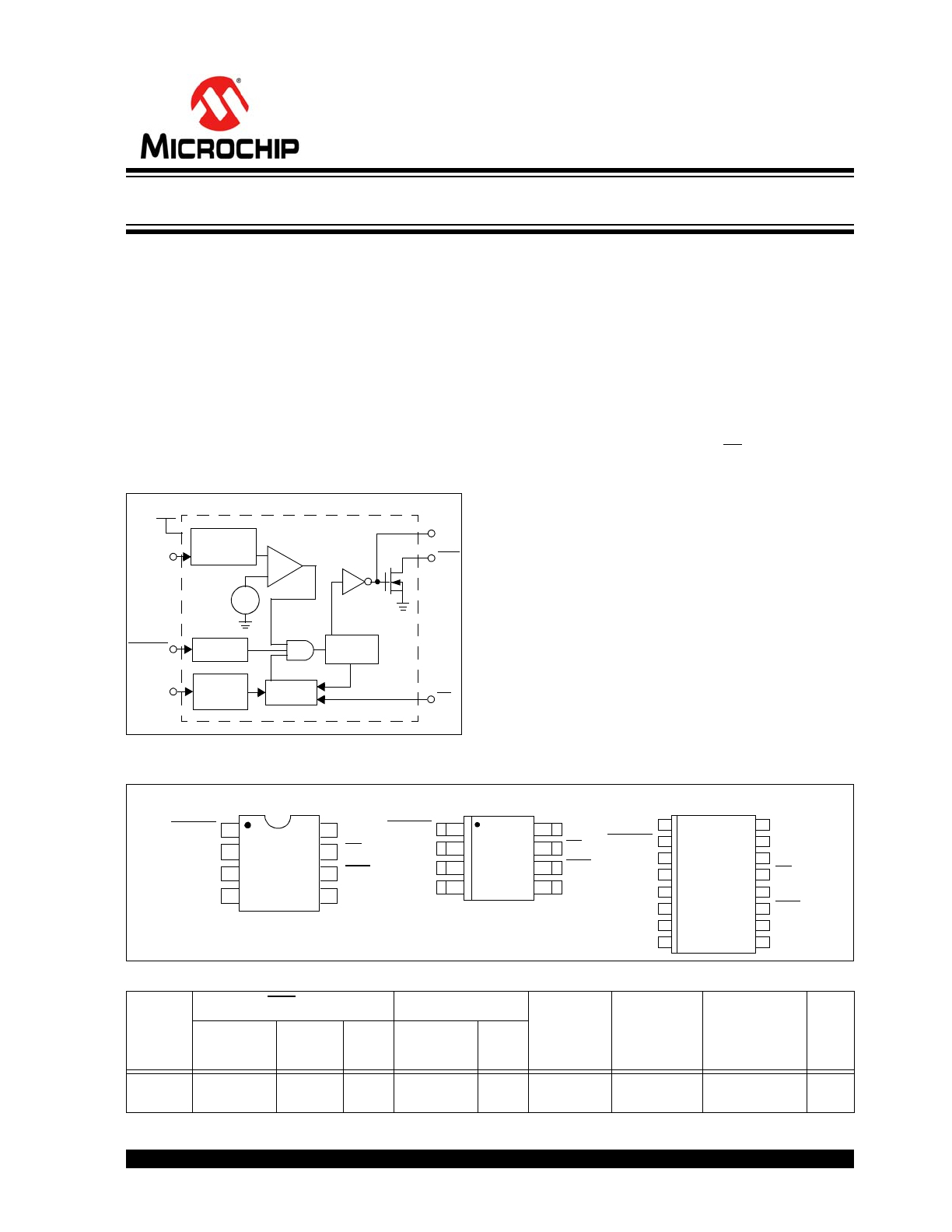
Block Diagram
General Description:
The TC1232 is a fully-integrated processor supervisor
that provides three important functions to safeguard
processor sanity: precision power on/off Reset control,
Watchdog Timer and external Reset override.
On power-up, the TC1232 holds the processor in the
Reset state for a minimum of 250 ms after V
CC
is within
tolerance to ensure a stable system start-up.
Microprocessor sanity is monitored by the on-board
watchdog circuit. The microprocessor must provide a
periodic low-going signal on the ST input. Should the
processor fail to supply this signal within the selected
time-out period (150 ms, 600 ms or 1200 ms), an out-
of-control processor is indicated and the TC1232
issues a processor Reset as a result.
The outputs of the TC1232 are immediately driven
active when the PB input is brought low by an external
push button switch or other electronic signal. When
connected to a push button switch, the TC1232
provides contact debounce.
The TC1232 is packaged in a space-saving 8-Pin PDIP
or SOIC package, a 16-Pin SOIC (wide) package and
requires no external components.
Package Types
Device Features
+
–
V
REF
+
+
–
RST
RST
Tolerance
Select
(5% or 10%)
TOL
V
CC
Debounce
Watchdog
Timebase
Select
PB RST
TD
Watchdog
Timer
ST
Reset
Generator
Device
RST pin
RST pin
Trip Points
(Max)
Minimum
Reset
Active Time
(ms)
WDI Input
Typical
Timeouts (ms)
MR
Input
Type
Pull-up
Resistor
Active
Level
Type
Active
Level
TC1232
Open-drain
External
Low
Push-pull
High
4.75V
or 4.5V
250
150, 600 or
1200
Yes
13
12
11
10
9
15
14
1
8
2
7
3
6
4
5
TC1232
RST
RST
GND
TOL
TD
PB RST
RST
ST
V
CC
RST
ST
1
8
2
7
3
6
4
5
RST
GND
TOL
TD
PB RST
RST
ST
V
CC
PB RST
VCC
1
2
3
4
5
6
7
8
16
NC
TD
NC
NC
TOL
GND
NC
NC
NC
TC1232
NC
NC
16-Pin SOIC (Wide)
8-Pin PDIP
8-Pin SOIC
TC1232
1
8
3
6
4
5
TC1232
Microprocessor Monitor
TC1232
DS20001370E-page 2
2002-2014 Microchip Technology Inc.
1.0
ELECTRICAL
CHARACTERISTICS
Absolute Maximum Ratings†
Voltage on Any Pin (With Respect to GND)
...................................................... -0.3V to +5.8V
Operating Temperature Range:
C-Version ........................................ 0°C to +70°C
E-Version...................................... -40°C to +85°C
Storage Temperature Range: ............-65°C to +150°C
† Stresses above those listed under "Absolute Maximum
Ratings" may cause permanent damage to the device. These
are stress ratings only and functional operation of the device
at these or any other conditions above those indicated in the
operation sections of the specifications is not implied.
Exposure to Absolute Maximum Rating conditions for
extended periods may affect device reliability.
DC CHARACTERISTICS
Electrical Specifications: Unless otherwise noted, T
A
= T
MIN
to T
MAX
; V
CC
= +4.0V to 5.5V.
Parameters
Sym.
Min.
Typ.
Max.
Units
Conditions
Supply Voltage
V
CC
4.0
5.0
5.5
V
ST and PB RST Input High Level
V
IH
2.0
—
V
CC
+0.3
V
Note 1
ST and PB RST Input Low Level
V
IL
-0.3
—
+0.8
V
Input Leakage ST, TOL
I
L
-1.0
—
+1.0
µA
Output Current RST
I
OH
-1.0
-12
—
mA
V
OH
= 2.4V
Current RST, RST
I
OL
2.0
10
—
mA
V
OL
= 0.4V
Operating Current
I
CC
—
50
200
µA
Note 2
V
CC
5% Trip Point
V
CCTP
4.50
4.62
4.74
V
TOL = GND (
Note 3
)
V
CC
10% Trip Point
V
CCTP
4.25
4.37
4.49
V
TOL = V
CC
(
Note 3
)
Capacitance Electrical Characteristics: Unless otherwise noted, T
A
= +25°C. (
Note 4
)
Input Capacitance ST, TOL
C
IN
—
—
5
pF
Output Capacitance RST, RST
C
OUT
—
—
7
pF
Note 1:
PB RST is internally pulled up to V
CC
with an internal impedance of typically 40 k
.
2:
Measured with outputs open.
3:
All voltages referenced to GND.
4:
Ensured by design.
2002-2014 Microchip Technology Inc.
DS20001370E-page 3
TC1232
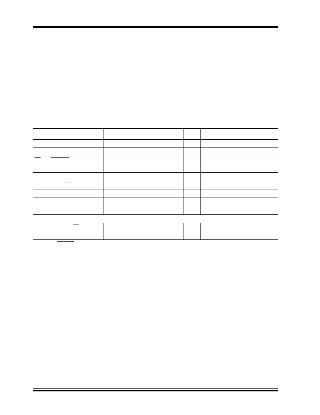
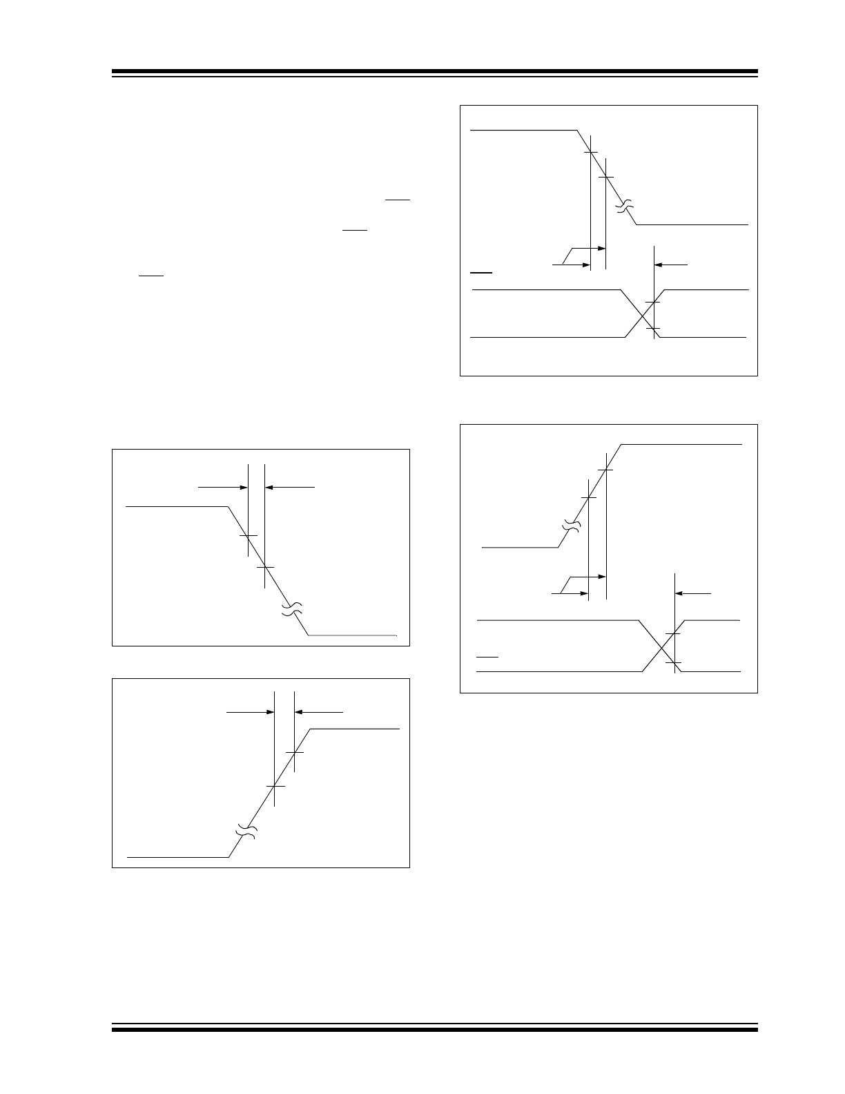
FIGURE 1-1:
Rise Time, Fall Time and Reset Detected to Reset Active Timing Waveforms.
AC CHARACTERISTICS
Electrical Specifications: Unless otherwise noted, T
A
= T
MIN
to T
MAX
; V
CC
= +4.0V to 5.5V.
Parameters
Sym.
Min.
Typ.
Max.
Units
Conditions
V
CC
Fall Time
t
F
10
—
—
µs
Note 1
V
CC
Rise Time
t
R
0
—
—
µs
Note 1
V
CC
Trip Point Detected
to RST High and RST Low
t
RPD
—
—
100
ns
V
CC
falling
V
CC
Trip Point Detected
to RST High and RST Open
t
RPU
250
610
1000
ms
V
CC
rising (
Note 2
)
Note 1:
Ensured by design.
2:
t
R
= 5 µs.
+4.75V
t
F
V
CC
+4.25V
t
R
V
CC
+4.25V
+4.75V
V
CC
= 5V
+4.5V (5% Trip Point)
+4.25V (10% Trip Point)
RST
RST
V
OL
V
OH
t
RPD
V
CC
4.6V (5% Trip Point)
4.5V(10% Trip Point)
RST
RST
V
OL
V
OH
t
RPU
Determined by
external Pull-up
resistor
Determined by
external Pull-up
resistor
TC1232
DS20001370E-page 4
2002-2014 Microchip Technology Inc.
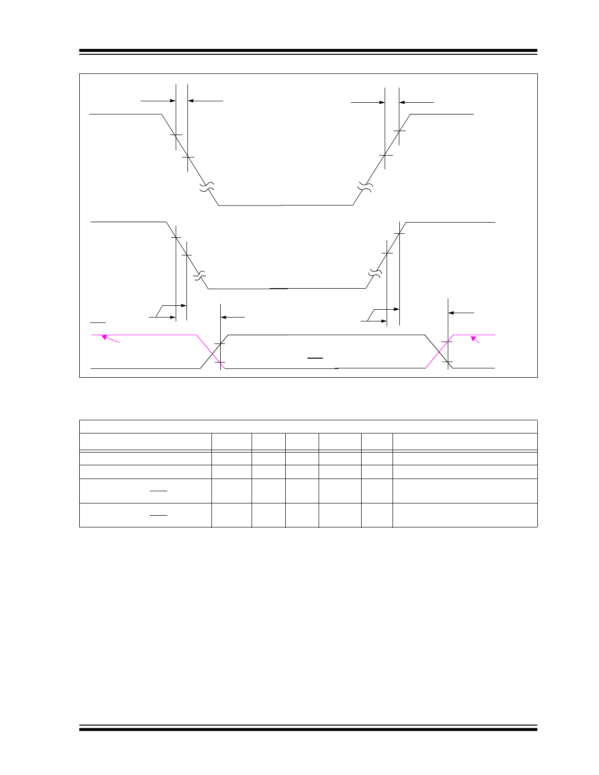
FIGURE 1-2:
Push Button Reset and Watchdog Timer Reset Timing Waveforms.
AC CHARACTERISTICS (CONTINUED)
Electrical Specifications: Unless otherwise noted, T
A
= T
MIN
to T
MAX
; V
CC
= +4.0V to 5.5V.
Parameters
Sym.
Min.
Typ.
Max.
Units
Conditions
PB RST Pulse Width
t
PB
20
—
—
ms
Note 1
PB RST Falling Edge Low to
Reset Active
t
PBD
1
4
20
ms
PB RST Rising Edge High to
Reset Inactive
t
RST
250
610
1000
ms
ST Pulse Width
t
ST
20
—
—
ns
ST Time-out Period
t
TD
62.5
150
250
ms
TD Pin = 0V
250
600
1000
ms
TD Pin = Open
500
1200
2000
ms
TD Pin = V
CC
Note 1:
PB RST must be held low for a minimum of 20 ms to ensure a Reset.
RST
V
IL
t
PB
RST
t
PBD
V
IH
t
RST
PB RST
The debounced PB RST input ignores input pulses less
than 1 ms and is designed to recognize pulses of
20 ms or greater.
t
ST
ST
t
TD
RST (when t
TD
t
TD
(min))
“H”
RST
(when t
TD
(min)
t
TD
t
TD
(max))
(when t
TD
t
TD
(max))
RST
RST (when t
TD
t
TD
(min))
“L”
RST
(when t
TD
(min)
t
TD
t
TD
(max))
(when t
TD
t
TD
(max))
RST

2002-2014 Microchip Technology Inc.
DS20001370E-page 5
TC1232
2.0
TYPICAL PERFORMANCE CURVES
Performance Graphs are not available.
TC1232
DS20001370E-page 6
2002-2014 Microchip Technology Inc.
3.0
PIN DESCRIPTIONS
The descriptions of the pins are listed in
Table 3-1
.
TABLE 3-1:
PIN FUNCTION TABLES
Pin No.
Symbol
Pin
Type
Buffer/
Driver
Type
Function
8-pin
PDIP,
SOIC
16-pin
SOIC
1
2
PB RST
I
ST
Push Button Reset Input.
Input for a Manual Reset Switch. This input debounces (ignores) pulses
less than 1 ms in duration and is ensured to recognize inputs of 20 ms or
greater.
L = Manual Reset Switch is Active, Force RST/RST pins Active
H = Manual Reset Switch is Inactive. State of RST/RST pins determined by
other system conditions.
2
4
TD
I
ST
Time Delay Input.
The voltage level on this input determines the Watchdog Timer Time-out
period.
TD = 0V
t
TD
= 150 ms
TD = Open
t
TD
= 600 ms
TD = V
CC
t
TD
= 1.2s
3
6
TOL
I
ST
Tolerance Input.
TOL = GND, Max Voltage Trip Point (V
CCTP
) = 4.75V (5% tolerance)
TOL = V
CC
, Max Voltage Trip Point (V
CCTP
) = 4.5V (10% tolerance)
4
8
GND
—
P
The ground reference for the device.
5
9
RST
O
Push
Pull
Reset Output (Active-High)
Goes active (High) if one of these conditions occurs:
1.
If V
CC
falls below the selected Reset voltage threshold.
2.
If PB RST pin is forced low.
3.
If ST pin is not strobed within the minimum selected time-out period.
(see TD pin)
4.
During power-up.
6
11
RST
O
Open
Drain
Reset Output (Active-Low)
Goes active (Low) if one of these conditions occurs:
1.
If V
CC
falls below the selected Reset voltage threshold.
2.
If PB RST pin is forced low.
3.
If ST pin is not strobed within the minimum selected time-out period.
(see TD pin)
4.
During power-up.
7
13
ST
I
ST
Strobe Input
Input for Watchdog Timer. WDT period determined by state of TD pin
Falling Edge
Resets Watchdog Timer counter (no time-out)
8
15
V
CC
—
P
The positive supply (+5V) for the device.
—
1,3,5,
7,10,1
2,16
NC
—
—
No internal connection.
2002-2014 Microchip Technology Inc.
DS20001370E-page 7
TC1232
4.0
OPERATIONAL DESCRIPTION
4.1
Power Monitor
The TC1232 provides the function of warning the
processor of a power failure. When V
CC
is detected as
being below the voltage levels defined by the TOL pin,
the TC1232’s comparator outputs the RST and RST
signals to a logic level that warns the system of an out-
of-tolerance power supply. The RST and RST signals
switch at a threshold value of 4.5V if TOL is tied to V
CC
,
and at a value of 4.75V if TOL is grounded. The RST
and RST signals are held active for a minimum of
250 ms to ensure that the power supply voltage has
been stabilized.
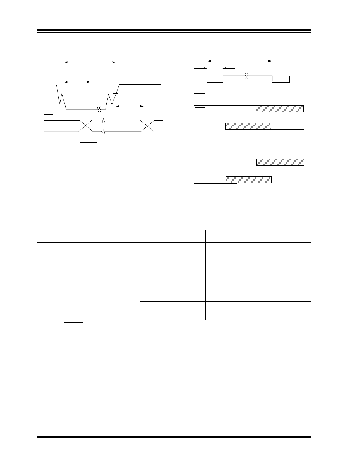
Figure 4-1
shows the V
CC
fall time.
Figure 4-2
shows the V
CC
rise time.
Figure 4-3
shows the time from when the voltage trip
point is detected to the Reset output pin going active.
Figure 4-4
shows the time from when the voltage trip
point is exited to the Reset output pin going inactive.
FIGURE 4-1:
Power-Down Slew Rate.
FIGURE 4-2:
Power-up Slew Rate.
FIGURE 4-3:
V
CC
Detect Reset Output
Delay (Power-Down).
FIGURE 4-4:
V
CC
Detect Reset Output
Delay (Power-Up).
+4.75V
t
F
V
CC
+4.25V
t
R
V
CC
+4.25V
+4.75V
V
CC
= 5V
+4.5V (5% Trip Point)
+4.25V (10% Trip Point)
RST
RST
V
OL
V
OH
t
RPD
V
CC
SLEW RATE = 1.66 mV/µs (0.5V/300 µs)
V
CC
4.6V (5% Trip Point)
4.5V(10% Trip Point)
RST
RST
V
OL
V
OH
t
RPU
TC1232
DS20001370E-page 8
2002-2014 Microchip Technology Inc.
4.2
Push Button Reset Input
The debounced manual Reset input (PB RST) manu-
ally forces the Reset outputs into their active states.
Figure 4-5
shows a block diagram for using the
TC1232 with a push button switch.
Once PB RST has been low for a time t
PBD
(the push
button delay time), the Reset outputs go active. The
Reset outputs remain in their active states for a
minimum of 250 ms after PB RST rises above V
IH
.
Figure 4-6
shows a waveform for the push button
switch input and the Reset pins output.
A mechanical push button or active logic signal can
drive the PB RST input. The debounced input ignores
input pulses less than 1 ms and recognizes pulses of
20 ms or greater. No external pull-up resistor is
required
because the PB RST input has an internal
pull-up to
V
CC
of
approximately 100 µA.
FIGURE 4-5:
Push Button Reset and
Watchdog Timer.
FIGURE 4-6:
Push Button Reset –
PB RST Input.
V
CC
TOL
PB RST
GND
RST
ST
I/O
Reset
+5V
TC1232
TD
Microprocessor
RST
V
IL
t
PB
RST
t
PBD
V
IH
t
RST
PB RST
The debounced PB RST input ignores input pulses less
than 1 ms and is designed to recognize pulses of
20 ms or greater.
2002-2014 Microchip Technology Inc.
DS20001370E-page 9
TC1232
4.3
Watchdog Timer
When the ST input is not stimulated for a preset time
period, the Watchdog Timer function forces RST and
RST signals to the active state. The preset time period
is determined by the TD inputs to be 150 ms with TD
connected to ground, 600 ms with TD floating or
1200 ms with TD connected to V
CC
(typ.). The
Watchdog Timer starts timing-out from the set time
period as soon as RST and RST are inactive. If a high-
to-low transition occurs on the ST input pin prior to
time-out, the Watchdog Timer is reset and begins to
time-out again. If the Watchdog Timer is allowed to
time-out, the RST and RST signals are driven to the
active state for 250 ms, minimum (
Figure 4-7
).
The software routine that strobes ST is critical. The
code must be in a section of software that is executed
frequently enough so the time between toggles is less
than the Watchdog Time-out period. One common
technique controls the microprocessor I/O line from two
sections of the program. The software might set the I/O
line high while operating in the Foreground mode and
set it low while in the Background or Interrupt modes. If
both modes do not execute correctly, the Watchdog
Timer issues Reset pulses.
t
TD
is the maximum elapsed time between ST high-to-
low transitions (ST is activated by falling edges only),
which will keep the Watchdog Timer from forcing the
Reset outputs active for a time of t
RST
. t
TD
is a function
of the voltage at the TD pin, as tabulated below:
TABLE 4-1:
WATCHDOG TIMER
PERIODS
Figure 4-7
shows a block diagram for using the
TC1232 with a PIC
®
MCU and the Watchdog input.
FIGURE 4-7:
Watchdog Timer.
Figure 4-8
shows the expected Reset output pin wave-
forms depending on the period of the ST pin falling
edge and the state of the TD input pin.
FIGURE 4-8:
Strobe Input.
4.4
Supply Monitor Noise Sensitivity
The TC1232 is optimized for fast response to negative-
going changes in V
DD
. Systems with an inordinate
amount of electrical noise on V
DD
(such as systems
using relays) may require a 0.01 µF or 0.1 µF bypass
capacitor to reduce detection sensitivity. This capacitor
should be installed as close to the TC1232 as possible
to keep the capacitor lead length short.
Condition
t
TD
Min.
Typ.
Max.
TD pin = 0V
62.5 ms
150 ms
250 ms
TD pin = Open
250 ms
600 ms
1000 ms
TD pin = V
CC
500 ms
1200 ms
2000 ms
V
CC
TOL GND
RST
ST
RESET
+5V
TC1232
TD
0.1
10 k
I/O
PIC
®
3-Terminal
Regulator
+5V
µF
MCU
(example:
MCP1700)
t
ST
ST
t
TD
RST (when t
TD
t
TD
(min))
“H”
RST
(when t
TD
(min)
t
TD
t
TD
(max))
(when t
TD
t
TD
(max))
RST
RST (when t
TD
t
TD
(min))
“L”
RST
(when t
TD
(min)
t
TD
t
TD
(max))
(when t
TD
t
TD
(max))
RST
TC1232
DS20001370E-page 10
2002-2014 Microchip Technology Inc.
5.0
PACKAGING INFORMATION
5.1
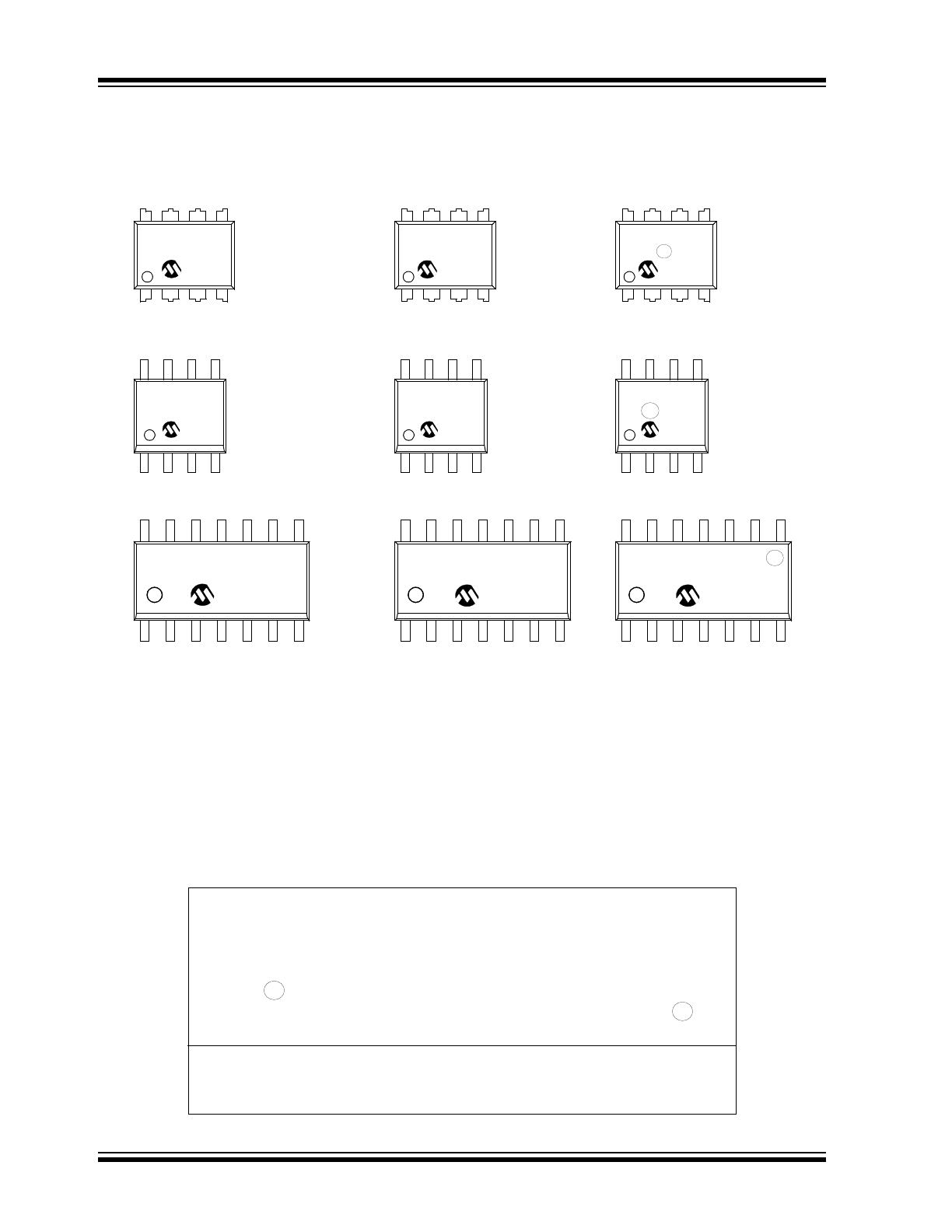
Package Marking Information
XXXXXXXX
XXXXXNNN
YYWW
8-Lead PDIP (300 mil)
Examples:
8-Lead SOIC (150 mil)
Examples:
XXXXXXXX
XXXXYYWW
NNN
TC1232
I/P256
0518
TC1232
COA0518
256
16-Lead SOIC (150 mil)
Examples:
XXXXXXXXXXXXX
YYWWNNN
XXXXXXXXXXXXX
TC1232COE
0518256
XXXXXXXXXX
Legend: XX...X
Customer-specific information
Y
Year code (last digit of calendar year)
YY
Year code (last 2 digits of calendar year)
WW
Week code (week of January 1 is week ‘01’)
NNN
Alphanumeric traceability code
Pb-free JEDEC
®
designator for Matte Tin (Sn)
*
This package is Pb-free. The Pb-free JEDEC designator ( )
can be found on the outer packaging for this package.
Note:
In the event the full Microchip part number cannot be marked on one line, it will
be carried over to the next line, thus limiting the number of available
characters for customer-specific information.
3
e
3
e
TC1232
CPA
^^
256
0518
TC1232E
OA
^^
0518
256
TC1232COE
^^
0518256
XXXXXXXXXX
OR
OR
OR
3
e
3
e
3
e