
2002-2014 Microchip Technology Inc.
DS20001367C-page 1
TC1221/TC1222
Features:
• Charge Pumps in 6-Pin SOT-23A Package
• 96% Voltage Conversion Efficiency
• Voltage Inversion and/or Doubling
• Operates from +1.8V to +5.5V
• Up to 25mA Output Current
• Only Two External Capacitors Required
• Power-Saving Shutdown Mode
• Fully Compatible with 1.8V Logic Systems
Applications:
• LCD Panel Bias
• Cellular Phones
• Pagers
• PDAs, Portable Data Loggers
• Battery-Powered Devices
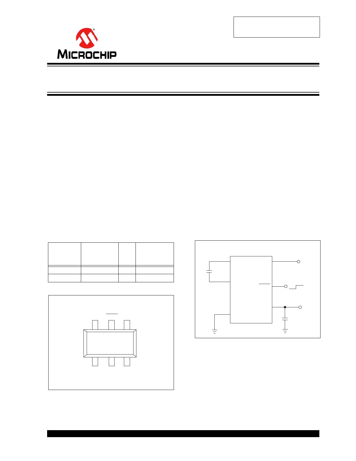
Device Selection Table
Package Type
General Description:
The TC1221/TC1222 are CMOS “charge-pump”
voltage converters in ultra-small 6-Pin SOT-23A
packages. They invert and/or double an input voltage
which can range from +1.8V to +5.5V. Conversion
efficiency is typically 96%. Switching frequency is 125
kHz for the TC1221, 750 kHz for the TC1222. When the
shutdown pin is held at a logic low, the device goes into
a very low power mode of operation, consuming less
than 1
A of supply current.
For standard voltage inverter applications, the device
requires only two external capacitors. With a few
additional components a positive doubler can also be
built. All other circuitry, including control, oscillator,
power MOSFETs are integrated on-chip. Typical supply
currents are 290
A (TC1221) and 1800A (TC1222).
All devices are available in 6-pin SOT-23A surface
mount packages.
Functional Block Diagram
Part
Number
Package
Osc.
Freq.
(kHz)
Operating
Temp.
Range
TC1221ECH 6-Pin SOT-23A
125
-40°C to +85°C
TC1222ECH 6-Pin SOT-23A
750
-40°C to +85°C
C+
C–
TC1221ECH
TC1222ECH
1
2
3
5
4
V
IN
SHDN
GND
6-Pin SOT-23A
NOTE: 6-Pin SOT-23A is equivalent to the EIAJ SC-74
OUT
6
TC1221
TC1222
V
IN
V–
Output
C+
C–
C1
C2
Input
GND
OUT
SHDN
ON
OFF
+
+
Negative Voltage Inverter
High-Frequency Switched Capacitor Voltage Converters
with Shutdown in SOT Packages
Obsolete Device
TC1221/TC1222
DS20001367C-page 2
2002-2014 Microchip Technology Inc.
1.0
ELECTRICAL
CHARACTERISTICS
Absolute Maximum Ratings*
Input Voltage (V
IN
to GND)....................... +6.0V, -0.3V
Output Voltage (OUT to GND).................. -6.0V, +0.3V
Current at OUT Pin..............................................50mA
Short-Circuit Duration – OUT to GND ............Indefinite
Power Dissipation (T
A
70°C)
6-Pin SOT-23A .........................................240mW
Operating Temperature Range............. -40°C to +85°C
Storage Temperature (Unbiased) .......-65°C to +150°C
*Stresses above those listed under "Absolute Maximum
Ratings" may cause permanent damage to the device. These
are stress ratings only and functional operation of the device
at these or any other conditions above those indicated in the
operation sections of the specifications is not implied.
Exposure to Absolute Maximum Rating conditions for
extended periods may affect device reliability.
TC1221/TC1222 ELECTRICAL SPECIFICATIONS
Electrical Characteristics: T
A
= -40°C to +85°C, V
IN
= +5V, C1 = C2 = 1
F, (TC1221), C1 = C2 = 0.22F (TC1222), Typical values
are at T
A
= +25°C.
Symbol
Parameter
Min.
Typ.
Max.
Units
Device
Test Conditions
I
DD
Supply Current
—
—
290
1800
600
2800
A
TC1221
TC1222
I
SHDN
Shutdown Supply Current
—
0.01
1.0
A
SHDN = GND, V
IN
= 5V (Note 2)
V
MIN
Minimum Supply Voltage
1.8
—
—
V
R
LOAD
= 1k
V
MAX
Maximum Supply Voltage
—
—
5.5
V
R
LOAD
= 1k
F
OSC
Oscillator Frequency
81
550
125
750
169
950
kHz
TC1221
TC1222
V
IH
SHDN Input Logic High
1.4
—
V
V
IN
= V
MIN
to V
MAX
V
IL
SHDN Input Logic Low
—
—
0.4
V
V
IN
= V
MIN
to V
MAX
P
EFF
Power Efficiency
—
—
90
70
—
—
%
TC1221
TC1222
R
LOAD
= 1k
V
EFF
Voltage Conversion Efficiency
94
96
—
%
R
LOAD
=
R
OUT
Output Resistance
—
—
25
65
I
LOAD
= 0.5mA to 25mA (Note 1)
T
WK
Wake-up Time From Shutdown
Mode
—
—
80
25
—
—
s
TC1221
TC1222
R
LOAD
= 1k
Note
1:
Capacitor contribution is approximately 20% of the output impedance [ESR = 1/ pump frequency x capacitance].
2:
V
IN
is guaranteed to be disconnected from OUT when the converter is in shutdown..
2002-2014 Microchip Technology Inc.
DS20001367C-page 3
TC1221/TC1222
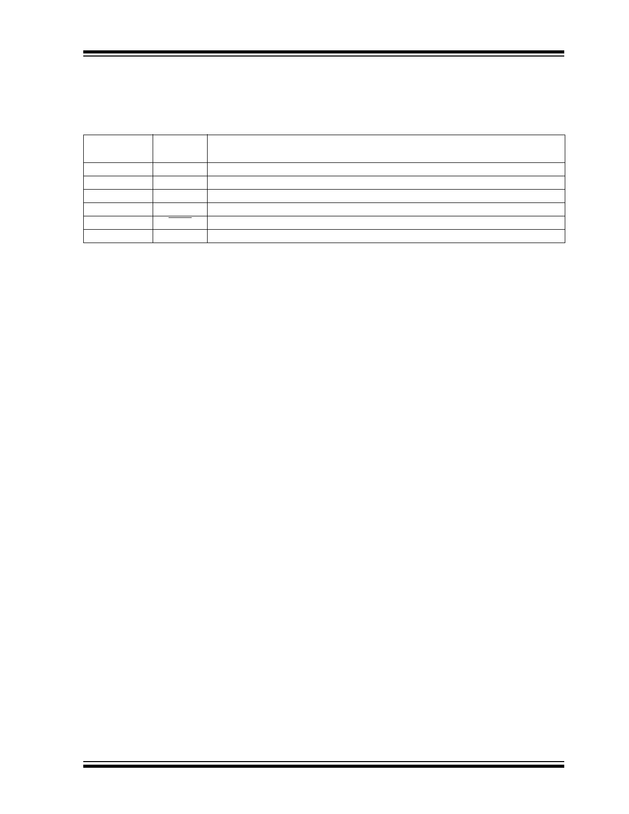
2.0
PIN DESCRIPTIONS
The descriptions of the pins are listed in Table 2-1.
TABLE 2-1:
PIN FUNCTION TABLE
Pin No.
(6-Pin SOT-23A)
Symbol
Description
1
OUT
Inverting charge pump output.
2
V
IN
Positive power supply input.
3
C
–
Commutation capacitor negative terminal.
4
GND
Ground.
5
SHDN
Shutdown input (active low).
6
C
+
Commutation capacitor positive terminal.
TC1221/TC1222
DS20001367C-page 4
2002-2014 Microchip Technology Inc.
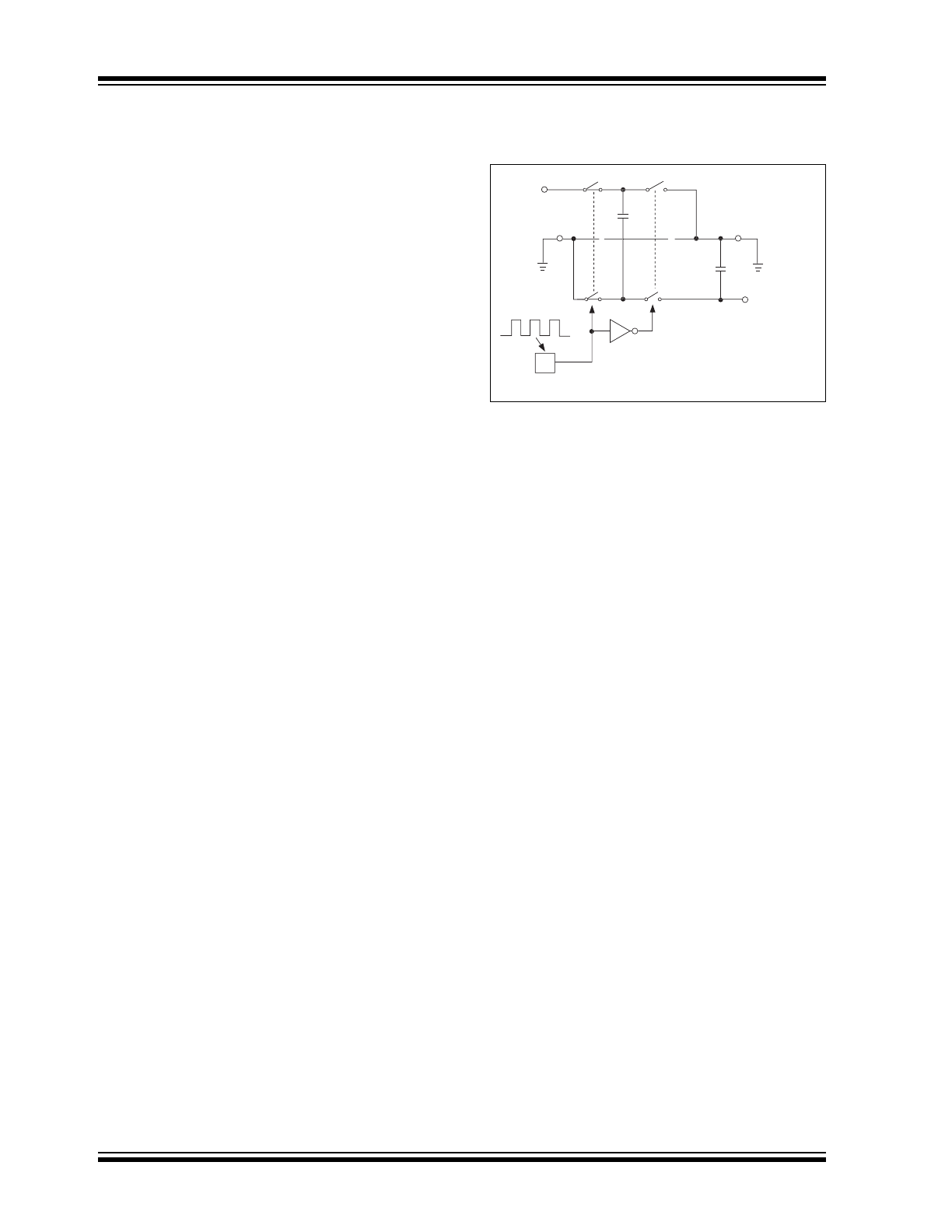
3.0
DETAILED DESCRIPTION
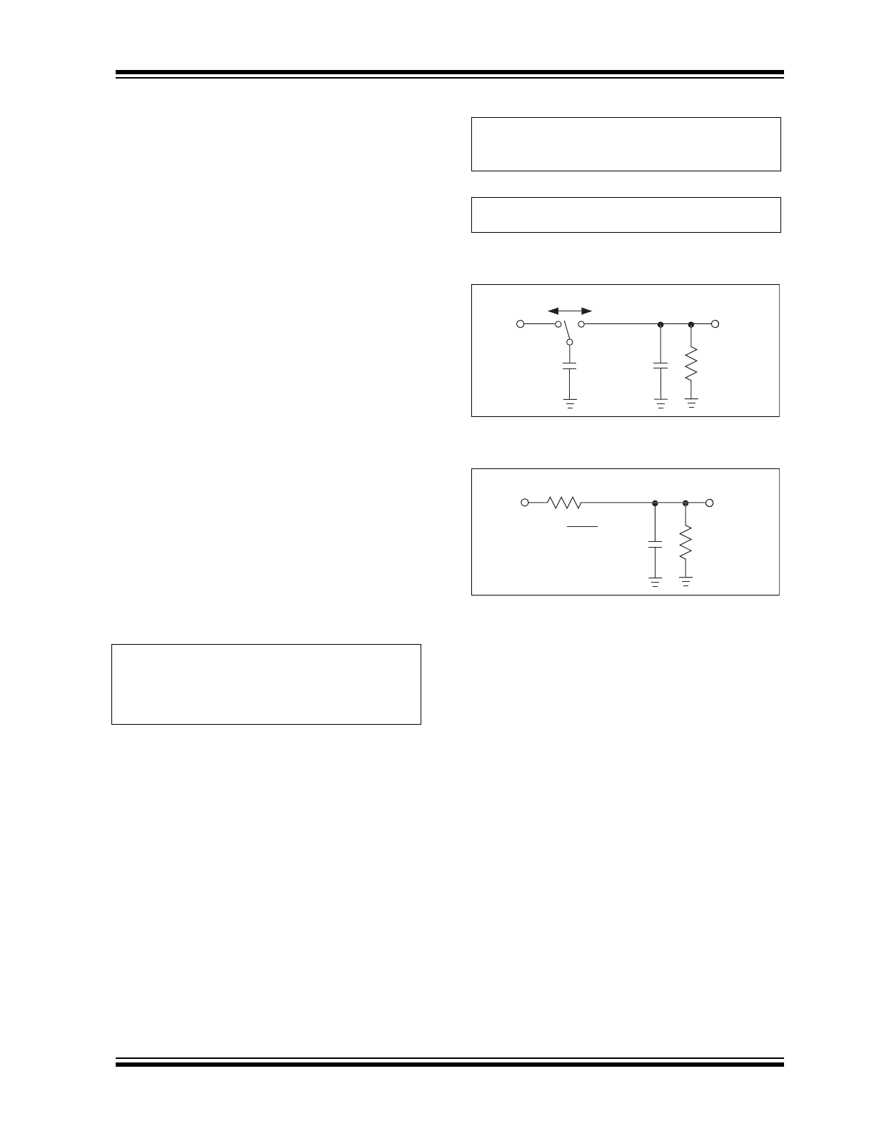
The TC1221/TC1222 charge pump converters invert
the voltage applied to the V
IN
pin. Conversion consists
of a two-phase operation (Figure 3-1). During the first
phase, switches S2 and S4 are opened and S1 and S3
are closed. During this time, C1 charges to the voltage
on V
IN
and load current is supplied from C2. During the
second phase, S2 and S4 are closed, and S1 and S3
are opened. This action connects C1 across C2,
restoring charge to C2.
FIGURE 3-1:
IDEAL SWITCHED
CAPACITOR CHARGE
PUMP
V
OUT
= – (V
IN
)
C1
C2
TC1221/1222
Phase 1
V
IN
S1
S3
S4
S2
OSC
2002-2014 Microchip Technology Inc.
DS20001367C-page 5
TC1221/TC1222
4.0
APPLICATIONS INFORMATION
4.1
Output Voltage Considerations
The TC1221/TC1222 perform voltage conversion but
do not provide regulation. The output voltage will droop
in a linear manner with respect to load current. The
value of this equivalent output resistance is approxi-
mately 25
nominal at +25°C and V
IN
= +5V. V
OUT
is
approximately -5V at light loads, and droops according
to the equation below:
V
DROP
= I
OUT
x R
OUT
V
OUT
= – (V
IN
– V
DROP
)
4.2
Charge Pump Efficiency
The overall power efficiency of the charge pump is
affected by four factors:
1.
Losses from power consumed by the internal
oscillator, switch drive, etc. (which vary with
input voltage, temperature and oscillator
frequency).
2.
I
2
R losses due to the on-resistance of the
MOSFET switches on-board the charge pump.
3.
Charge pump capacitor losses due to effective
series resistance (ESR).
4.
Losses that occur during charge transfer (from
the commutation capacitor to the output
capacitor) when a voltage difference between
the two capacitors exists.
Most of the conversion losses are due to factors (2) and
(3) above. These losses are given by Equation 4-1(b).
EQUATION 4-1:
The 1/(f
OSC
)(C1) term in Equation 4-1(b) is the
effective output resistance of an ideal switched
capacitor circuit (Figure 4-1 and Figure 4-2). The value
of R
SWITCH
can be approximated at 0.5
for the
TC1221/TC1222.
The remaining losses in the circuit are due to factor (4)
above, and are shown in Equation 4-2. The output
voltage ripple is given by Equation 4-3.
EQUATION 4-2:
EQUATION 4-3:
FIGURE 4-1:
IDEAL SWITCHED
CAPACITOR MODEL
FIGURE 4-2:
EQUIVALENT OUTPUT
RESISTANCE
4.3
Capacitor Selection
In order to maintain the lowest output resistance and
output ripple voltage, it is recommended that low ESR
capacitors be used. Additionally, larger values of C1
will lower the output resistance and larger values of
C2 will reduce output ripple. (Equation 4-1(b) and
Equation 4-3).
a) P
LOSS
(2, 3)
= I
OUT
2
x R
OUT
b) where R
OUT
=
[
1 / [f
OSC
(C1) ] + 8R
SWITCH
+
4ESR
C
1
+ ESR
C
2
]
P
LOSS
(4)
=
[
(0.5)(C1)(V
IN
2
– V
OUT
2
) + (0.5)
(C
2
)(V
RIPPLE
2
– 2V
OUT
V
RIPPLE
)
]
x f
OSC
V
RIPPLE
= [ I
OUT
/ 2 x ( f
OSC
) (C2)] + 2 ( I
OUT
) (ESR
C2
)
V+
V
OUT
R
L
C2
C1
f
V+
V
OUT
R
EQUIV
R
EQUIV
=
R
L
C2
f x C1
1
TC1221/TC1222
DS20001367C-page 6
2002-2014 Microchip Technology Inc.
Table 4-1 shows various values of C1 and the
corresponding output resistance values @ +25°C. It
assumes a 0.1
ESR
C1
and 2
R
SWITCH
. Table 4-2
shows the output voltage ripple for various values of
C2. The V
RIPPLE
values assume 10mA output load
current and 0.1
ESR
C2
.
TABLE 4-1:
OUTPUT RESISTANCE
VS. C1 (ESR = 0.1
)
TABLE 4-2:
OUTPUT VOLTAGE RIPPLE
VS. C2 (ESR = 0.1
)
I
OUT
10mA
4.4
Input Supply Bypassing
The V
IN
input should be capacitively bypassed to
reduce AC impedance and minimize noise effects due
to the internal switching of the device. The recom-
mended capacitor depends on the configuration of the
TC1221/TC1222.
4.5
Shutdown Input
The TC1221/TC1222 is enabled when SHDN is high,
and disabled when SHDN is low. This input cannot be
allowed to float. The SHDN input should be limited to
0.5V above V
IN
to avoid significant current flows.
4.6
Voltage Inverter
The most common application for charge pump
devices is the inverter (Figure 4-3). This application
uses two external capacitors: C1 and C2 (plus a power
supply bypass capacitor, if necessary). The output is
equal to -V
IN
plus any voltage drops due to loading.
Refer to Table 4-1 and Table 4-2 for capacitor
selection.
FIGURE 4-3:
VOLTAGE INVERTER
TEST CIRCUIT
C1 (
F)
TC1221
R
OUT
(
)
TC1222
R
OUT
(
)
0.22
52.9
22.6
0.33
40.8
20.5
0.47
33.5
19.4
1.0
25
17.8
C2 (
F)
TC1221
V
RIPPLE
(mV)
TC1222
V
RIPPLE
(mV)
0.22
184
32
0.33
123
22
0.47
87
16
1.0
42
9
3
2
4
5
1
C3
C1
C2
V
IN
V
OUT
R
L
TC1221
TC1220
C1–
IN
OUT
C1+
GND
Device
C1
C2
C3
TC1221 1
μF 1μF 1μF
TC1222 0.22
μF 0.22μF 0.22μF
SHDN
6
+
+
+
2002-2014 Microchip Technology Inc.
DS20001367C-page 7
TC1221/TC1222
4.7
Cascading Devices
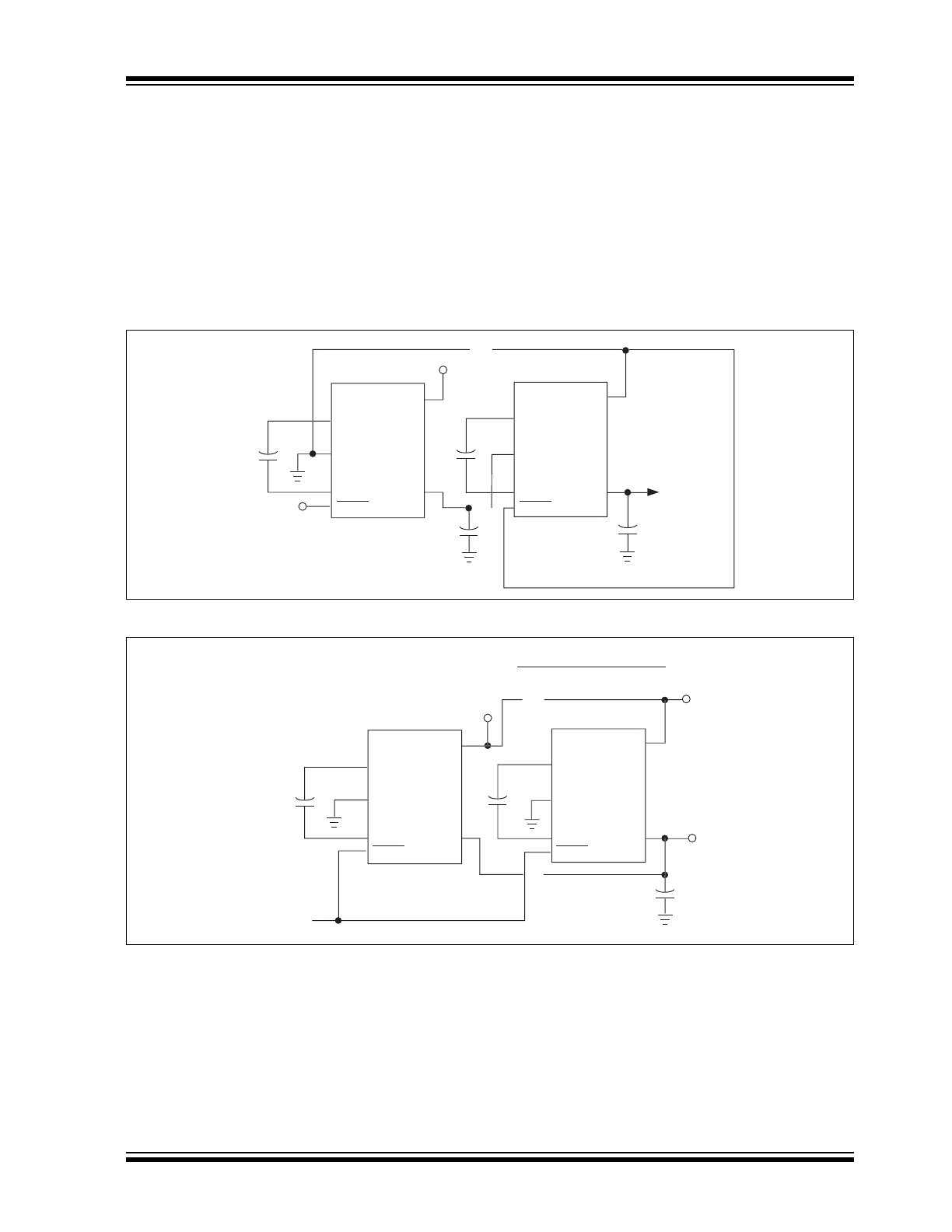
Two or more TC1221/TC1222 can be cascaded to
increase output voltage (Figure 4-4). If the output is
lightly loaded, it will be close to (-2 x V
IN
) but will droop
at least by R
OUT
of the first device multiplied by the I
Q
of the second. It can be seen that the output resistance
rises rapidly for multiple cascaded devices.
4.8
Paralleling Devices
To reduce the value of R
OUT
, multiple TC1221/
TC1222’s can be connected in parallel (Figure 4-5).
The output resistance will be reduced by a factor of N
where N is the number of TC1221/TC1222. Each
device will require its own pump capacitor (C1), but all
devices may share one reservoir capacitor (C2).
However, to preserve ripple performance the value of
C2 should be scaled according to the number of
paralleled TC1221/TC1222.
FIGURE 4-4:
CASCADING MULTIPLE DEVICES TO INCREASE OUTPUT VOLTAGE
FIGURE 4-5:
PARALLELING MULTIPLE DEVICES TO REDUCE OUTPUT RESISTANCE
C1
C1
C2
6
6
4
3
4
1
2
2
1
3
C2
V
IN
V
OUT
V
OUT
= -nV
IN
TC1221
TC1222
TC1221
TC1222
. . .
. . .
SHDN
SHDN
V
IN
5
5
"1"
"n"
+
+
+
+
C1
C1
6
5
4
3
4
1
2
2
1
3
C2
V
OUT
V
OUT
= -V
IN
R
OUT
= R
OUT
OF SINGLE DEVICE
V
IN
NUMBER OF DEVICES
TC1221
TC1222
TC1221
TC1222
. . .
. . .
SHDN
SHDN
Shutdown
Control
5
6
V
IN
+
+
+
"1"
"n"
TC1221/TC1222
DS20001367C-page 8
2002-2014 Microchip Technology Inc.
4.9
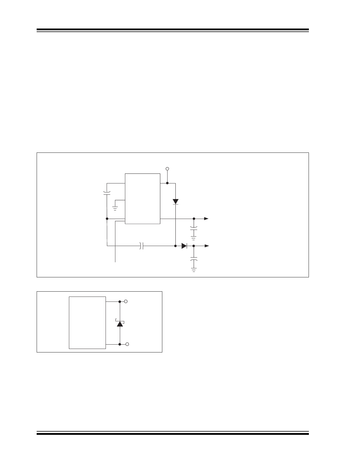
Voltage Doubler/Inverter
Another common application of the TC1221/TC1222 is
shown in Figure 4-6. This circuit performs two functions
in combination. C1 and C2 form the standard inverter
circuit described above. C3 and C4 plus the two diodes
form the voltage doubler circuit. C1 and C3 are the
pump capacitors and C2 and C4 are the reservoir
capacitors. Because both sub-circuits rely on the same
switches if either output is loaded, both will droop
toward GND. Make sure that the total current drawn
from both the outputs does not total more than 40mA.
4.10
Diode Protection for Heavy Loads
When heavy loads require the OUT pin to sink large
currents being delivered by a positive source, diode
protection may be needed. The OUT pin should not be
allowed to be pulled above ground. This is
accomplished by connecting a Schottky diode
(1N5817) as shown in Figure 4-7.
4.11
Layout Considerations
As with any switching power supply circuit, good layout
practice is recommended. Mount components as close
together as possible to minimize stray inductance and
capacitance. Noise leakage into other circuitry can be
minimized with the use of a large ground plane.
FIGURE 4-6:
COMBINED DOUBLER AND INVERTER
FIGURE 4-7:
HIGH V– LOAD CURRENT
C1
D1
D2
D1, D2 = 1N4148
6
4
1
2
3
C2
C4
C3
V
IN
V
OUT
= -V
IN
V
OUT
= (2V
IN
) –
(V
FD1
) – (V
FD2
)
TC1221
TC1222
Shutdown
Control
5
+
+
+
+
TC1221
TC1222
GND
OUT
4
1
2002-2014 Microchip Technology Inc.
DS20001367C-page 9
TC1221/TC1222
5.0
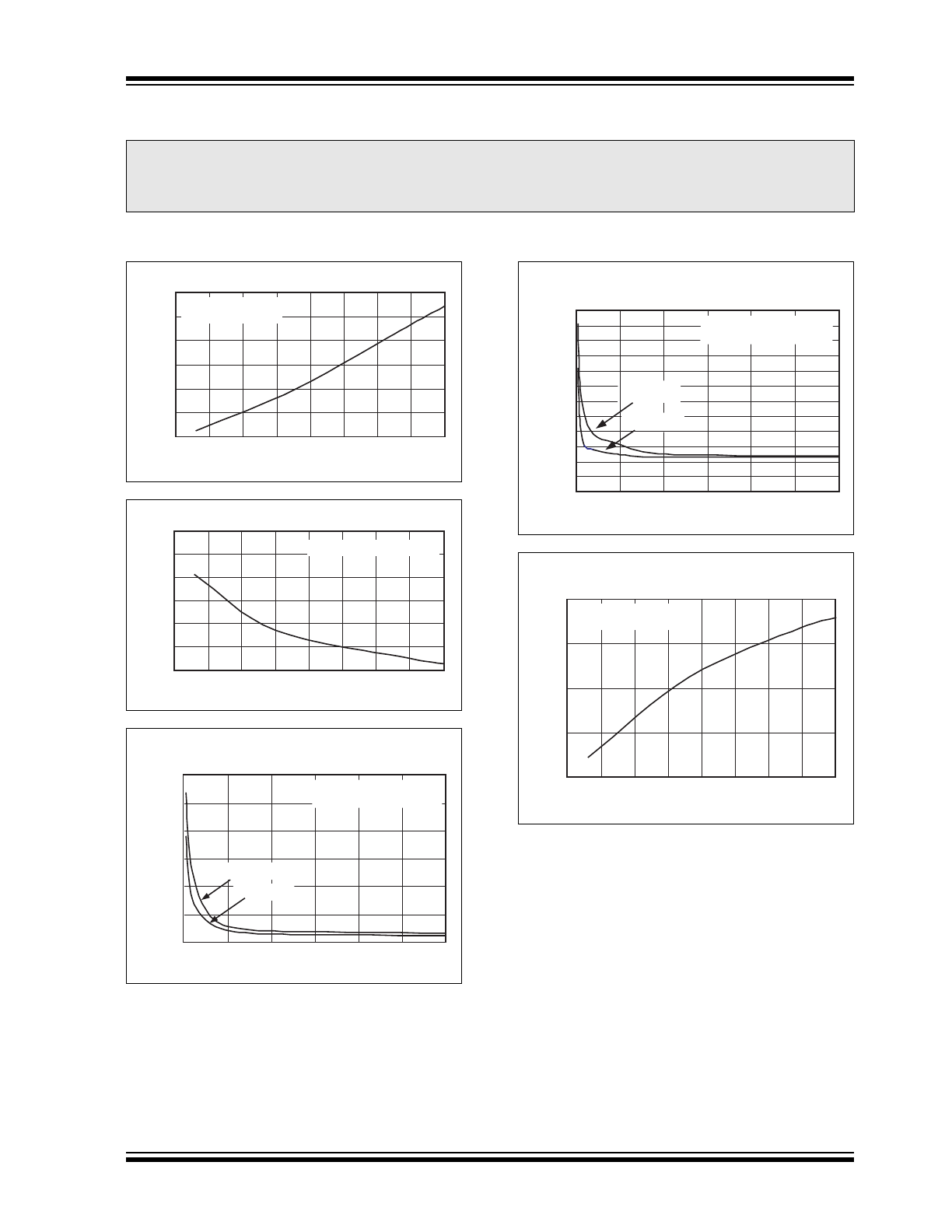
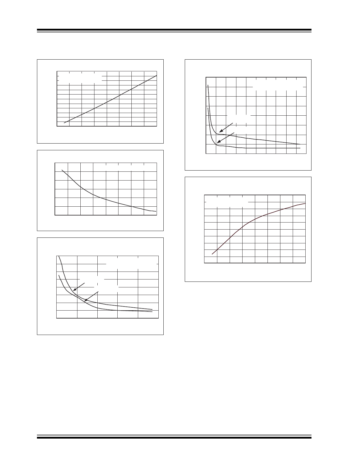
TYPICAL CHARACTERISTICS
Circuit of Figure 4-3, V
IN
= +5V, C1 = C2 = C3, T
A
= 25°C unless otherwise noted.
Note:
The graphs and tables provided following this note are a statistical summary based on a limited number of
samples and are provided for informational purposes only. The performance characteristics listed herein are
not tested or guaranteed. In some graphs or tables, the data presented may be outside the specified
operating range (e.g., outside specified power supply range) and therefore outside the warranted range.
TC1221 Supply Current vs. Supply Voltage
50
100
150
200
250
300
350
1.5
2.0
2.5
3.0
3.5
4.0
4.5
5.0
SUPPLY VOLTAGE (V)
SUPPLY CURRENT
(μ
A)
C1 = C2 = C3 = 1
μF,
RL =
∞, +25°C
5.5
TC1221 Output Resistance vs. Supply Voltage
35
40
45
50
55
60
65
1.5
2.0
2.5
3.0
3.5
4.0
4.5
5.0
5.5
SUPPLY VOLTAGE (V)
OUTPUT RESISTANCE
(O
h
m
s
)
C1 = C2 = C3 = 1
μF, +25°C
TC1221 Output Voltage Ripple
vs. Capacitance, C
2
0
50
100
150
200
250
300
0
5
10
15
CAPACITANCE (
μF)
OUTPUT VOLTAGE RIPPLE
(m
Vp
-p
)
V
IN
= 5.0V
V
IN
= 3.3V
V
IN
= 3.3V, RL = 1K, +25
°C
V
IN
= 5.0V, RL = 1K, +25
°C
OUTPUT VOLTAGE DROOP
(m
V)
V
IN
= 5.0V
0
100
200
300
400
500
600
0
5
10
15
TC1221 Output Voltage Droop
vs. Capacitance, C
1
= C
2
V
IN
= 3.3V
V
IN
= 3.3V, RL = 1K, +25
°C
V
IN
= 5.0V, RL = 1K, +25
°C
CAPACITANCE (
μF)
TC1221 Oscillator Frequency
vs. Supply Voltage
90
100
110
120
130
1.5
2.0
2.5
3.0
3.5
4.0
4.5
5.0
5.5
OSCILLATOR FREQUENCY (kH
z
)
SUPPLY VOLTAGE (V)
C1 = C2 = C3 = 1
μF,
RL =
∞, +25°C
TC1221/TC1222
DS20001367C-page 10
2002-2014 Microchip Technology Inc.
5.0
TYPICAL CHARACTERISTICS (CONTINUED)
TC1222 Supply Current vs. Supply Voltage
250
500
750
1000
1250
1500
1750
1.5
2.0
2.5
3.0
3.5
4.0
4.5
5.0
5.5
SUPPLY VOLTAGE (V)
SUPPLY CURRENT
(μ
A)
C1 = C2 = C3 = 0.22
μF,
RL =
∞, +25°C
TC1222 Output Resistance vs. Supply Voltage
35
40
45
50
55
60
65
1.5
2.0
2.5
3.0
3.5
4.0
4.5
5.0
5.5
OUTPUT RESISTANCE (Oh
m
s
)
SUPPLY VOLTAGE (V)
C1 = C2 = C3 = 0.22
μF, +25°C
0
40
80
120
0
1
2
3
4
5
160
TC1222 Output Voltage Ripple
vs. Capacitance , C
2
V
IN
= 5.0V
V
IN
= 3.3V
V
IN
= 3.3V, RL = 1K, +25
°C
V
IN
= 5.0V, RL = 1K, +25
°C
CAPACITANCE (
μF)
OUTPUT VOLTAGE RIPPLE
(m
Vp
-p
)
V
IN
= 5.0V
TC1222 Output Voltage Droop
vs. Capacitance, C
1
= C
2
V
IN
= 3.3V
100
150
200
250
300
350
400
450
500
0
1
2
3
4
5
CAPACITANCE (
μF)
OUTPUT VOLTAGE DROOP
(m
V)
V
IN
= 3.3V, RL = 1K, +25
°C
V
IN
= 5.0V, RL = 1K, +25
°C
500
550
600
650
700
750
1.5
2.0
2.5
3.0
3.5
4.0
4.5
5.0
5.5
OSCILLATOR FREQUENCY
(kH
z
)
TC1222 Oscillator Frequency
vs. Supply Voltage
SUPPLY VOLTAGE (V)
C1 = C2 = C3 = 0.22
μF,
RL =
∞, +25°C