
2006-2014 Microchip Technology Inc.
DS20001358D-page 1
TC1121
Features:
• Optional High-Frequency Operation Allows Use of
Small Capacitors
• Low Operating Current (FC = Open):
- 50
A
• High Output Current (100 mA)
• Converts a 2.4V to 5.5V Input Voltage to a
Corresponding Negative Output Voltage
(Inverter mode)
• Uses Only 2 Capacitors; No Inductors Required
• Selectable Oscillator Frequency:
- 10 kHz to 200 kHz
• Power-Saving Shutdown Input
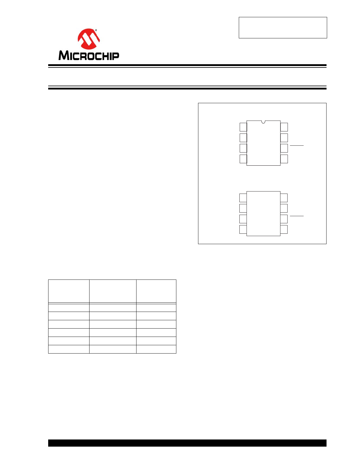
• Available in 8-Pin MSOP, 8-Pin PDIP and 8-Pin
Small Outline (SOIC) Packages
Applications:
• Laptop Computers
• Medical Instruments
• Disk Drives
•
P-Based Controllers
• Process Instrumentation
Device Selection Table
Package Type
General Description:
The TC1121 is a charge pump converter with 100 mA
output current capability. It converts a 2.4V to 5.5V
input to a corresponding negative output voltage. As
with all charge pump converters, the TC1121 uses no
inductors saving cost, size and EMI.
An on-board oscillator operates at a typical frequency
of 10 kHz (at V
+
= 5V) when the frequency control input
(FC) is left open. The oscillator frequency increases to
200 kHz when FC is connected to V
+
, allowing the use
of smaller capacitors. Operation at sub-10 kHz
frequencies results in lower quiescent current and is
accomplished with the addition of an external capacitor
from OSC (pin 7) to ground. The TC1121 also can be
driven from an external clock connected OSC. Typical
supply current at 10 kHz is 50
A, and falls to less than
1
A when the shutdown input is brought low, whether
the internal or an external clock is used. The TC1121 is
available in 8-pin SOIC, MSOP and PDIP packages.
Part
Number
Package
Operating
Temp.
Range
TC1121COA
8-Pin SOIC
0°C to +70°C
TC1121CPA
8-Pin PDIP
0°C to +70°C
TC1121CUA
8-Pin MSOP
0°C to +70°C
TC1121EOA
8-Pin SOIC
-40°C to +85°C
TC1121EPA
8-Pin PDIP
-40°C to +85°C
TC1121EUA
8-Pin MSOP
-40°C to +85°C
TC1121COA
TC1121EOA
TC1121CUA
TC1121EUA
SHDN
FC
CAP
+
CAP
–
1
2
3
4
8
7
6
5
GND
OSC
V+
8-Pin SOIC
8-Pin MSOP
V
OUT
TC1121CPA
TC1121EPA
SHDN
FC
CAP
+
CAP
–
1
2
3
4
8
7
6
5
GND
OSC
V+
8-Pin PDIP
V
OUT
100mA Charge Pump Voltage Converter with Shutdown
Obsolete Device
TC1121
DS20001358D-page 2
2006-2014 Microchip Technology Inc.
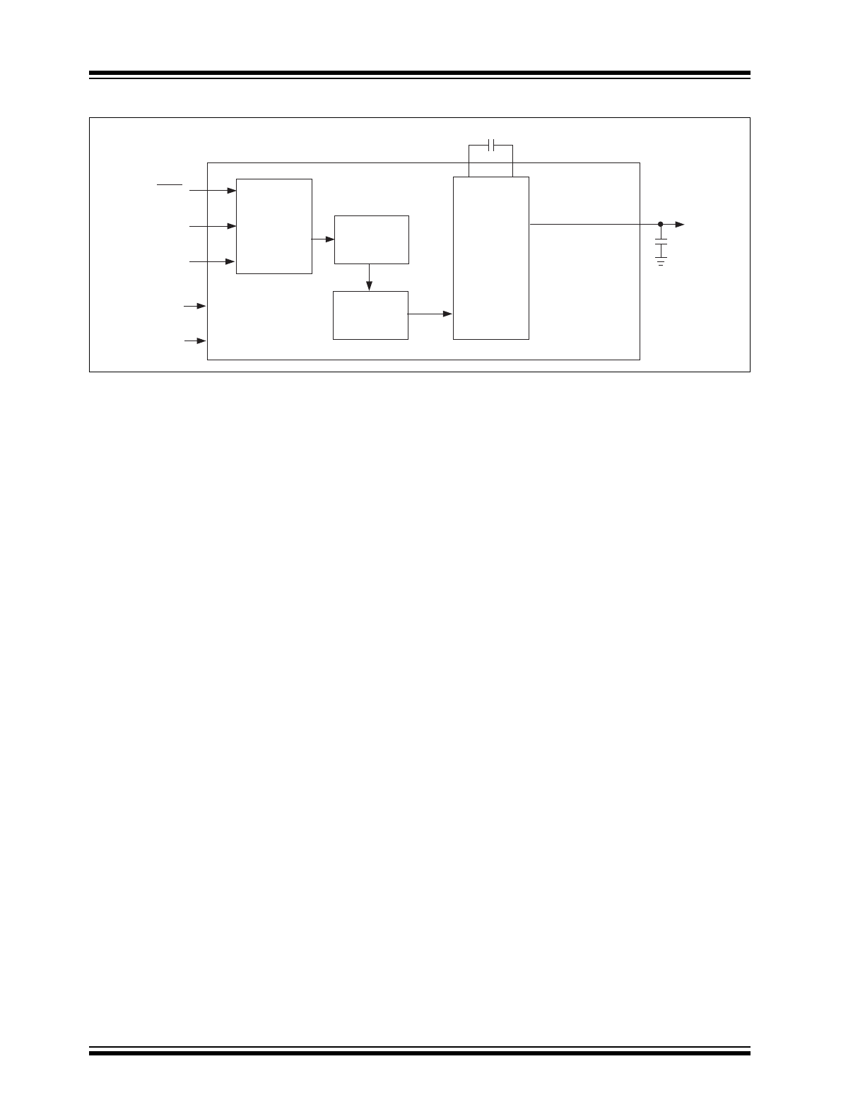
Functional Block Diagram
SHDN
TC1121
OSC
Control
FC
OSC
GND
V+
V
OUT
Switch
Matrix
RC
Oscillator
Logic
Circuits
C2
CAP+
C1
CAP–
+
–
+
2006-2014 Microchip Technology Inc.
DS20001358D-page 3
TC1121
1.0
ELECTRICAL
CHARACTERISTICS
Absolute Maximum Ratings*
Supply Voltage (V
DD
) ............................................... 6V
OSC, FC, SHDN Input Voltage ..... -0.3V to (V
+
+ 0.3V)
Output Short Circuit Duration ........................... 10 Sec.
Package Power Dissipation (T
A
70°C)
8-Pin PDIP .............................................. 730 mW
8-Pin SOIC .............................................. 470 mW
8-Pin MSOP ............................................ 333 mW
Operating Temperature Range
C Suffix............................................ 0°C to +70°C
E Suffix......................................... -40°C to +85°C
Storage Temperature Range .............. -65°C to +150°C
*Stresses above those listed under “Absolute
Maximum Ratings” may cause permanent damage to
the device. These are stress ratings only and functional
operation of the device at these or any other conditions
above those indicated in the operation sections of the
specifications is not implied. Exposure to Absolute
Maximum Rating conditions for extended periods may
affect device reliability.
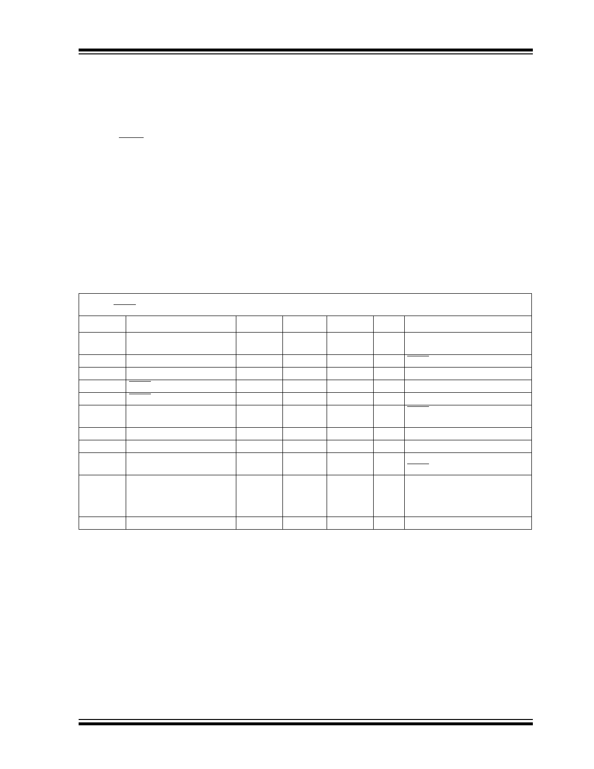
TC1121 ELECTRICAL SPECIFICATIONS
Electrical Characteristics: T
A
= 0°C to 70°C (C suffix), -40°C to +85°C (E suffix), V
+
= 5V ±10% C
OSC
= Open, C1, C2 = 10
F,
FC = V
+
, SHDN = V
IH
, typical values are at T
A
= 25°C unless otherwise noted.
Symbol
Parameter
Min.
Typ.
Max.
Units
Test Conditions
I
DD
Active Supply Current
—
—
50
0.6
100
1
A
mA
R
L
= Open, FC = Open or GND
R
L
= Open, FC = V
+
I
SHUTDOWN
Shutdown Supply Current
—
0.2
1.0
A
SHDN = 0V
V
+
Supply Voltage
2.4
—
5.5
V
V
IH
SHDN Input Logic High
V
DD
x 0.8
—
—
V
V
IL
SHDN Input Logic Low
—
—
0.4
V
I
IN
Input Leakage Current
-1
-4
—
—
1
4
A
SHDN, OSC
FC pin
R
OUT
Output Source Resistance
—
12
20
I
OUT
= 60 mA
I
OUT
Output Current
60
100
—
mA
V
OUT
= more negative than -3.75V
F
OSC
Oscillator Frequency
5
100
10
200
—
—
kHz
Pin 7 Open, Pin 1 Open or GND
SHDN = V
IH
, Pin 1 = V
+
P
EFF
Power Efficiency
—
93
94
—
—
97
97
92
—
—
—
%
FC = GND for all
R
L
= 2k between V
+
and V
OUT
R
L
= 1k
between V
OUT
and GND
I
L
= 60 mA to GND
V
EFF
Voltage Conversion Efficiency
99
99.9
—
%
R
L
= Open
Note
1:
Connecting any input terminal to voltages greater than V
+
or less than GND may cause destructive latch-up. It is recommended that no
inputs from sources operating from external supplies be applied prior to “power up” of the TC1121.
TC1121
DS20001358D-page 4
2006-2014 Microchip Technology Inc.
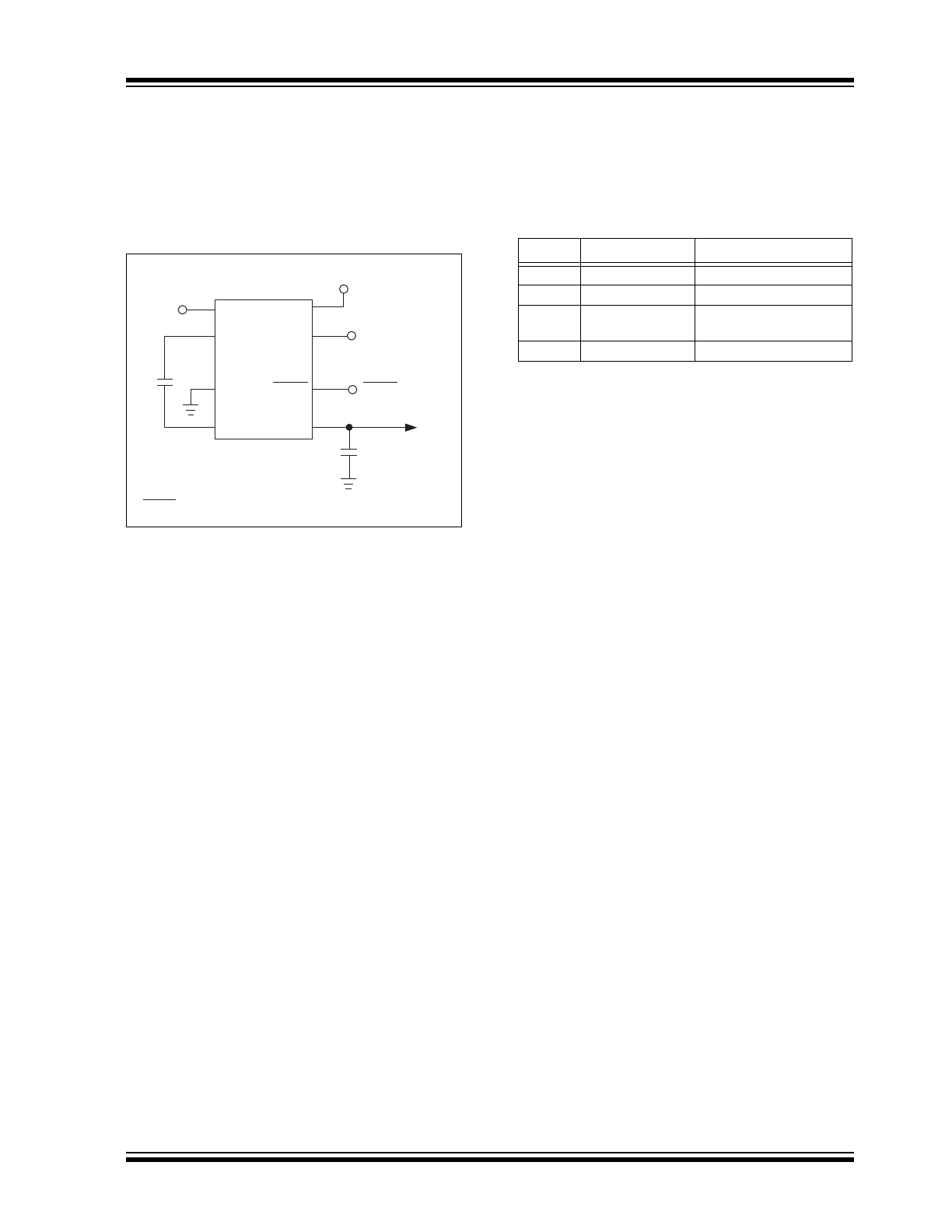
2.0
PIN DESCRIPTIONS
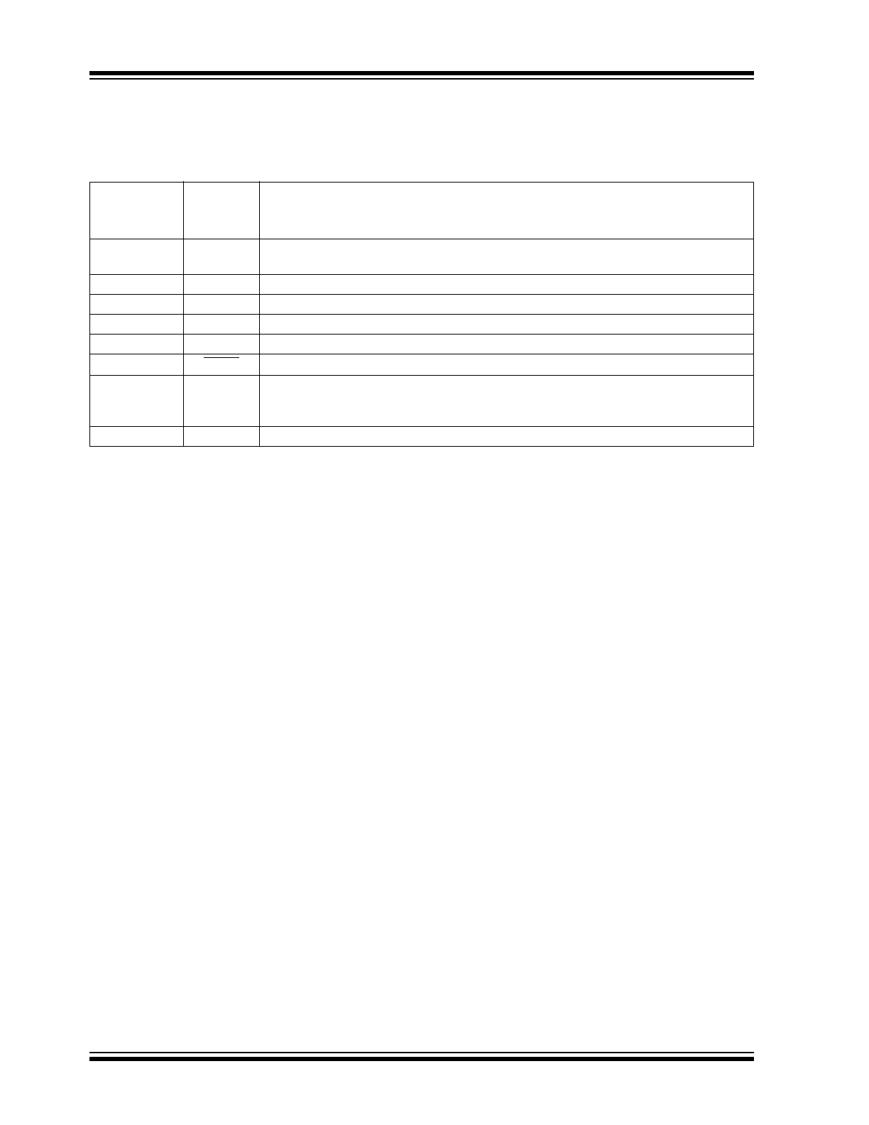
The descriptions of the pins are listed in Table 2-1.
TABLE 2-1:
PIN FUNCTION TABLE
Pin No.
(8-Pin MSOP,
PDIP, SOIC)
Symbol
Description
1
FC
Frequency control for internal oscillator, FC = open, F
OSC
= 10 kHz typ; FC = V
+
, F
OSC
= 200 kHz typ; FC has no effect when OSC pin is driven externally.
2
CAP
+
Charge-pump capacitor, positive terminal.
3
GND
Power-supply ground input.
4
CAP
–
Charge-pump capacitor, negative terminal.
5
OUT
Output, negative voltage.
6
SHDN
Shutdown.
7
OSC
Oscillator control input. An external capacitor can be added to slow the oscillator. Take
care to minimize stray capacitance. An external oscillator also may be connected to
overdrive OSC.
8
V
+
Power-supply positive voltage input.
2006-2014 Microchip Technology Inc.
DS20001358D-page 5
TC1121
3.0
APPLICATIONS
3.1
Negative Voltage Converter
The TC1121 is typically used as a charge-pump voltage
inverter. C1 and C2 are the only two external capacitors
used in the operating circuit (Figure 3-1).
FIGURE 3-1:
Charge Pump Inverter
The TC1121 is not sensitive to load current changes,
although its output is not actively regulated. A typical
output source resistance of 11.8
means that an input
of +5V results in -5V output voltage under light load,
and only decreases to -3.8V typ with a 100 mA load.
The supplied output current is from capacitor C2 during
one-half the charge-pump cycle. This results in a
peak-to-peak ripple of:
V
RIPPLE
= I
OUT
/2(f
PUMP
) (C2) + I
OUT
(ESR
C2
)
Where f
PUMP
is 5 kHz (one half the nominal 10 kHz
oscillator frequency), and C2 = 150
F with an ESR of
0.2
, ripple is about 90 mV with a 100 mA load current.
If C2 is raised to 390
F, the ripple drops to 45 mV.
3.2
Changing Oscillator Frequency
The TC1121’s clock frequency is controlled by four
modes:
TABLE 3-1:
OSCILLATOR FREQUENCY
MODES
The oscillator runs at 10 kHz (typical) when FC and
OSC are not connected. The oscillator frequency is
lowered by connecting a capacitor between OSC and
GND, but FC can still multiply the frequency by 20
times in this mode.
An external clock source that swings within 100 mV of
V
+
and GND may overdrive OSC in the Inverter mode.
OSC can be driven by any CMOS logic output. When
OSC is overdriven, FC has no effect.
Note that the frequency of the signal appearing at
CAP
+
and CAP
–
is half that of the oscillator. In addition,
by lowering the oscillator frequency, the effective
output resistance of the charge-pump increases. To
compensate for this, the value of the charge-pump
capacitors may be increased.
Because the 5 kHz output ripple frequency may be low
enough to interfere with other circuitry, the oscillator
frequency can be increased with the use of the FC pin
or an external oscillator. The output ripple frequency is
half the selected oscillator frequency. Although the
TC1121’s quiescent current will increase if the clock
frequency is increased, it allows smaller capacitance
values to be used for C1 and C2.
3.3
Capacitor Selection
In addition to load current, the following factors affect
the TC1121 output voltage drop from its ideal value 1)
output resistance, 2) pump (C1) and reservoir (C2)
capacitor ESRs and 3) C1 and C2 capacitance.
The voltage drop is the load current times the output
resistance. The loss in C2 is the load current times C2’s
ESR; C1’s loss is larger because it handles currents
greater than the load current during charge-pump
operation. Therefore, the voltage drop due to C1 is
about four times C1’s ESR multiplied by the load
current, and a low (or high) ESR capacitor has a
greater impact on performance for C1 than for C2.
In general, as the TC1121’s pump frequency increases,
capacitance values needed to maintain comparable
ripple and output resistance diminish proportionately.
4
3
6
7
8
5
2
1
C1
C2
2.4V to 5.5V
V
OUT
TC1121
GND
OSC
CAP
+
CAP
–
FC
V
OUT
V
IN
SHDN
*SHDN should be tied to V
IN
if not used.
SHDN*
+
–
+
–
FC
OSC
Oscillator Frequency
Open
Open
10 kHz
FC = V
+
Open
200 kHz
Open or
FC = V
+
External Capacitor
See Typical Operating
Characteristics
Open
External Clock
External Clock Frequency
TC1121
DS20001358D-page 6
2006-2014 Microchip Technology Inc.
3.4
Cascading Devices
To produce greater negative magnitudes of the initial
supply voltage, the TC1121 may be cascaded (see
Figure 3-2). Resulting output resistance is approxi-
mately equal to the sum of individual TC1121 R
OUT
values. The output voltage (where n is an integer
representing the number of devices cascaded) is
defined by V
OUT
= -n (V
IN
).
3.5
Paralleling Devices
To reduce output resistance, multiple TC1121s may be
paralleled (see Figure 3-3). Each device needs a pump
capacitor C1, but the reservoir capacitor C2 serves all
devices. The value of C2 should be increased by a
factor of n (the number of devices).
FIGURE 3-2:
Cascading TC1121s to Increase Output Voltage
FIGURE 3-3:
Paralleling TC1121s to Reduce Output Resistance
C1
C1n
4
4
3
2
3
5
8
8
7
5
2
C2
V
IN
+
C2n
TC1121
TC1121
GND
GND
OSC
OSC
CAP
+
CAP
+
CAP
–
CAP
–
FC
FC
SHDN
V
OUT
V
OUT
V
IN
V
OUT
V
IN
SHDN
SHDN*
SHDN*
“1”
“n”
+
+
+
+
*SHDN should be tied to V
IN if
not used.
C1
C1n
4
4
3
2
3
5
8
8
7
5
2
C2
V+
IN
TC1121
TC1121
GND
GND
OSC
OSC
CAP
+
CAP
+
CAP
–
CAP
–
FC
FC
SHDN
V
OUT
V
OUT
V
IN
V
IN
SHDN
SHDN*
SHDN*
*SHDN should be tied to V
IN if
not used.
“1”
“n”
+
+
+
7
OSC
R
OUT
= R
OUT
(of TC1121)/n(number of devices)
2006-2014 Microchip Technology Inc.
DS20001358D-page 7
TC1121
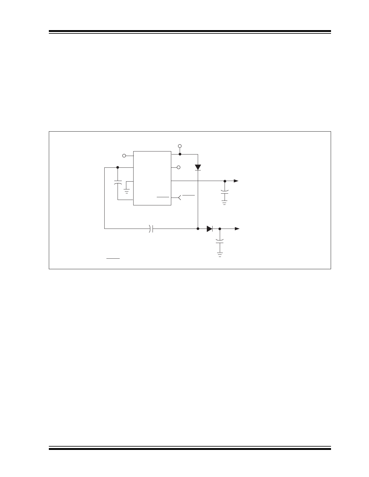
3.6
Combined Positive Supply
Multiplication and Negative
Voltage Conversion
Figure 3-4 shows this dual function circuit, in which
capacitors C1 and C2 perform pump and reservoir
functions to generate negative voltage. Capacitors C3
and C4 are the respective capacitors for multiplied
positive voltage. This particular configuration leads to
higher source impedances of the generated supplies
due to the finite impedance of the common
charge-pump driver.
FIGURE 3-4:
Combined Positive Multiplier and Negative Converter
C1
D1
D2
D1, D2 = 1N4148
4
3
6
8
5
2
C2
C4
C3
V
IN
+
V
OUT
= (
2V
IN
)
–
(V
FD1
)
–
(V
FD2
)
TC1121
GND
OSC
CAP
+
CAP
–
FC
SHDN
V
OUT
V
IN
SHDN*
V
OUT
=
V
IN
–
*SHDN should be tied to V
IN
if
not used.
+
+
+
+
TC1121
DS20001358D-page 8
2006-2014 Microchip Technology Inc.
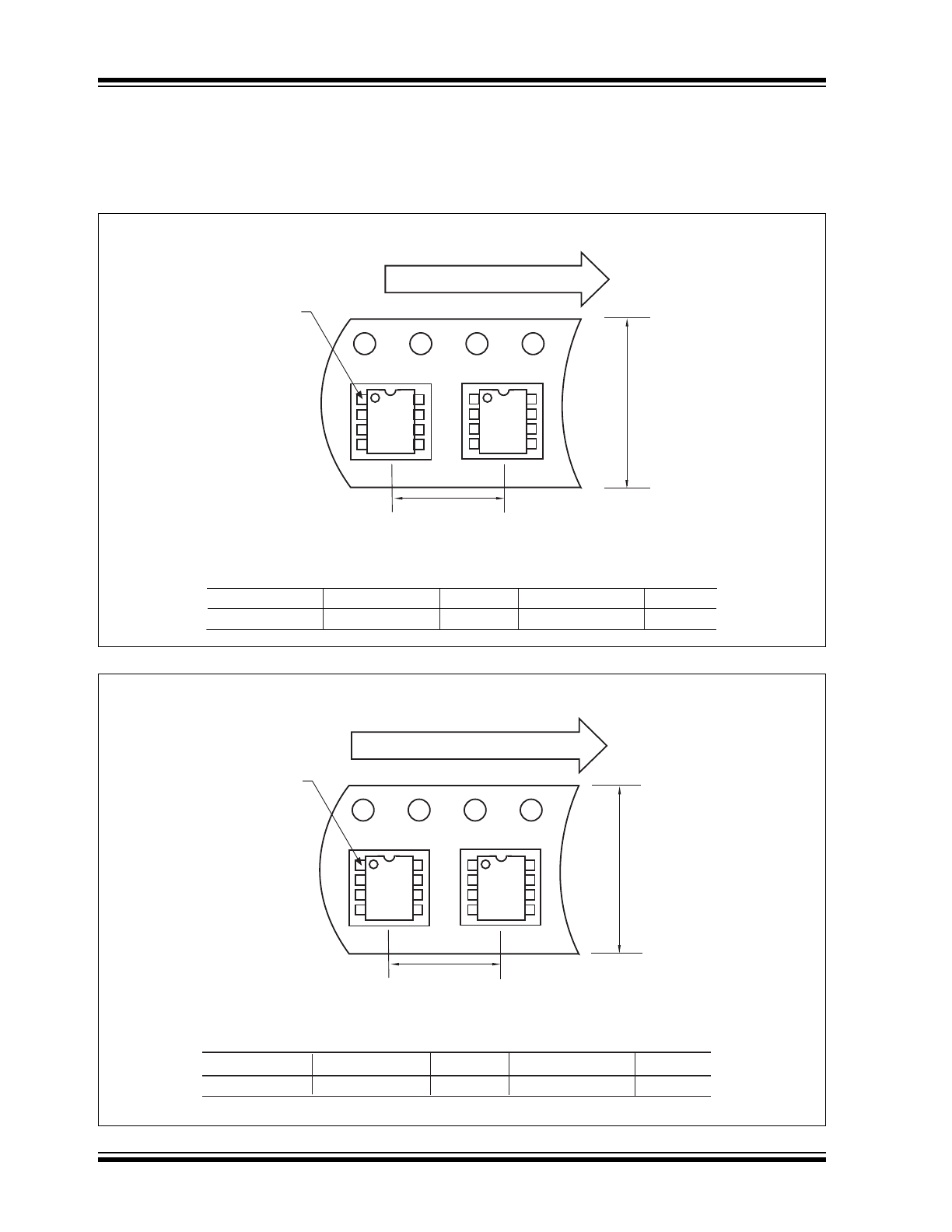
4.0
PACKAGING INFORMATION
4.1
Package Marking Information
Package marking data not available at this time.
4.2
Taping Form
Component Taping Orientation for 8-Pin MSOP Devices
Package
Carrier Width (W)
Pitch (P)
Part Per Full Reel
Reel Size
8-Pin MSOP
12 mm
8 mm
2500
13 in
Carrier Tape, Number of Components Per Reel and Reel Size
Pin 1
User Direction of Feed
Standard Reel Component Orientation
for 713 Suffix Device
W
P
Component Taping Orientation for 8-Pin SOIC (Narrow) Devices
Package
Carrier Width (W)
Pitch (P)
Part Per Full Reel
Reel Size
8-Pin SOIC (N)
12 mm
8 mm
2500
13 in
Carrier Tape, Number of Components Per Reel and Reel Size
Standard Reel Component Orientation
for 713 Suffix Device
Pin 1
User Direction of Feed
P
W
2006-2014 Microchip Technology Inc.
DS20001358D-page 9
TC1121
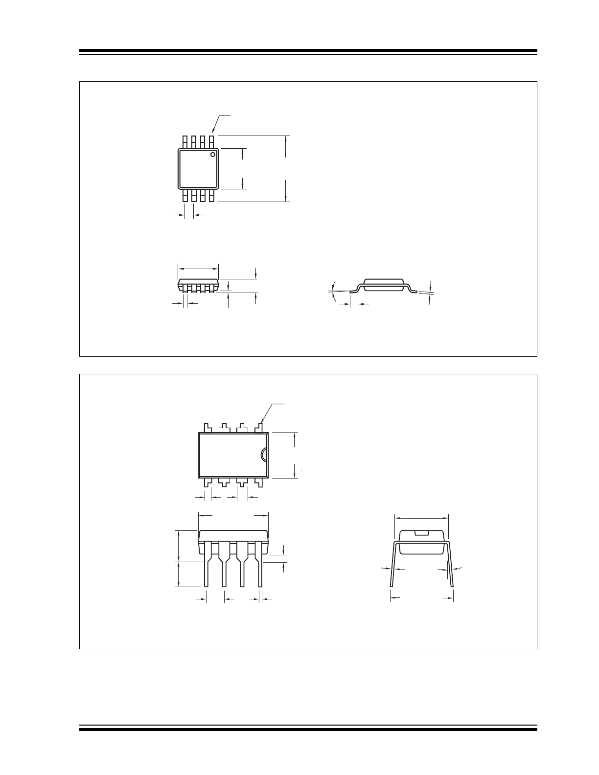
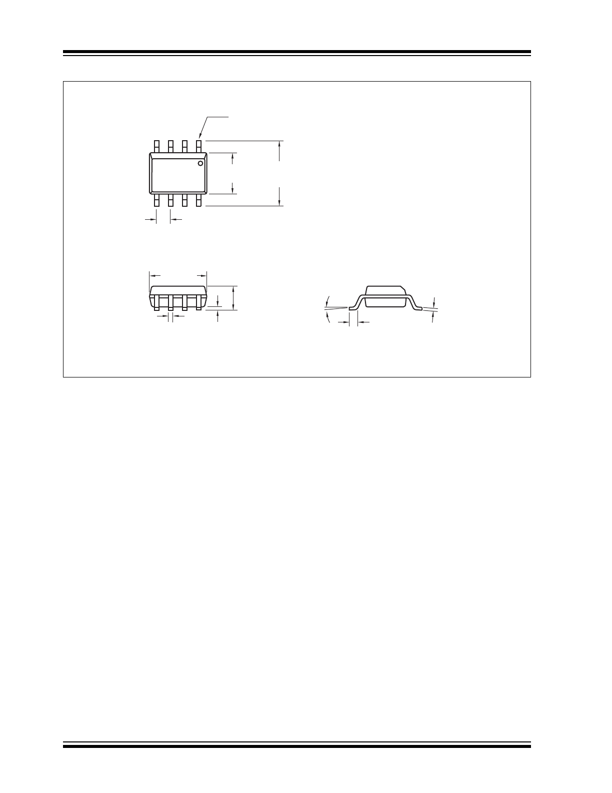
4.3
Package Dimensions
8-Pin MSOP
.122 (3.10)
.114 (2.90)
.122 (3.10)
.114 (2.90)
.043 (1.10)
Max.
.006
(0.15)
.002 (0.05)
.016 (0.40)
.010 (0.25)
.197 (5.00)
.189 (4.80)
.008 (0.20)
.005 (0.13)
.028 (0.70)
.016 (0.40)
6° Max.
.026 (0.65) Typ.
Pin 1
Dimensions: inches (mm)
3° Min.
Pin 1
.260 (6.60)
.240 (6.10)
.045 (1.14)
.030 (0.76)
.070 (1.78)
.040 (1.02)
.400 (10.16)
.348 (8.84)
.200 (5.08)
.140 (3.56)
.150 (3.81)
.115 (2.92)
.110 (2.79)
.090 (2.29)
.022 (0.56)
.015 (0.38)
.040 (1.02)
.020 (0.51)
.015 (0.38)
.008 (0.20)
.310 (7.87)
.290 (7.37)
.400 (10.16)
.310 (7.87)
8-Pin Plastic DIP
Dimensions: inches (mm)
TC1121
DS20001358D-page 10
2006-2014 Microchip Technology Inc.
Package Dimensions (Continued)
.050 (1.27) Typ.
8
°
Max.
Pin 1
.244 (6.20)
.228 (5.79)
.157 (3.99)
.150 (3.81)
.197 (5.00)
.189 (4.80)
.020 (0.51)
.013 (0.33)
.010 (0.25)
.004 (0.10)
.069 (1.75)
.053 (1.35)
.010 (0.25)
.007 (0.18)
.050 (1.27)
.016 (0.40)
8-Pin SOIC
Dimensions: inches (mm)