
2005-2013 Microchip Technology Inc.
DS21813F-page 1
TC1017
Features:
• Space-saving 5-Pin SC-70 and SOT-23 Packages
• Extremely Low Operating Current for Longer
Battery Life: 53 µA (typ.)
• Very Low Dropout Voltage
• Rated 150 mA Output Current
• Requires Only 1 µF Ceramic Output Capacitance
• High Output Voltage Accuracy:
0.5% (typical)
• 10 µs (typ.) Wake-Up Time from SHDN
• Power-Saving Shutdown Mode: 0.05 µA (typ.)
• Overcurrent and Overtemperature Protection
• Pin-Compatible Upgrade for Bipolar Regulators
Applications:
• Cellular/GSM/PHS Phones
• Battery-Operated Systems
• Portable Computers
• Medical Instruments
• Electronic Games
• Pagers
General Description:
The TC1017 is a high-accuracy (typically ±0.5%)
CMOS upgrade for bipolar Low Dropout regulators
(LDOs). It is offered in a SC-70 or SOT-23 package.
The SC-70 package represents a 50% footprint reduc-
tion versus the popular SOT-23 package and is offered
in two pinouts to make board layout easier.
Developed specifically for battery-powered systems,
the TC1017’s CMOS construction consumes only
53 µA typical supply current over the entire 150 mA
operating load range. This can be as much as 60 times
less than the quiescent operating current consumed by
bipolar LDOs.
The TC1017 is designed to be stable, over the entire
input voltage and output current range, with low-value
(1 µF) ceramic or tantalum capacitors. This helps to
reduce board space and save cost. Additional inte-
grated features, such as shutdown, overcurrent and
overtemperature protection, further reduce the board
space and cost of the entire voltage-regulating
application.
Key performance parameters for the TC1017 include
low dropout voltage (285 mV typical at 150 mA output
current), low supply current while shutdown (0.05 µA
typical) and fast stable response to sudden input
voltage and load changes.
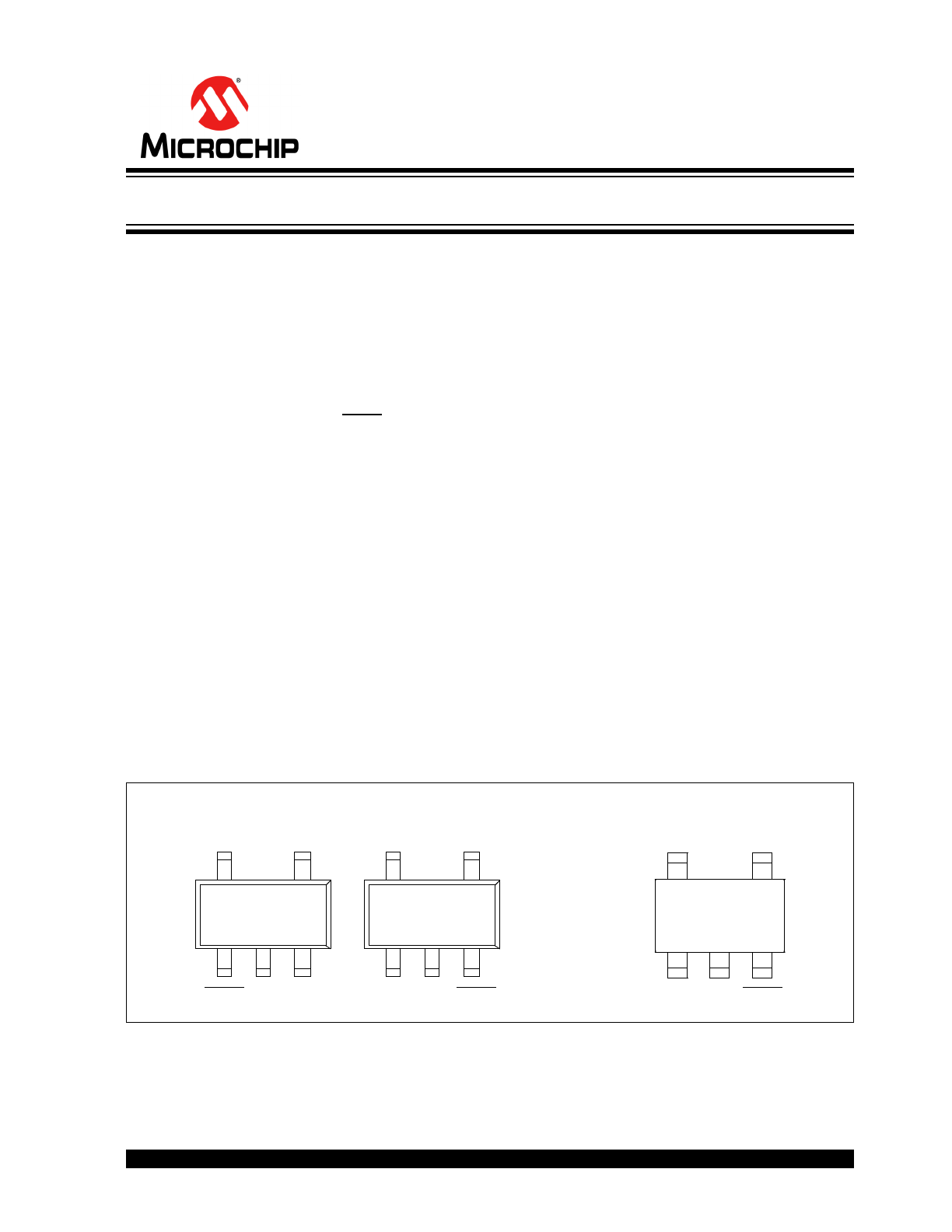
Package Types
SC-70
1
3
4
5
2
SHDN NC
V
OUT
V
IN
GND
TC1017
SOT-23
1
2
3
5
4
NC
V
OUT
SHDN
GND
V
IN
TC1017
1
3
4
5
2
V
IN
GND
NC
V
OUT
SHDN
TC1017R
150 mA, Tiny CMOS LDO With Shutdown
TC1017
DS21813F-page 2
2005-2013 Microchip Technology Inc.
1.0
ELECTRICAL
CHARACTERISTICS
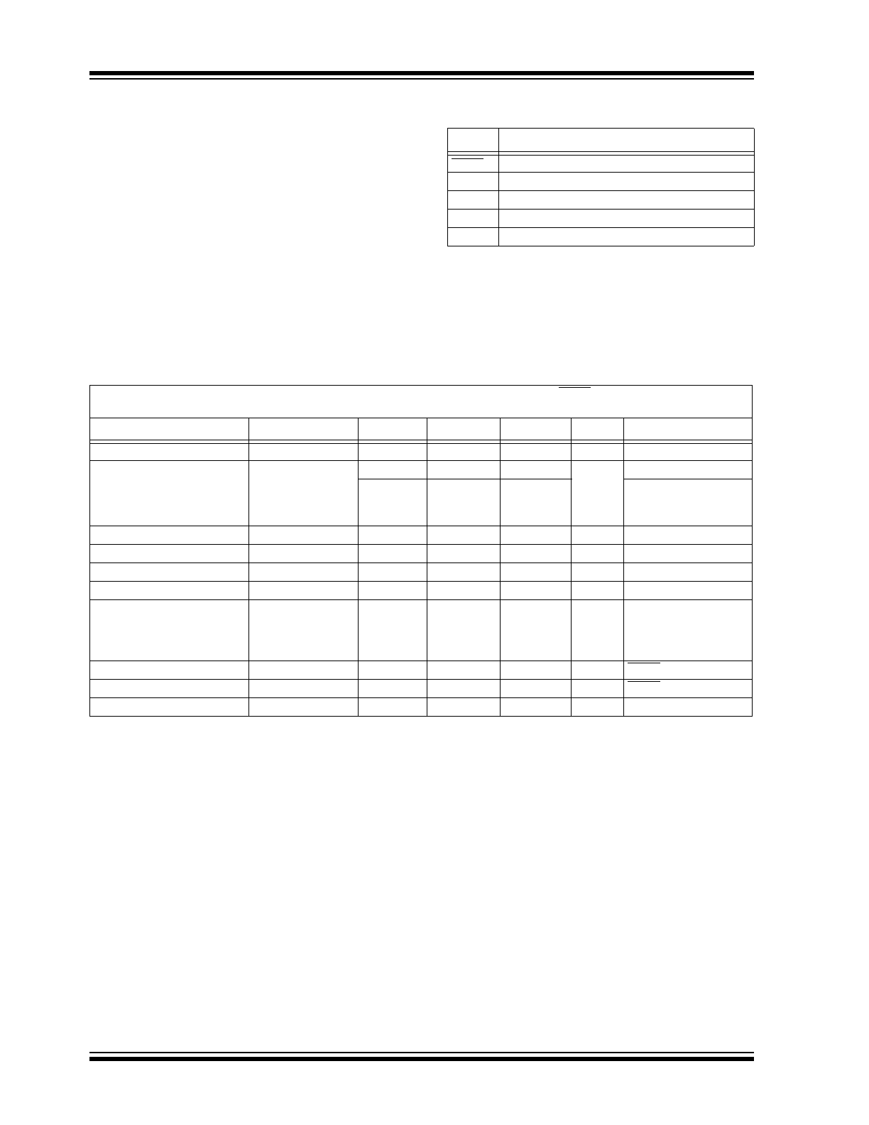
Absolute Maximum Ratings †
Input Voltage ....................................................................6.5V
Power Dissipation ......................... Internally Limited (Note 7)
Maximum Voltage On Any Pin ..................V
IN
+ 0.3V to -0.3V
† Notice: Stresses above those listed under “Maximum
Ratings” may cause permanent damage to the device. This is
a stress rating only and functional operation of the device at
those or any other conditions above those indicated in the
operation listings of this specification is not implied. Exposure
to maximum rating conditions for extended periods may affect
device reliability.
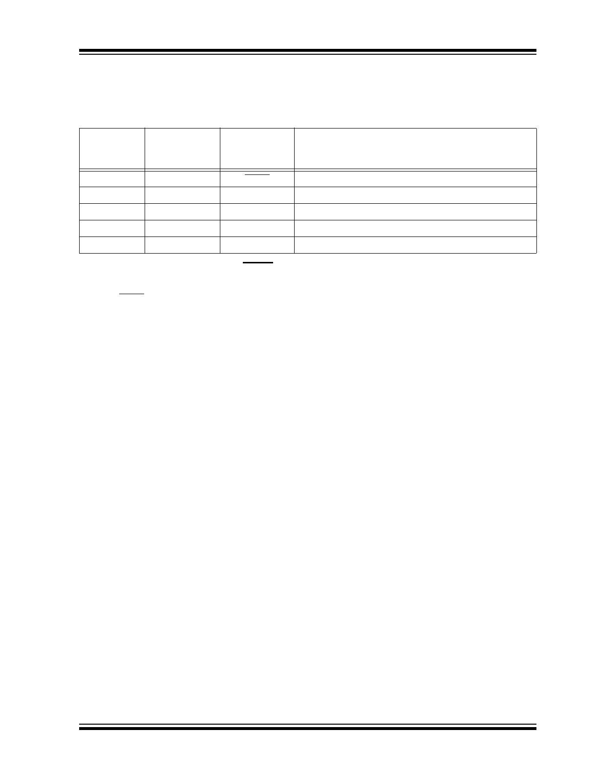
PIN FUNCTION TABLE
Name
Function
SHDN
Shutdown control input.
NC
No connect
GND
Ground terminal
V
OUT
Regulated voltage output
V
IN
Unregulated supply input
ELECTRICAL CHARACTERISTICS
Electrical Specifications: Unless otherwise noted, V
IN
= V
R
+ 1V, I
L
= 100 µA, C
L
= 1.0 µF, SHDN > V
IH
, T
A
= +25°C
Boldface type specifications apply for junction temperatures of –40°C to +125°C.
Parameter
Sym.
Min.
Typ.
Max.
Units
Test Conditions
Input Operating Voltage
V
IN
2.7
—
6.0
V
Note 1
Maximum Output Current
I
OUTMAX
100
—
—
mA
Note 1
150
—
—
V
IN
>= 3V and
V
IN
>= (V
R
+ 2.5%) +
V
DROPOUTMAX
Output Voltage
V
OUT
V
R
– 2.5%
V
R
±0.5%
V
R
+ 2.5%
V
Note 2
V
OUT
Temperature Coefficient
TCV
OUT
—
40
—
ppm/°C
Note 3
Line Regulation
V
OUT
/
V
IN
)| / V
R
—
0.04
0.2
%/V
(V
R
+ 1V) < V
IN
< 6V
Load Regulation (
Note 4
)
V
OUT
|
/ V
R
—
0.38
1.5
%
I
L
= 0.1 mA to I
OUTMAX
Dropout Voltage (
Note 5
)
V
IN
– V
OUT
—
—
—
—
2
90
180
285
—
200
350
500
mV
I
L
= 100 µA
I
L
= 50 mA
I
L
= 100 mA
I
L
= 150 mA
Supply Current
I
IN
—
53
90
µA
SHDN = V
IH
, I
L
= 0
Shutdown Supply Current
I
INSD
—
0.05
2
µA
SHDN = 0V
Power Supply Rejection Ratio
PSRR
—
58
—
dB
f =1 kHz, I
L
= 50 mA
Note 1:
The minimum V
IN
has to meet two conditions: V
IN
2.7V and V
IN
(V
R
+ 2.5%) + V
DROPOUT
.
2:
V
R
is the regulator voltage setting. For example: V
R
= 1.8V, 2.7V, 2.8V, 3.0V.
3:
4:
Regulation is measured at a constant junction temperature using low duty-cycle pulse testing. Load regulation is tested
over a load range from 0.1 mA to the maximum specified output current. Changes in output voltage due to heating
effects are covered by the thermal regulation specification.
5:
Dropout voltage is defined as the input-to-output differential at which the output voltage drops 2% below its nominal
value at a 1V differential.
6:
Thermal regulation is defined as the change in output voltage at a time T after a change in power dissipation is applied,
excluding load or line regulation effects. Specifications are for a current pulse equal to I
LMAX
at V
IN
= 6V for t = 10 msec.
7:
The maximum allowable power dissipation is a function of ambient temperature, the maximum allowable junction
temperature and the thermal resistance from junction-to-air (i.e., T
A
, T
J
,
JA
). Exceeding the maximum allowable power
dissipation causes the device to initiate thermal shutdown. Please see
Section 5.1 “Thermal Shutdown”
, for more
details
.
8:
Output current is limited to 120 mA (typ) when V
OUT
is less than 0.5V due to a load fault or short-circuit condition.
TCVOUT
VOUTMAX VOUTMIN
–
10
6
VOUT
T
--------------------------------------------------------------------------------------
=
2005-2013 Microchip Technology Inc.
DS21813F-page 3
TC1017
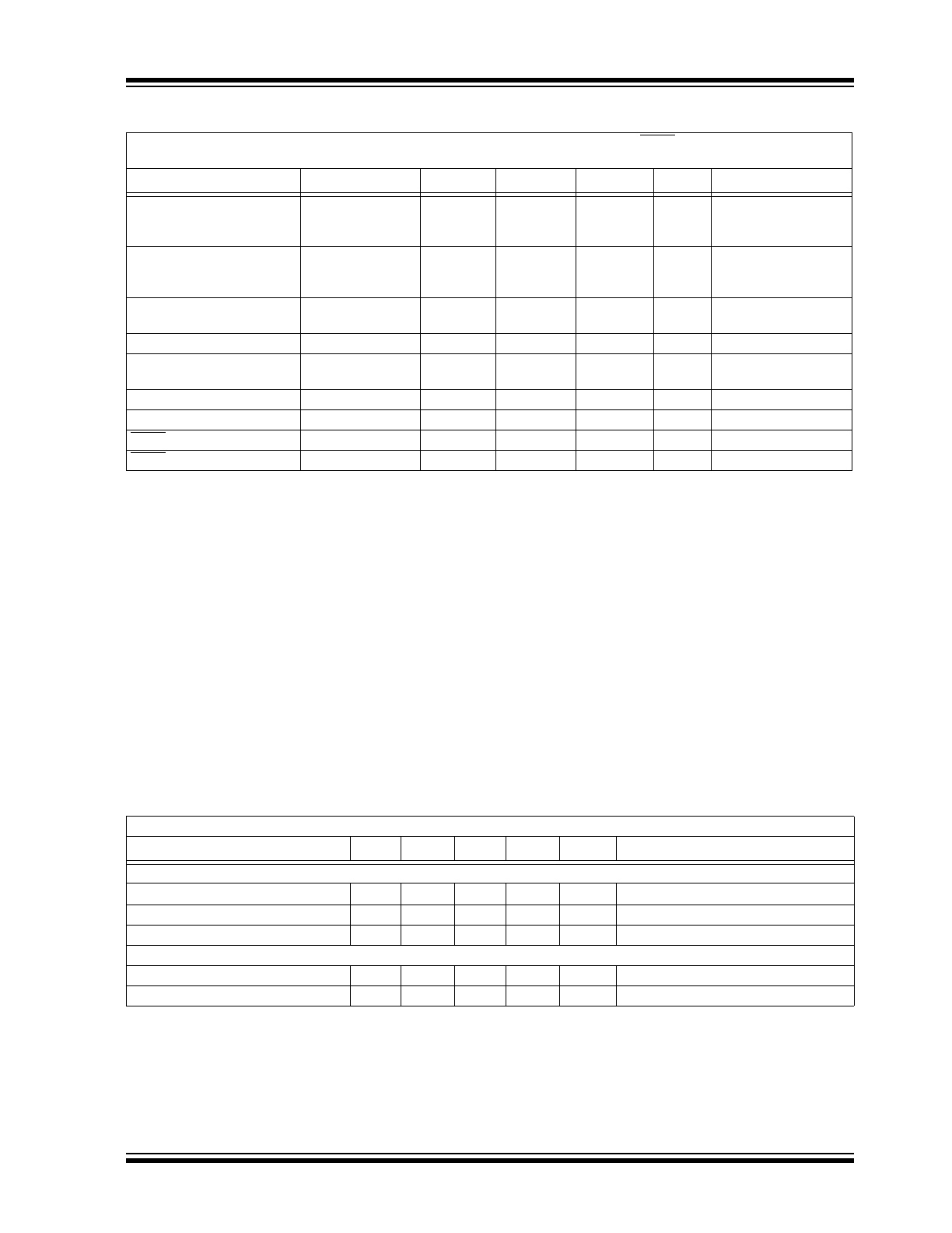
Wake-Up Time
(from Shutdown mode)
t
WK
—
10
—
µs
V
IN
= 5V, I
L
= 60 mA,
C
IN
= C
OUT
=1 µF,
f = 100 Hz
Settling Time
(from Shutdown mode)
t
S
—
32
—
µs
V
IN
= 5V, I
L
= 60 mA,
C
IN
= 1 µF,
C
OUT
= 1 µF, f = 100 Hz
Output Short-Circuit Current
I
OUTSC
—
120
—
mA
V
OUT
= 0V, Average
Current (
Note 8
)
Thermal Regulation
V
OUT
/P
D
—
0.04
—
V/W
Notes
6
,
7
Thermal Shutdown Die
Temperature
T
SD
—
160
—
°C
Thermal Shutdown Hysteresis
T
SD
—
10
—
°C
Output Noise
eN
—
800
—
nV/
Hz f = 10 kHz
SHDN Input High Threshold
V
IH
45
—
—
%V
IN
V
IN
= 2.7V to 6.0V
SHDN Input Low Threshold
V
IL
—
—
15
%V
IN
V
IN
= 2.7V to 6.0V
ELECTRICAL CHARACTERISTICS (CONTINUED)
Electrical Specifications: Unless otherwise noted, V
IN
= V
R
+ 1V, I
L
= 100 µA, C
L
= 1.0 µF, SHDN > V
IH
, T
A
= +25°C
Boldface type specifications apply for junction temperatures of –40°C to +125°C.
Parameter
Sym.
Min.
Typ.
Max.
Units
Test Conditions
Note 1:
The minimum V
IN
has to meet two conditions: V
IN
2.7V and V
IN
(V
R
+ 2.5%) + V
DROPOUT
.
2:
V
R
is the regulator voltage setting. For example: V
R
= 1.8V, 2.7V, 2.8V, 3.0V.
3:
4:
Regulation is measured at a constant junction temperature using low duty-cycle pulse testing. Load regulation is tested
over a load range from 0.1 mA to the maximum specified output current. Changes in output voltage due to heating
effects are covered by the thermal regulation specification.
5:
Dropout voltage is defined as the input-to-output differential at which the output voltage drops 2% below its nominal
value at a 1V differential.
6:
Thermal regulation is defined as the change in output voltage at a time T after a change in power dissipation is applied,
excluding load or line regulation effects. Specifications are for a current pulse equal to I
LMAX
at V
IN
= 6V for t = 10 msec.
7:
The maximum allowable power dissipation is a function of ambient temperature, the maximum allowable junction
temperature and the thermal resistance from junction-to-air (i.e., T
A
, T
J
,
JA
). Exceeding the maximum allowable power
dissipation causes the device to initiate thermal shutdown. Please see
Section 5.1 “Thermal Shutdown”
, for more
details
.
8:
Output current is limited to 120 mA (typ) when V
OUT
is less than 0.5V due to a load fault or short-circuit condition.
TCVOUT
VOUTMAX VOUTMIN
–
10
6
VOUT
T
--------------------------------------------------------------------------------------
=
TEMPERATURE CHARACTERISTICS
Electrical Specifications: Unless otherwise indicated, V
DD
= +2.7V to +6.0V and V
SS
= GND.
Parameters
Sym.
Min.
Typ.
Max.
Units
Conditions
Temperature Ranges
Specified Temperature Range
T
A
-40
—
+125
°C
Extended Temperature parts
Operating Temperature Range
T
A
-40
—
+125
°C
Storage Temperature Range
T
A
-65
—
+150
°C
Thermal Package Resistances3
Thermal Resistance, 5L-SOT23
JA
—
255
—
°C/W
Thermal Resistance, 5L-SC-70
JA
—
450
—
°C/W
TC1017
DS21813F-page 4
2005-2013 Microchip Technology Inc.
2.0
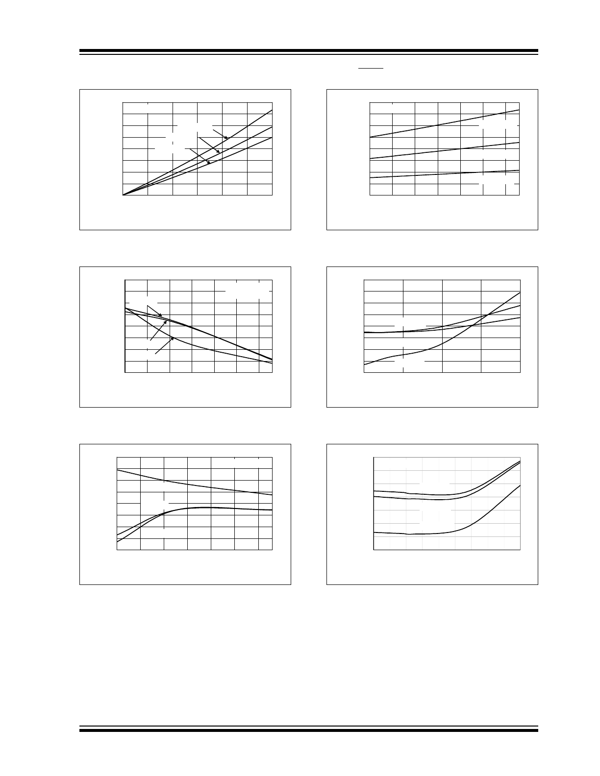
TYPICAL PERFORMANCE CHARACTERISTICS
Note: Unless otherwise noted, V
IN
= V
R
+ 1V, I
L
= 100 µA, C
L
= 1.0 µF, SHDN > V
IH
, T
A
= +25°C.
FIGURE 2-1:
Dropout Voltage vs. Output
Current.
FIGURE 2-2:
Load Regulation vs.
Temperature.
FIGURE 2-3:
Supply Current vs. Input
Voltage.
FIGURE 2-4:
Dropout Voltage vs.
Temperature.
FIGURE 2-5:
Short-Circuit Current vs.
Input Voltage.
FIGURE 2-6:
Supply Current vs.
Temperature.
Note:
The graphs and tables provided following this note are a statistical summary based on a limited number of
samples and are provided for informational purposes only. The performance characteristics listed herein
are not tested or guaranteed. In some graphs or tables, the data presented may be outside the specified
operating range (e.g., outside specified power supply range) and therefore outside the warranted range.
0.00
0.05
0.10
0.15
0.20
0.25
0.30
0.35
0.40
0
25
50
75
100
125
150
Load Current (mA)
D
ropout V
o
lt
age (V
)
T
A
= +125°C
T
A
= +25°C
T
A
= -40°C
V
OUT
= 2.85V
-0.70
-0.65
-0.60
-0.55
-0.50
-0.45
-0.40
-0.35
-0.30
-40
-15
10
35
60
85
110
Temperature (°C)
Load R
egul
ati
on (%
)
V
OUT
= 2.85V
I
OUT
= 0-150 mA
V
IN
= 6.0V
V
IN
= 3.85V
V
IN
= 3.3V
50
51
52
53
54
55
56
57
3.3
3.6
3.9
4.2
4.5
4.8
5.1
5.4
5.7
6.0
Input Voltage (V)
S
uppl
y C
u
rr
ent (µA
)
T
A
= -40°C
T
A
= +25°C
T
A
= +125°C
V
OUT
= 2.85V
0.00
0.05
0.10
0.15
0.20
0.25
0.30
0.35
0.40
-40
-15
10
35
60
85
110
Temperature (°C)
D
ropout V
o
lt
age (V
)
I
OUT
= 50 mA
I
OUT
= 100 mA
I
OUT
= 150 mA
V
OUT
= 2.85V
0
20
40
60
80
100
120
140
160
1
2
3
4
5
6
Input Voltage (V)
S
hor
t C
ir
cui
t C
u
rr
ent (m
A
)
V
OUT
= 2.85V
50
51
52
53
54
55
56
57
-40
-15
10
35
60
85
110
Temperature (°C)
S
uppl
y C
u
rr
ent (µA
)
V
IN
= 6.0V
V
IN
= 3.85V
V
IN
= 3.3V
V
OUT
= 2.85V
2005-2013 Microchip Technology Inc.
DS21813F-page 5
TC1017
Note: Unless otherwise noted, V
IN
= V
R
+ 1V, I
L
= 100 µA, C
L
= 1.0 µF, SHDN > V
IH
, T
A
= +25°C.
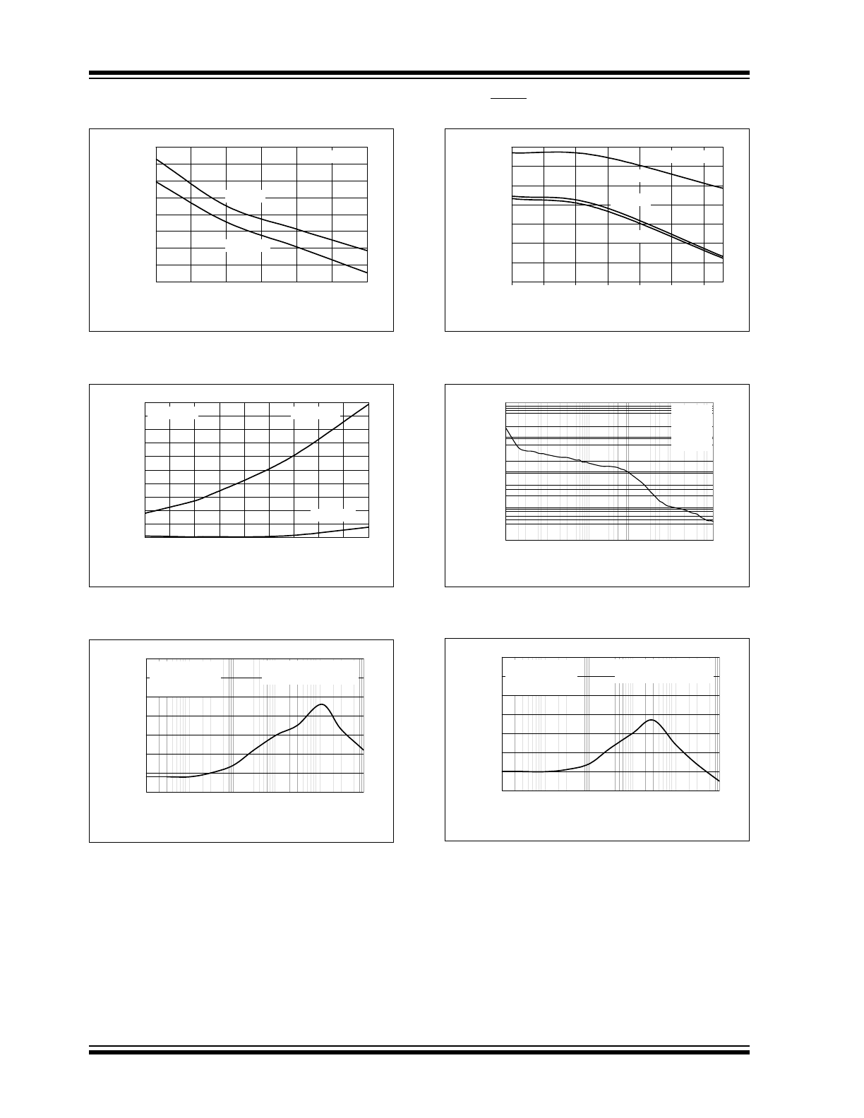
FIGURE 2-7:
Dropout Voltage vs. Output
Current.
FIGURE 2-8:
Load Regulation vs.
Temperature.
FIGURE 2-9:
Supply Current vs.
Temperature.
FIGURE 2-10:
Dropout Voltage vs.
Temperature.
FIGURE 2-11:
Supply Current vs. Input
Voltage.
FIGURE 2-12:
Output Voltage vs. Supply
Voltage.
0.00
0.05
0.10
0.15
0.20
0.25
0.30
0.35
0.40
0
25
50
75
100
125
150
Load Current (mA)
D
ropout V
o
lt
age (V
)
V
OUT
= 3.30V
T
A
= +125°C
T
A
= +25°C
T
A
= -40°C
-0.70
-0.65
-0.60
-0.55
-0.50
-0.45
-0.40
-0.35
-0.30
-40
-15
10
35
60
85
110
Temperature (°C)
Load R
egul
ati
on (%
)
V
OUT
= 3.30V
I
OUT
= 0-150 mA
V
IN
= 6.0V
V
IN
= 4.0V
V
IN
= 4.3V
52
53
54
55
56
57
58
59
60
-40
-15
10
35
60
85
110
Temperature (°C)
S
uppl
y C
u
rr
ent (µA
)
V
OUT
= 3.30V
V
IN
= 4.0V
V
IN
= 4.3V
V
IN
= 6.0V
0.00
0.05
0.10
0.15
0.20
0.25
0.30
0.35
0.40
-40
-15
10
35
60
85
110
Temperature (°C)
D
ropout V
o
lt
age (V
)
V
OUT
= 3.30V
I
OUT
= 150 mA
I
OUT
= 100 mA
I
OUT
= 50 mA
52
53
54
55
56
57
58
59
60
4.0
4.5
5.0
5.5
6.0
Input Voltage (V)
S
uppl
y C
u
rr
ent (µA
)
T
A
= +125°C
T
A
= +25°C
T
A
= -40°C
V
OUT
= 3.30V
2.862
2.863
2.864
2.865
2.866
2.867
2.868
2.869
3.3 3.6 3.9 4.2 4.5 4.8 5.1 5.4 5.7 6.0
Input Voltage (V)
Output V
o
ltage (V
)
V
OUT
= 2.85V
T
A
= -40°C
T
A
= +25°C
T
A
= +125°C
TC1017
DS21813F-page 6
2005-2013 Microchip Technology Inc.
Note: Unless otherwise noted, V
IN
= V
R
+ 1V, I
L
= 100 µA, C
L
= 1.0 µF, SHDN > V
IH
, T
A
= +25°C.
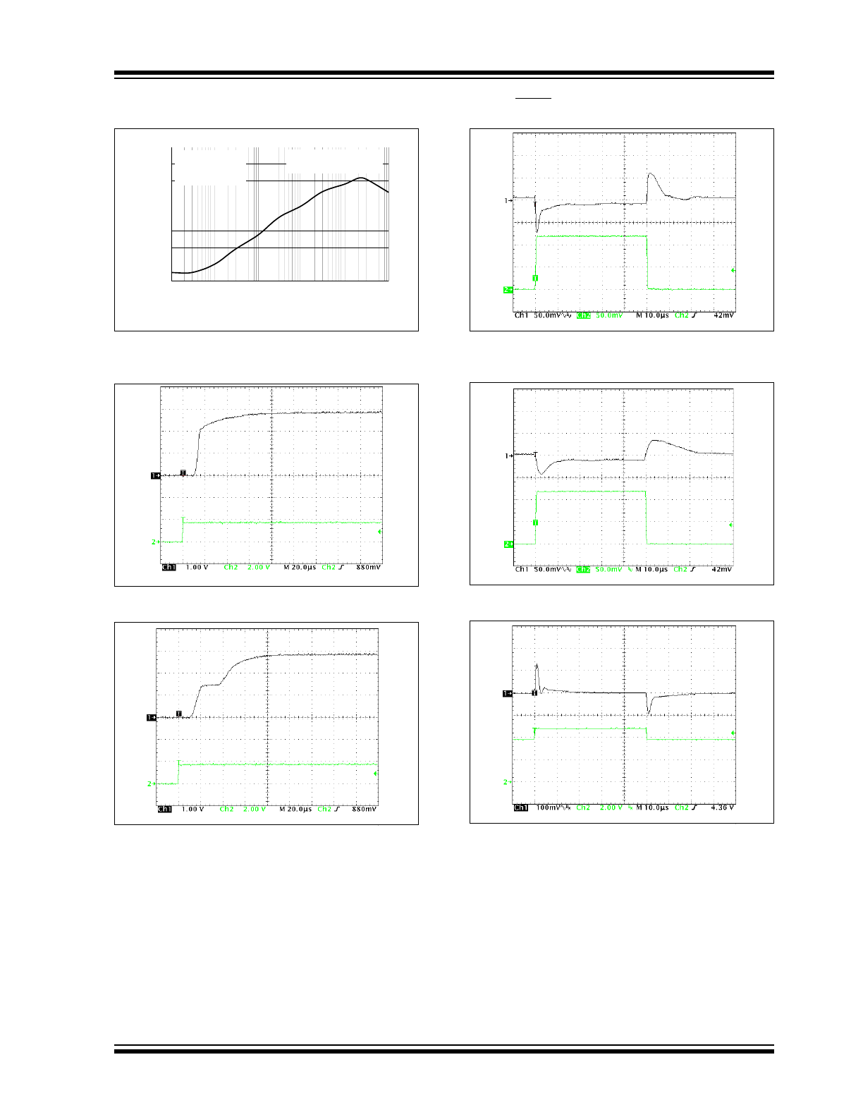
FIGURE 2-13:
Output Voltage vs. Output
Current.
FIGURE 2-14:
Shutdown Current vs. Input
Voltage.
FIGURE 2-15:
Power Supply Rejection
Ratio vs. Frequency.
FIGURE 2-16:
Output Voltage vs.
Temperature.
FIGURE 2-17:
Output Noise vs. Frequency.
FIGURE 2-18:
Power Supply Rejection
Ratio vs. Frequency.
2.854
2.856
2.858
2.860
2.862
2.864
2.866
2.868
2.870
0
25
50
75
100
125
150
Load Current (mA)
Output V
o
ltage (V
)
V
IN
= 3.85V
V
IN
= 6.0V
V
OUT
= 2.85V
0.0
0.2
0.4
0.6
0.8
1.0
1.2
1.4
1.6
1.8
2.0
3.3
3.6
3.9
4.2
4.5
4.8
5.1
5.4
5.7
6.0
Input Voltage (V)
S
hutdow
n C
u
rr
ent (µA
)
T
A
= +25°C
T
A
= +125°C
V
OUT
= 2.85V
-70
-60
-50
-40
-30
-20
-10
0
0.01
0.1
1
10
100
1000
Frequency (KHz)
PSRR
(dB)
V
INDC
= 3.85V
V
INAC
= 100 mVp-p
V
OUTDC
= 2.85V
I
OUT
= 100 μA
C
OUT
=1 μF X7R Ceramic
2.862
2.863
2.864
2.865
2.866
2.867
2.868
2.869
-40
-15
10
35
60
85
110
Temperature (°C)
Output V
o
ltage (V
)
V
IN
= 3.3V
V
IN
= 3.85V
V
IN
= 6.0V
V
OUT
= 2.85V
0.01
0.1
1
10
100
10
100
1000
10000
100000 1000000
Frequency (Hz)
Noise (µV/
Hz)
V
IN
= 3.85V
V
OUT
= 2.85V
C
IN
= 1 µF
C
OUT
= 1 µF
I
OUT
= 40 mA
-70
-60
-50
-40
-30
-20
-10
0
0.01
0.1
1
10
100
1000
Frequency (KHz)
PSRR
(dB)
V
INDC
= 3.85V
V
INAC
= 100 mVp-p
V
OUTDC
= 2.85V
I
OUT
= 1 mA
C
OUT
= 1 μF X7R Ceramic
2005-2013 Microchip Technology Inc.
DS21813F-page 7
TC1017
Note: Unless otherwise noted, V
IN
= V
R
+ 1V, I
L
= 100 µA, C
L
= 1.0 µF, SHDN > V
IH
, T
A
= +25°C.
FIGURE 2-19:
Power Supply Rejection
Ratio vs. Frequency.
FIGURE 2-20:
Wake-Up Response.
FIGURE 2-21:
Wake-Up Response.
FIGURE 2-22:
Load Transient Response.
FIGURE 2-23:
Load Transient Response.
FIGURE 2-24:
Line Transient Response.
-80
-70
-60
-50
-40
-30
-20
-10
0
0.01
0.1
1
10
100
1000
Frequency (KHz)
PSRR
(dB)
V
INDC
= 3.85V
V
INAC
= 100 mVp-p
V
OUTDC
= 2.85V
I
OUT
= 50 mA
C
OUT
= 1μF X7R Ceramic
V
IN
= 3.85V
C
IN
= 10 µF
C
OUT
= 1 µF Ceramic
Shutdow n Input
V
OUT
= 2.85V
V
IN
= 3.85V
C
IN
= 10 µF
C
OUT
= 4.7 µF Ceramic
Shutdow n Input
V
OUT
= 2.85V
V
IN
= 3.85V
C
IN
= 10 µF
C
OUT
= 1 µF Ceramic
V
OUT
= 2.85V
I
OUT
= 0.1 mA to 120 mA
V
IN
= 3.85V
C
IN
= 10 µF
C
OUT
= 4.7 µF Ceramic
V
OUT
= 2.85V
I
OUT
= 0.1 mA to 120 mA
C
IN
= 0 µF
C
OUT
= 1.0 µF Ceramic
I
LOAD
= 120 mA
V
OUT
= 2.85V
V
IN
= 3.85V to 4.85V
TC1017
DS21813F-page 8
2005-2013 Microchip Technology Inc.
Note: Unless otherwise noted, V
IN
= V
R
+ 1V, I
L
= 100 µA, C
L
= 1.0 µF, SHDN > V
IH
, T
A
= +25°C.
FIGURE 2-25:
Line Transient Response.
FIGURE 2-26:
Line Transient Response.
FIGURE 2-27:
Line Transient Response.
C
IN
= 0 µF
C
OUT
= 4.7 µF Ceramic
I
LOAD
= 120 mA
V
OUT
= 2.85V
V
IN
= 3.85V to 4.85V
C
IN
= 0 µF
C
OUT
= 1 µF Ceramic
I
LOAD
= 100 µA
V
OUT
= 3.33V
V
IN
= 4.3V to 5.3V
C
IN
= 0 µF
C
OUT
= 10 µF Ceramic
I
LOAD
= 100 µA
V
OUT
= 3.33V
V
IN
= 4.3V to 5.3V
2005-2013 Microchip Technology Inc.
DS21813F-page 9
TC1017
3.0
PIN DESCRIPTIONS
The descriptions of the pins are listed in
Table 3-1
.
TABLE 3-1:
PIN FUNCTION TABLE
3.1
Shutdown Control Input (SHDN)
The regulator is fully enabled when a logic-high is
applied to SHDN. The regulator enters shutdown when
a logic-low is applied to this input. During shutdown, the
output voltage falls to zero and the supply current is
reduced to 0.05 µA (typ.)
3.2
Ground Terminal
For best performance, it is recommended that the
ground pin be tied to a ground plane.
3.3
Regulated Voltage Output (V
OUT
)
Bypass the regulated voltage output to GND with a
minimum capacitance of 1 µF. A ceramic bypass
capacitor is recommended for best performance.
3.4
Unregulated Supply Input (V
IN
)
The minimum V
IN
has to meet two conditions in order
to ensure that the output maintains regulation:
V
IN
2.7V and V
IN
[(V
R
+ 2.5%) + V
DROPOUT
]. The
maximum V
IN
should be less than or equal to 6V.
Power dissipation may limit V
IN
to a lower potential in
order to maintain a junction temperature below 125°C.
Refer to
Section 5.0 “Thermal Considerations”
, for
determining junction temperature.
It is recommended that V
IN
be bypassed to GND with a
ceramic capacitor.
Pin No.
5-Pin SC-70
Pin No.
5-Pin SOT-23
5-Pin SC-70R
Symbol
Description
1
3
SHDN
Shutdown Control Input
2
4
NC
No Connect
3
2
GND
Ground Terminal
4
5
V
OUT
Regulated Voltage Output
5
1
V
IN
Unregulated Supply Input
TC1017
DS21813F-page 10
2005-2013 Microchip Technology Inc.
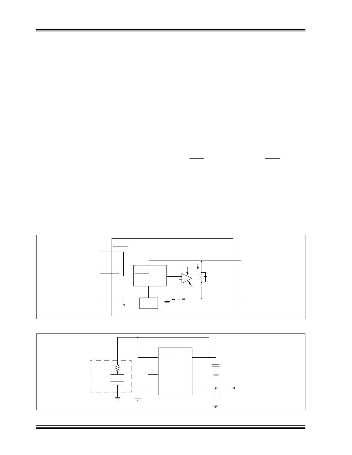
4.0
DETAILED DESCRIPTION
The TC1017 is a precision, fixed-output, linear voltage
regulator. The internal linear pass element is a
P-channel MOSFET. As with all P-channel CMOS
LDOs, there is a body drain diode with the cathode
connected to V
IN
and the anode connected to V
OUT
(
Figure 4-1
).
As is shown in
Figure 4-1
, the output voltage of the
LDO is sensed and divided down internally to reduce
external component count. The internal error amplifier
has a fixed bandgap reference on the inverting input
and the sensed output voltage on the non-inverting
input. The error amplifier output will pull the gate
voltage down until the inputs of the error amplifier are
equal to regulate the output voltage.
Output overload protection is implemented by sensing
the current in the P-channel MOSFET. During a shorted
or faulted load condition in which the output voltage
falls to less than 0.5V, the output current is limited to a
typical value of 120 mA. The current-limit protection
helps prevent excessive current from damaging the
Printed Circuit Board (PCB).
An internal thermal sensing device is used to monitor
the junction temperature of the LDO. When the sensed
temperature is over the set threshold of 160°C (typical),
the P-channel MOSFET is turned off. When the P-chan-
nel is off, the power dissipation internal to the device is
almost zero. The device cools until the junction tem-
perature is approximately 150°C and the P-channel is
turned on. If the internal power dissipation is still high
enough for the junction to rise to 160°C, it will again shut
off and cool. The maximum operating junction tempera-
ture of the device is 125°C. Steady-state operation at or
near the 160°C overtemperature point can lead to per-
manent damage of the device.
The output voltage V
OUT
remains stable over the entire
input operating voltage range (2.7V to 6.0V) and the
entire load range (0 mA to 150 mA). The output voltage
is sensed through an internal resistor divider and
compared with a precision internal voltage reference.
Several fixed-output voltages are available by
changing the value of the internal resistor divider.
Figure 4-2
shows a typical application circuit. The
regulator is enabled any time the shutdown input pin is
at or above V
IH
. It is shut down (disabled) any time the
shutdown input pin is below V
IL
. For applications where
the SHDN feature is not used, tie the SHDN pin directly
to the input supply voltage source. While in shutdown,
the supply current decreases to 0.006 µA (typical) and
the P-channel MOSFET is turned off.
As shown in
Figure 4-2
, batteries have internal source
impedance. An input capacitor is used to lower the
input impedance of the LDO. In some applications, high
input impedance can cause the LDO to become
unstable. Adding more input capacitance can
compensate for this.
FIGURE 4-1:
TC1017 Block Diagram (5-Pin SC-70 Pinout).
FIGURE 4-2:
Typical Application Circuit (5-Pin SC-70 Pinout).
+
-
EA
V
OUT
V
REF
SHDN
V
IN
5
4
R
1
R
2
1
2
3
SHDN
GND
V
IN
NC
Current Limit
Over
Error
Feedback Resistors
Control
Temp.
Body
Diode
Amp
V
OUT
5
4
1
2
3
SHDN
GND
V
IN
NC
BA
TTER
Y R
SOURCE
C
IN
1 µF Ceramic
C
OUT
1 µF Ceramic
TC1017
Load