
© 2009 Microchip Technology Inc.
DS22005B-page 1
MCP73833/4
Features
• Complete Linear Charge Management Controller
- Integrated Pass Transistor
- Integrated Current Sense
- Integrated Reverse Discharge Protection
• Constant Current / Constant Voltage Operation
with Thermal Regulation
• High Accuracy Preset Voltage Regulation:
- 4.2V, 4.35V, 4.4V, or 4.5V, + 0.75%
• Programmable Charge Current: 1A Maximum
• Preconditioning of Deeply Depleted Cells
- Selectable Current Ratio
- Selectable Voltage Threshold
• Automatic End-of-Charge Control
- Selectable Current Threshold
- Selectable Safety Time Period
• Automatic Recharge
- Selectable Voltage Threshold
• Two Charge Status Outputs
• Cell Temperature Monitor
• Low-Dropout Linear Regulator Mode
• Automatic Power-Down when Input Power
Removed
• Under Voltage Lockout
• Numerous Selectable Options Available for a
Variety of Applications:
- Refer to Section 1.0 “Electrical
Characteristics” for Selectable Options
- Refer to the Product Identification System for
Standard Options
• Available Packages:
- DFN-10 (3 mm x 3 mm)
- MSOP-10
Applications
• Lithium-Ion / Lithium-Polymer Battery Chargers
• Personal Data Assistants
• Cellular Telephones
• Digital Cameras
• MP3 Players
• Bluetooth Headsets
• USB Chargers
Description
The MCP73833/4 is a highly advanced linear charge
management controller for use in space-limited, cost
sensitive applications. The MCP73833/4 is available in
a 10-Lead, 3 mm x 3 mm DFN package or a 10-Lead,
MSOP package. Along with its small physical size, the
low number of external components required makes
the MCP73833/4 ideally suited for portable
applications. For applications charging from a USB
port, the MCP73833/4 can adhere to all the
specifications governing the USB power bus.
The MCP73833/4 employs a constant current/constant
voltage charge algorithm with selectable precondition-
ing and charge termination. The constant voltage
regulation is fixed with four available options: 4.20V,
4.35V, 4.40V, or 4.50V, to accomodate new, emerging
battery charging requirements. The constant current
value is set with one external resistor. The MCP73833/
4 limits the charge current based on die temperature
during high power or high ambient conditions. This
thermal regulation optimizes the charge cycle time
while maintaining device reliability.
Several options are available for the preconditioning
threshold, preconditioning current value, charge
termination value, and automatic recharge threshold.
The preconditioning value and charge termination
value are set as a ratio, or percentage, of the
programmed constant current value. Preconditioning
can be set
to 100%
. Refer to Section 1.0 “Electrical
Characteristics” for available options and the
“Product Indentification System” for standard
options.
The MCP73833/4 is fully specified over the ambient
temperature range of -40°C to +85°C.
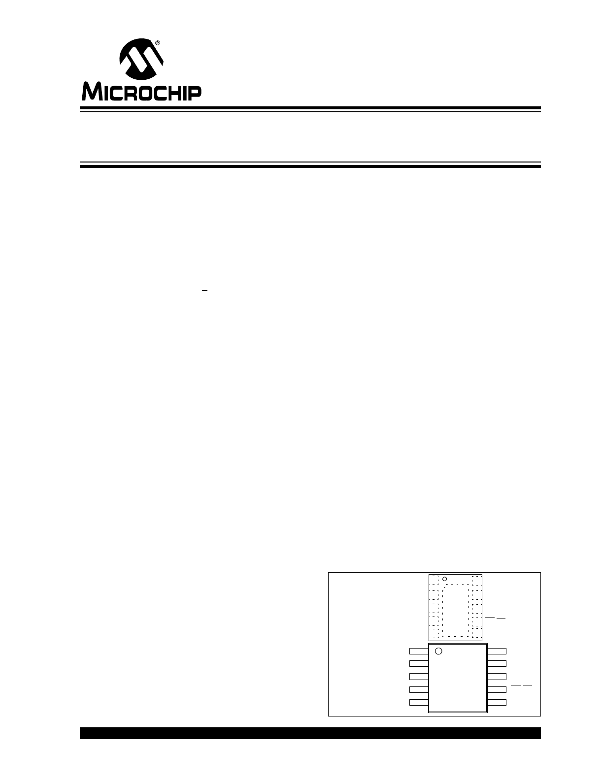
Package Types
DFN-10
MSOP-10
V
DD
STAT1
STAT2
V
SS
V
BAT
THERM
PG(TE)
PROG
2
3
4
5
9
8
7
6
V
DD
V
BAT
1
10
STAT1
V
DD
STAT2
V
BAT
THERM
1
2
3
4
10
9
8
7
PG(TE)
V
BAT
V
DD
EP
11
5
6
PROG
V
SS
Stand-Alone Linear Li-Ion / Li-Polymer Charge
Management Controller
MCP73833/4
DS22005B-page 2
© 2009 Microchip Technology Inc.
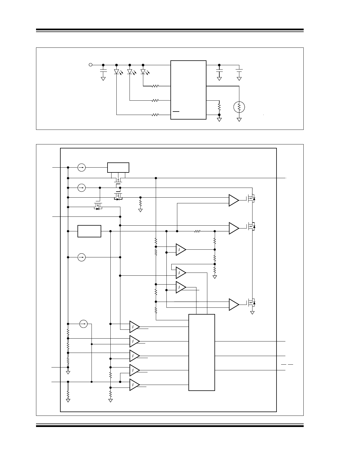
Typical Application
Functional Block Diagram
STAT1
V
DD
V
SS
PROG
V
BAT
+
-
Single
Li-Ion
Cell
1,2
MCP73833
6
9,10
7
1 µF
1A Li-Ion Battery Charger
5
V
IN
470
Ω
470
Ω
470
Ω
STAT2
PG
THERM
T
4
3
8
1 µF
1 k
Ω
10 k
Ω
+
-
Reference
Generator
V
REF
(1.21V)
V
DD
STAT1
PROG
V
BAT
G=0.001
V
SS
Direction
Control
54 k
Ω
121 k
Ω
UVLO
+
-
PRECONDITION
6 µA
+
-
TERMINATIO N
+
-
111 k
Ω
+
-
CA
10 k
Ω
157.3 k
Ω
6 k
Ω
48 k
Ω
470.6 k
Ω
CHARG E
+
-
+
-
VA
72.7 k
Ω
310 k
Ω
6 µA
G=0.001
1 k
Ω
+
-
CURRENT
LIMIT
10 µA
+
-
LTVT
+
-
HTVT
470.6k
Ω
121 k
Ω
THERM
50 µA
Charge
Control,
Timer,
and
Status
Logic
STAT2
PG (TE)
+
-
LDO
1 M
Ω
175 k
Ω
SHDN
© 2009 Microchip Technology Inc.
DS22005B-page 3
MCP73833/4
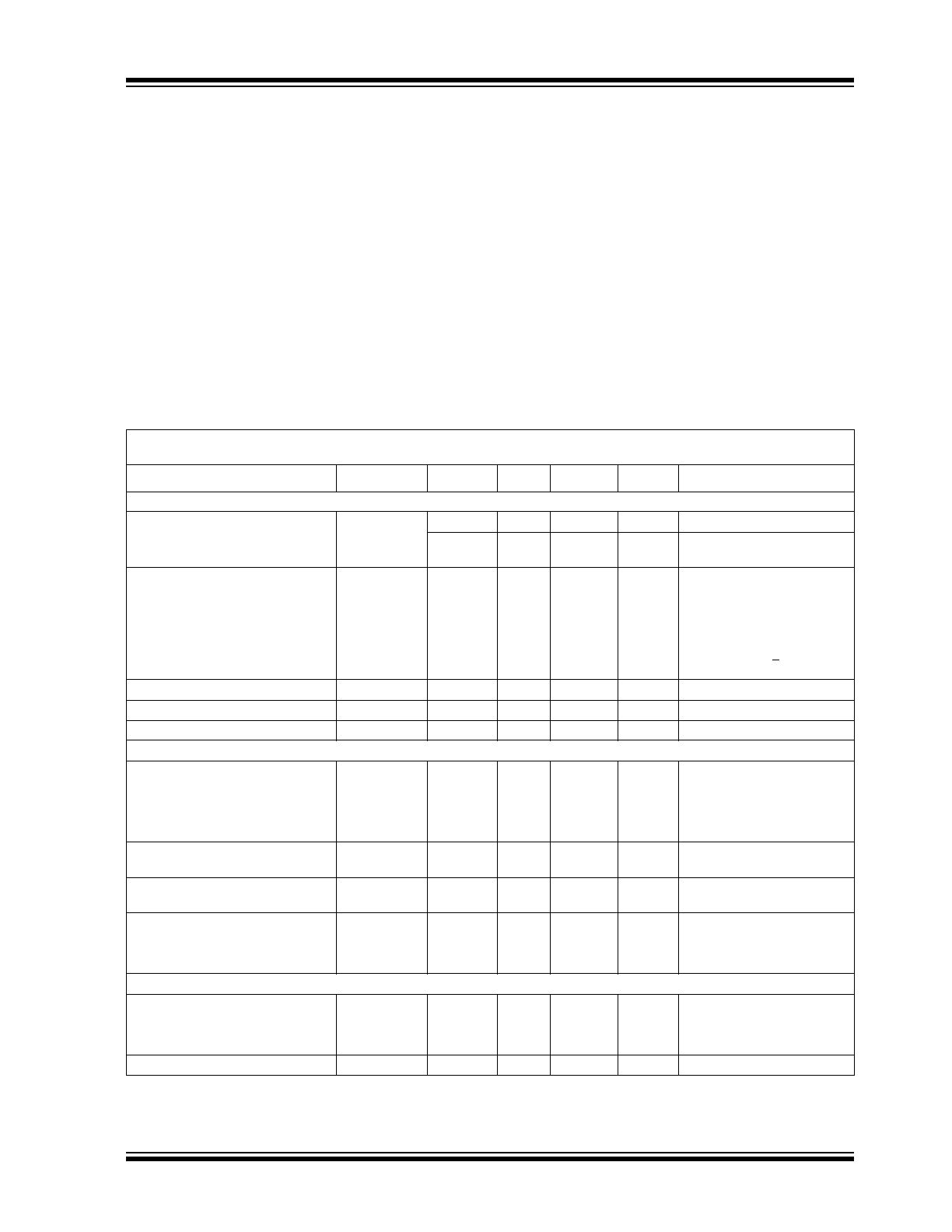
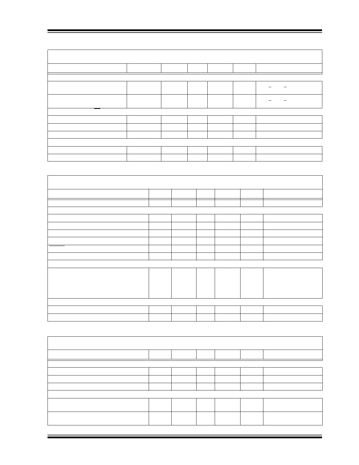
1.0
ELECTRICAL
CHARACTERISTICS
Absolute Maximum Ratings
V
DD
........................................................................ 7.0V
All Inputs and Outputs w.r.t. V
SS
.....-0.3 to (V
DD
+0.3)V
Maximum Junction Temperature, T
J
. Internally Limited
Storage temperature .......................... -65°C to +150°C
ESD protection on all pins:
Human Body Model (HBM)
(1.5 k
Ω in Series with 100 pF)............................... ≥ 4 kV
Machine Model (MM)
(200 pF, No Series Resistance) ........................... 300V
*Notice: Stresses above those listed under “Maximum
Ratings” may cause permanent damage to the device.
This is a stress rating only and functional operation of
the device at those or any other conditions above those
indicated in the operational listings of this specification
is not implied. Exposure to maximum rating conditions
for extended periods may affect device reliability.
DC CHARACTERISTICS
Electrical Specifications: Unless otherwise specified, all limits apply for V
DD
= [V
REG
(Typical)+0.3V] to 6V, T
A
=-40°C to 85°C.
Typical values are at +25°C, V
DD
= [V
REG
(Typical)+1.0V]
Parameters
Sym
Min
Typ
Max
Units
Conditions
Supply Input
Supply Voltage
V
DD
3.75
—
6
V
Charging
V
REG
(Typ-
ical)+0.3V
—
6
V
Charge Complete, Standby
Supply Current
I
SS
—
2000
3000
µA
Charging
—
150
300
µA
Charge Complete
—
100
300
µA
Standby (No Battery or PROG
Floating)
—
50
100
µA
Shutdown (V
DD
< V
BAT
, or
V
DD
< V
STOP
)
UVLO Start Threshold
V
START
3.4
3.55
3.7
V
V
DD
Low-to-High
UVLO Stop Threshold
V
STOP
3.3
3.45
3.6
V
V
DD
High-to-Low
UVLO Hysteresis
V
HYS
—
100
—
mV
Voltage Regulation (Constant Voltage Mode, System Test Mode)
Regulated Output Voltage
V
REG
4.168
4.20
4.232
V
V
DD
=[V
REG
(Typical)+1V]
4.318
4.35
4.382
V
I
OUT
=10 mA
4.367
4.40
4.433
V
T
A
=-5°C to +55°C
4.467
4.50
4.533
V
Line Regulation
|(ΔV
BAT
/V
BAT
)
/
ΔV
DD
|
—
0.10
0.30
%/V
V
DD
=[V
REG
(Typical)+1V] to
6V, I
OUT
=10 mA
Load Regulation
|ΔV
BAT
/ V
BAT
|
—
0.10
0.30
%
I
OUT
=10 mA to 100 mA
V
DD
=[V
REG
(Typical)+1V]
Supply Ripple Attenuation
PSRR
—
58
—
dB
I
OUT
=10 mA, 10Hz to 1 kHz
—
47
—
dB
I
OUT
=10 mA, 10Hz to 10 kHz
—
25
—
dB
I
OUT
=10 mA, 10Hz to 1 MHz
Current Regulation (Fast Charge Constant Current Mode)
Fast Charge Current Regulation
I
REG
90
100
110
mA
PROG = 10 k
Ω
900
1000
1100
mA
PROG = 1.0 k
Ω
T
A
=-5°C to +55°C
Maximum Output Current Limit
I
MAX
—
1200
—
mA
PROG < 833
Ω
MCP73833/4
DS22005B-page 4
© 2009 Microchip Technology Inc.
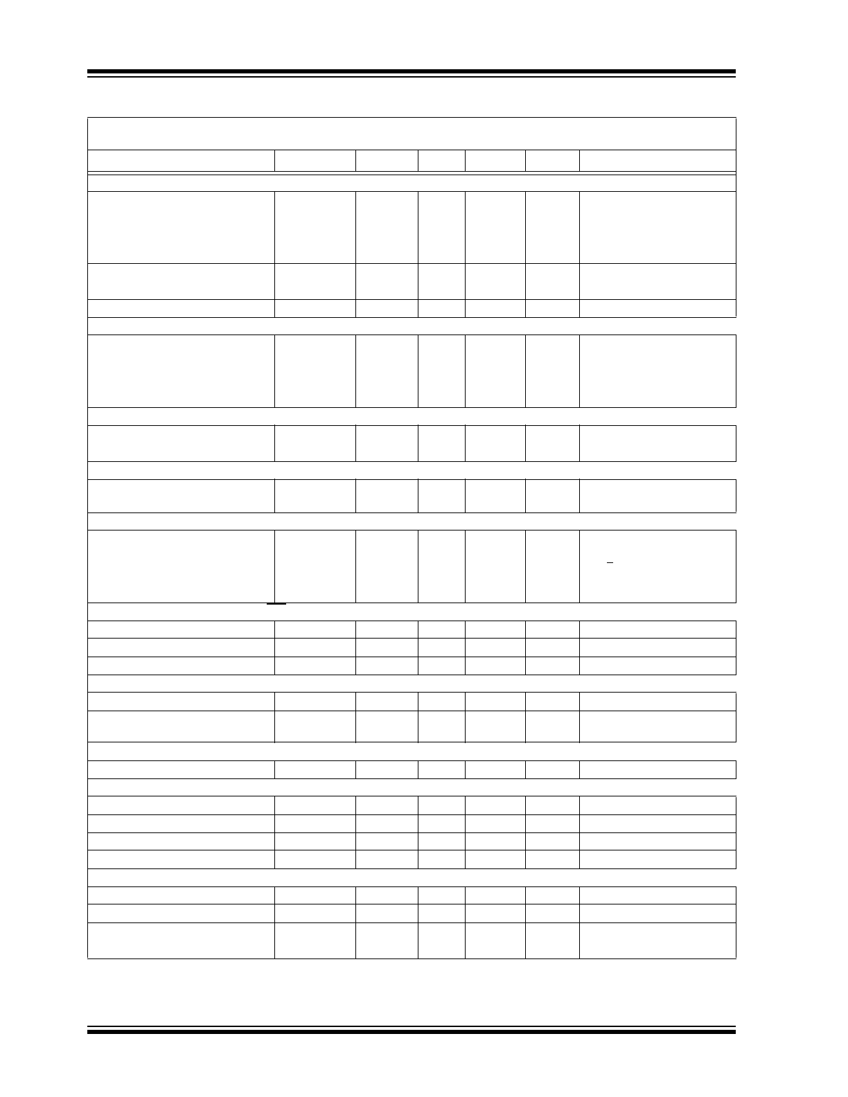
Preconditioning Current Regulation (Trickle Charge Constant Current Mode)
Precondition Current Ratio
I
PREG
/ I
REG
7.5
10
12.5
%
PROG = 1.0 k
Ω to 10 kΩ
15
20
25
%
T
A
=-5°C to +55°C
30
40
50
%
—
100
—
%
Precondition Voltage Threshold
Ratio
V
PTH
/ V
REG
64
66.5
70
%
V
BAT
Low-to-High
69
71.5
75
%
Precondition Hysteresis
V
PHYS
—
100
—
mV
V
BAT
High-to-Low
Charge Termination
Charge Termination Current Ratio
I
TERM
/ I
REG
3.75
5
6.25
%
PROG = 1.0 k
Ω to 10 kΩ
5.6
7.5
9.4
%
T
A
=-5°C to +55°C
7.5
10
12.5
%
15
20
25
%
Automatic Recharge
Recharge Voltage Threshold Ratio
V
RTH
/ V
REG
—
94.0
—
%
V
BAT
High-to-Low
—
96.5
—
%
Pass Transistor ON-Resistance
ON-Resistance
R
DSON
—
300
—
m
Ω
V
DD
= 3.75V
T
J
= 105°C
Battery Discharge Current
Output Reverse Leakage Current
I
DISCHARGE
—
0.15
2
µA
PROG Floating
—
0.25
2
µA
V
DD
< V
BAT
—
0.15
2
µA
V
DD
< V
STOP
—
-5.5
-15
µA
Charge Complete
Status Indicators - STAT1, STAT2, PG
Sink Current
I
SINK
—
15
25
mA
Low Output Voltage
V
OL
—
0.4
1
V
I
SINK
= 4 mA
Input Leakage Current
I
LK
—
0.01
1
µA
High Impedance, 6V on pin
PROG Input
Charge Impedance Range
R
PROG
1
—
20
k
Ω
Standy Impedance
R
PROG
70
—
200
k
Ω
Minimum Impedance for
Standby
Thermistor Bias
Thermistor Current Source
I
THERM
47
50
53
µA
2 k
Ω < R
THERM
< 50 k
Ω
Thermistor Comparator
Upper Trip Threshold
V
T1
1.20
1.23
1.26
V
V
THERM
Low-to-High
Upper Trip Point Hysteresis
V
T1HYS
—
-50
—
mV
Lower Trip Threshold
V
T2
0.235
0.25
0.265
V
V
THERM
High-to-Low
Lower Trip Point Hysteresis
V
T2HYS
—
50
—
mV
System Test (LDO) Mode
Input High Voltage Level
V
IH
(V
DD
-0.1)
—
—
V
THERM Input Sink Current
I
SINK
3
6
20
µA
Stand-by or system test mode
Bypass Capacitance
C
BAT
1
—
—
µF
I
OUT
< 250 mA
4.7
—
—
µF
I
OUT
> 250 mA
DC CHARACTERISTICS (CONTINUED)
Electrical Specifications: Unless otherwise specified, all limits apply for V
DD
= [V
REG
(Typical)+0.3V] to 6V, T
A
=-40°C to 85°C.
Typical values are at +25°C, V
DD
= [V
REG
(Typical)+1.0V]
Parameters
Sym
Min
Typ
Max
Units
Conditions
© 2009 Microchip Technology Inc.
DS22005B-page 5
MCP73833/4
TEMPERATURE SPECIFICATIONS
Automatic Power Down
Automatic Power Down Entry
Threshold
V
PD
—
V
BAT
+
50 mV
—
V
2.3V < V
BAT
< V
REG
V
DD
Falling
Automatic Power Down Exit Thresh-
old
V
PDEXIT
—
V
BAT
+
150 mV
—
V
2.3V < V
BAT
< V
REG
V
DD
Rising
Timer Enable Input (TE)
Input High Voltage Level
V
IH
2.0
—
—
V
Input Low Voltage Level
V
IL
—
—
0.6
V
Input Leakage Current
I
LK
—
0.01
1
µA
V
TE
= 6V
Thermal Shutdown
Die Temperature
T
SD
—
150
—
°C
Die Temperature Hysteresis
T
SDHYS
—
10
—
°C
DC CHARACTERISTICS (CONTINUED)
Electrical Specifications: Unless otherwise specified, all limits apply for V
DD
= [V
REG
(Typical)+0.3V] to 6V, T
A
=-40°C to 85°C.
Typical values are at +25°C, V
DD
= [V
REG
(Typical)+1.0V]
Parameters
Sym
Min
Typ
Max
Units
Conditions
AC CHARACTERISTICS
Electrical Specifications: Unless otherwise specified, all limits apply for V
DD
= [V
REG
(Typical)+0.3V] to 6V, T
A
=-40°C to 85°C.
Typical values are at +25°C, V
DD
= [V
REG
(Typical)+1.0V]
Parameters
Sym
Min
Typ
Max
Units
Conditions
UVLO Start Delay
t
START
—
—
5
ms
V
DD
Low-to-High
Current Regulation
Transition Time Out of Preconditioning
t
DELAY
—
—
1
ms
V
BAT
<V
PTH
to V
BAT
>V
PTH
Current Rise Time Out of Preconditioning
t
RISE
—
—
1
ms
I
OUT
Rising to 90% of I
REG
Preconditioning Comparator Filter Time
t
PRECON
0.4
1.3
3.2
ms
Average V
BAT
Rise/Fall
Termination Comparator Filter Time
t
TERM
0.4
1.3
3.2
ms
Average I
OUT
Falling
Charge Comparator Filter Time
t
CHARGE
0.4
1.3
3.2
ms
Average V
BAT
Falling
Thermistor Comparator Filter Time
t
THERM
0.4
1.3
3.2
ms
Average THERM Rise/Fall
Elapsed Timer
Elapsed Timer Period
t
ELAPSED
0
0
0
Hours
Timer Disabled
3.6
4.0
4.4
Hours
5.4
6.0
6.6
Hours
7.2
8.0
8.8
Hours
Status Indicators
Status Output turn-off
t
OFF
—
—
200
µs
I
SINK
= 1 mA to 0 mA
Status Output turn-on
t
ON
—
—
200
µs
I
SINK
= 0 mA to 1 mA
Electrical Specifications: Unless otherwise specified, all limits apply for V
DD
= [V
REG
(Typical)+0.3V] to 6V.
Typical values are at +25°C, V
DD
= [V
REG
(Typical)+1.0V]
Parameters
Symbol
Min
Typ
Max
Units
Conditions
Temperature Ranges
Specified Temperature Range
T
A
-40
—
+85
°C
Operating Temperature Range
T
A
-40
—
+125
°C
Storage Temperature Range
T
A
-65
—
+150
°C
Thermal Package Resistances
Thermal Resistance, MSOP-10
θ
JA
—
113
—
°C/W
4-Layer JC51-7 Standard
Board, Natural Convection
Thermal Resistance, DFN-10, 3 mm x 3 mm
θ
JA
—
41
—
°C/W
4-Layer JC51-7 Standard
Board, Natural Convection

MCP73833/4
DS22005B-page 6
© 2009 Microchip Technology Inc.
NOTES:
© 2009 Microchip Technology Inc.
DS22005B-page 7
MCP73833/4
2.0
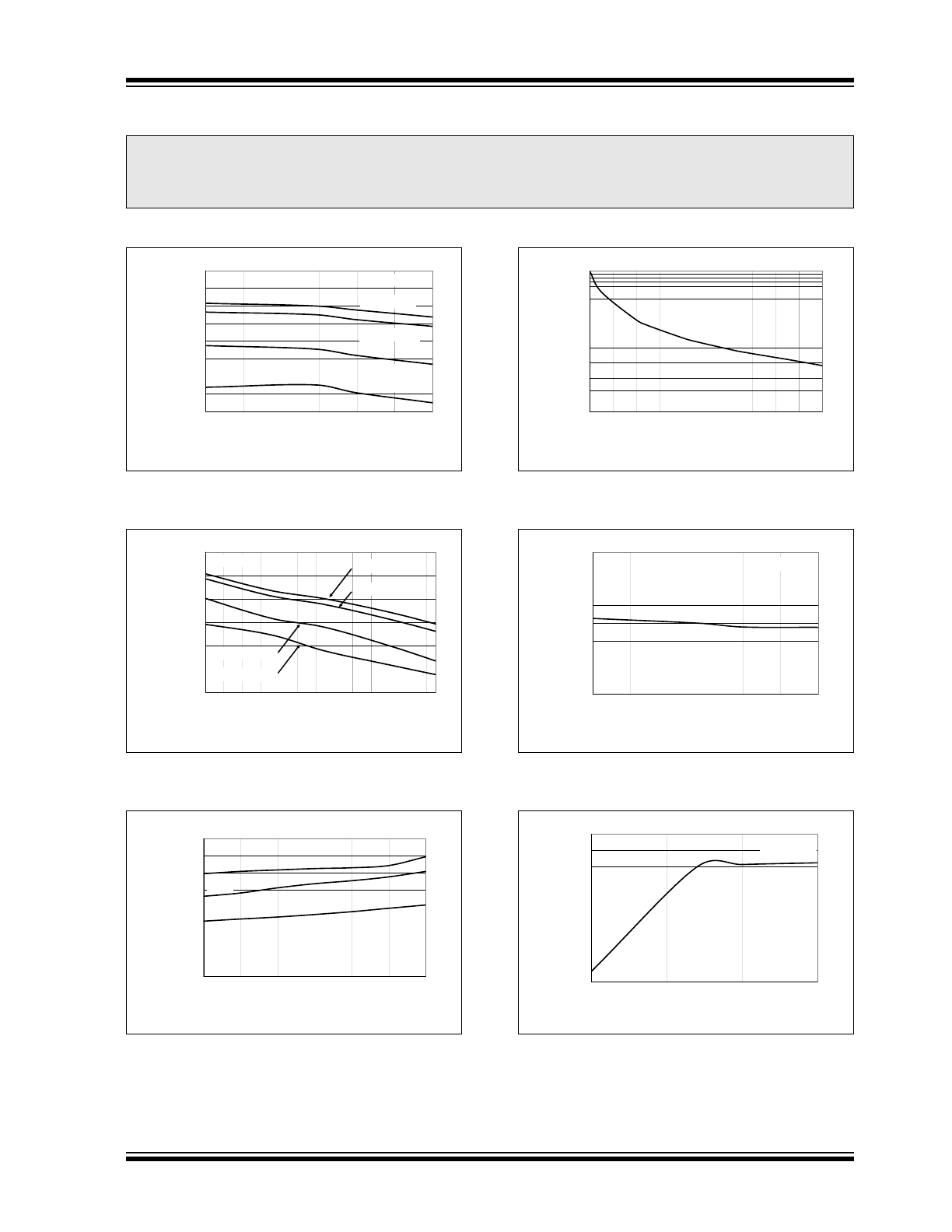
TYPICAL PERFORMANCE CURVES
Note: Unless otherwise indicated, V
DD
= 5.2V, V
REG
= 4.20V, I
OUT
= 10 mA and T
A
= +25°C, Constant-voltage mode.
FIGURE 2-1:
Battery Regulation Voltage
(V
BAT
) vs. Supply Voltage (V
DD
).
FIGURE 2-2:
Battery Regulation Voltage
(V
BAT
) vs. Ambient Temperature (T
A
).
FIGURE 2-3:
Output Leakage Current
(I
DISCHARGE
) vs. Battery Regulation Voltage
(V
BAT
).
FIGURE 2-4:
Charge Current (I
OUT
) vs.
Programming Resistor (R
PROG
).
FIGURE 2-5:
Charge Current (I
OUT
) vs.
Supply Voltage (V
DD
).
FIGURE 2-6:
Charge Current (I
OUT
) vs.
Supply Voltage (V
DD
).
Note:
The graphs and tables provided following this note are a statistical summary based on a limited number of
samples and are provided for informational purposes only. The performance characteristics listed herein
are not tested or guaranteed. In some graphs or tables, the data presented may be outside the specified
operating range (e.g., outside specified power supply range) and therefore outside the warranted range.
4.170
4.175
4.180
4.185
4.190
4.195
4.200
4.205
4.210
4.50
4.75
5.00
5.25
5.50
5.75
6.00
Supply Voltage (V)
B
attery
R
e
g
u
la
ti
on
V
o
lta
g
e
(V
)
MCP73833
I
OUT
= 10 mA
I
OUT
= 100 mA
I
OUT
= 500 mA
I
OUT
= 900 mA
4.160
4.170
4.180
4.190
4.200
4.210
4.220
-40
-30
-20
-10
0
10
20
30
40
50
60
70
80
Ambient Temperature (°C)
Battery R
egu
la
ti
on
V
o
lt
a
g
e
(V
)
MCP73833
I
OUT
= 10 mA
I
OUT
= 100 mA
I
OUT
= 500 mA
I
OUT
= 900 mA
0.00
0.05
0.10
0.15
0.20
0.25
0.30
0.35
0.40
3.00
3.20
3.40
3.60
3.80
4.00
4.20
Battery Regulation Voltage (V)
Output Leakage Current (
P
A)
+85°C
-40°C
+25°C
10
100
1000
1
3
5
7
9
11 13 15 17 19 21
Programming Resistor (k:)
Charge Current (mA)
96
97
98
99
100
101
102
103
104
4.50
4.75
5.00
5.25
5.50
5.75
6.00
Supply Voltage (V)
Charge Current (mA)
R
PROG
= 10 k:
986
988
990
992
994
996
998
1000
1002
1004
4.50
4.75
5.00
5.25
5.50
5.75
6.00
Supply Voltage (V)
Charge Current (mA)
R
PROG
= 1 k:
MCP73833/4
DS22005B-page 8
© 2009 Microchip Technology Inc.
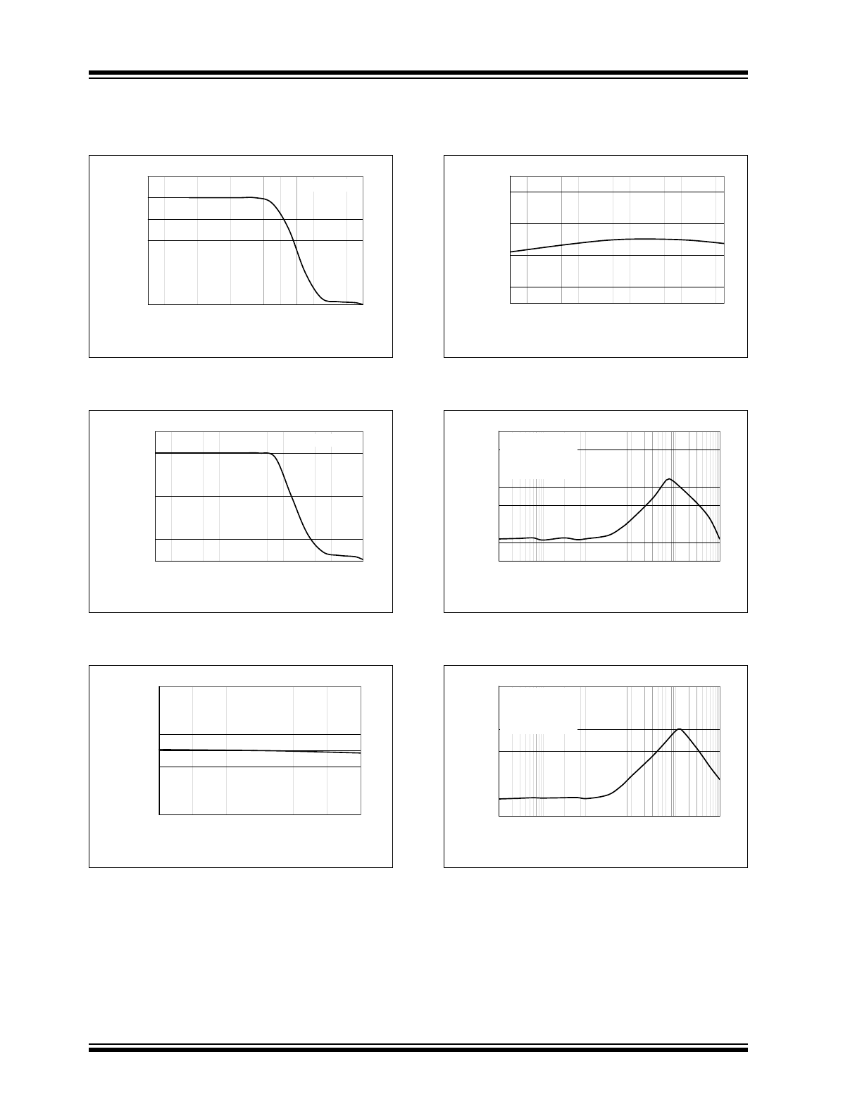
TYPICAL PERFORMANCE CURVES
(Continued)
Note: Unless otherwise indicated, V
DD
= 5.2V, V
REG
= 4.20V, I
OUT
= 10 mA and T
A
= +25°C, Constant-voltage mode.
FIGURE 2-7:
Charge Current (I
OUT
) vs.
Junction Temperature (T
J
).
FIGURE 2-8:
Charge Current (I
OUT
) vs.
Junction Temperature (T
J
).
FIGURE 2-9:
Thermistor Bias Current
(I
THRERM
) vs. Supply Voltage (V
DD
).
FIGURE 2-10:
Thermistor Bias Current
(I
THRERM
) vs. Ambient Temperature (T
A
).
FIGURE 2-11:
Power Supply Ripple
Rejection (PSRR).
FIGURE 2-12:
Power Supply Ripple
Rejection (PSRR).
0
20
40
60
80
100
120
25
35
45
55
65
75
85
95
105
115
125
135
145
155
Junction Temperature (°C)
Charge Current (mA)
R
PROG
= 10 k:
0
200
400
600
800
1000
1200
25
35
45
55
65
75
85
95
105
115
125
135
145
155
Junction Temperature (°C)
Charge Current (mA)
R
PROG
= 1 k:
48.0
48.5
49.0
49.5
50.0
50.5
51.0
51.5
52.0
4.50
4.75
5.00
5.25
5.50
5.75
6.00
Supply Voltage (V)
Thermistor Bias Current (
P
A)
48.0
48.5
49.0
49.5
50.0
50.5
51.0
51.5
52.0
-40
-30
-20
-10
0
10
20
30
40
50
60
70
80
Ambient Temperature (°C)
Th
ermis
to
r
B
ias Cu
rren
t (
µ
A)
-70
-60
-50
-40
-30
-20
-10
0
0.01
0.1
1
10
100
1000
Frequency (kHz)
Att
en
u
ation (d
B
)
V
AC
= 100 mVp-p
I
OUT
= 10 mA
C
OUT
= 4.7 µF, X7R
Ceramic
-60
-50
-40
-30
-20
-10
0
0.01
0.1
1
10
100
1000
Frequency (kHz)
Attenuation
(
d
B)
V
AC
= 100 mVp-p
I
OUT
= 100 mA
C
OUT
= 4.7 µF, X7R
Ceramic
© 2009 Microchip Technology Inc.
DS22005B-page 9
MCP73833/4
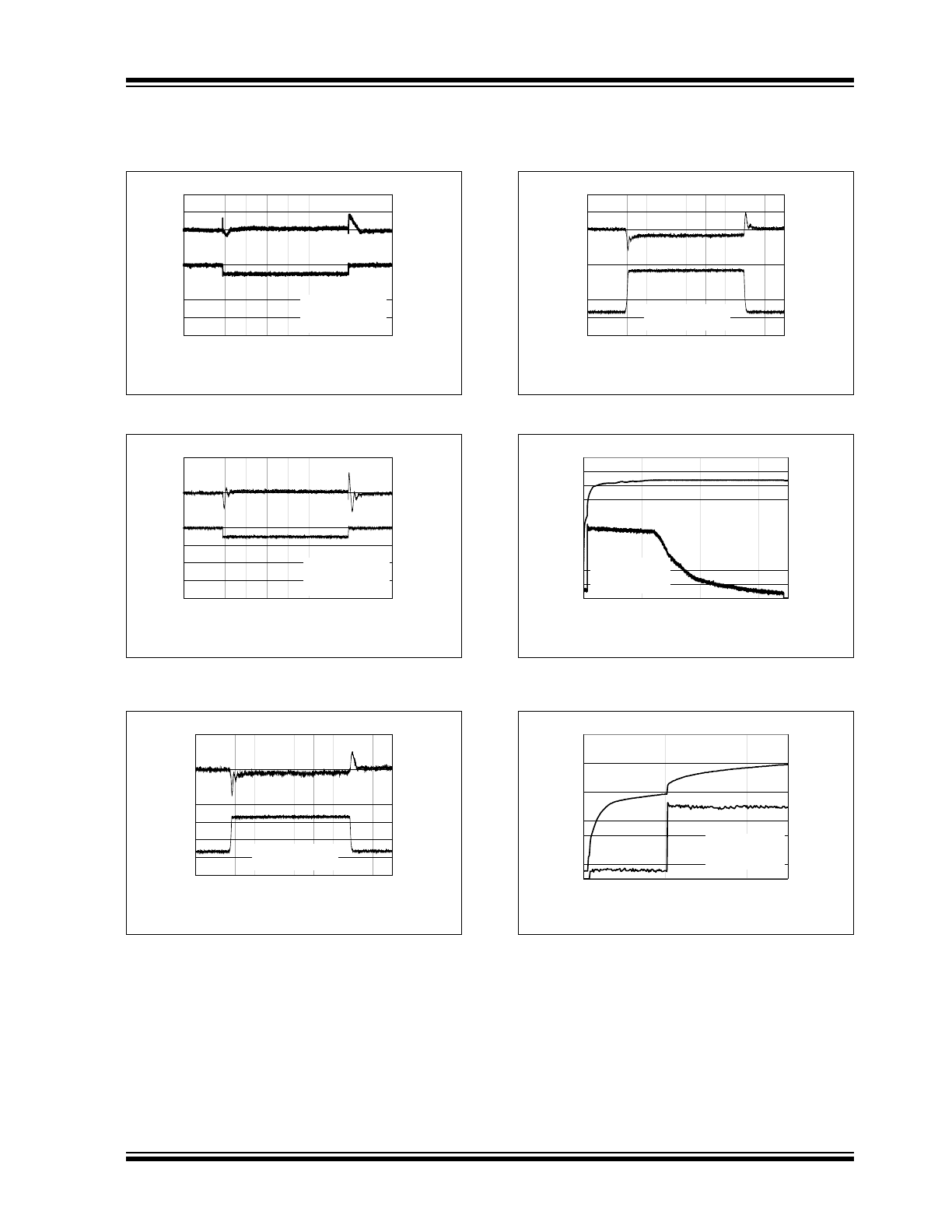
TYPICAL PERFORMANCE CURVES
(Continued)
Note: Unless otherwise indicated, V
DD
= 5.2V, V
REG
= 4.20V, I
OUT
= 10 mA and T
A
= +25°C, Constant-voltage mode.
FIGURE 2-13:
Line Transient Response.
FIGURE 2-14:
Line Transient Response.
FIGURE 2-15:
Load Transient Response.
FIGURE 2-16:
Load Transient Response.
FIGURE 2-17:
Complete Charge Cycle
(180 mA Li-Ion Battery).
FIGURE 2-18:
Charge Cycle Start -
Preconditioning (180 mAh Li-Ion Battery).
-2
0
2
4
6
8
10
12
14
0
20
40
60
80
10
0
12
0
14
0
16
0
18
0
20
0
Time (µs)
Sour
ce Vol
tag
e
(V
)
-0.30
-0.25
-0.20
-0.15
-0.10
-0.05
0.00
0.05
0.10
Ou
tput R
ipple (V)
I
OUT
= 10 mA
C
OUT
= 4.7 µF, X7R
Ceramic
-2
0
2
4
6
8
10
12
14
0
20
40
60
80
10
0
12
0
14
0
16
0
18
0
20
0
Time (µs)
Sour
ce Vol
tag
e
(V
)
-0.30
-0.25
-0.20
-0.15
-0.10
-0.05
0.00
0.05
0.10
Ou
tput R
ipple (V)
I
OUT
= 100 mA
C
OUT
= 4.7 µF, X7R
Ceramic
-0.05
0.00
0.05
0.10
0.15
0.20
0.25
0.30
0.35
0
20
40
60
80
10
0
12
0
14
0
16
0
18
0
20
0
Time (µs)
Output Cur
rent (A
)
-0.12
-0.10
-0.08
-0.06
-0.04
-0.02
0.00
0.02
0.04
O
u
tput Rippl
e (V)
C
OUT
= 4.7 µF, X7R
Ceramic
-0.20
0.00
0.20
0.40
0.60
0.80
1.00
1.20
1.40
0
20
40
60
80
10
0
12
0
14
0
16
0
18
0
20
0
Time (µs)
Output Cur
rent (A
)
-0.30
-0.25
-0.20
-0.15
-0.10
-0.05
0.00
0.05
0.10
Ou
tput R
ipple (V)
C
OUT
= 4.7 µF, X7R
Ceramic
0.0
1.0
2.0
3.0
4.0
5.0
0
30
60
90
120
150
180
210
Time (Minutes)
Battery Voltage (V)
0
40
80
120
160
200
Charge Current (A)
MCP73833-FCI/MF
V
DD
= 5.2V
R
PROG
= 10.0 k:
0.0
1.0
2.0
3.0
4.0
5.0
0
2
4
6
8
10
Time (Minutes)
Battery Voltage (V)
0
40
80
120
160
200
Charge Current (A)
MCP73833-FCI/MF
V
DD
= 5.2V
R
PROG
= 10.0 k:

MCP73833/4
DS22005B-page 10
© 2009 Microchip Technology Inc.
NOTES: