

2014-2017 Microchip Technology Inc.
DS20005139F-page 1
Features
• Single Voltage Read and Write Operations
- 1.65-1.95V
• Serial Interface Architecture
- SPI Compatible: Mode 0 and Mode 3
• High Speed Clock Frequency
- 40MHz
• Superior Reliability
- Endurance: 100,000 Cycles
- Greater than 20 years Data Retention
• Ultra-Low Power Consumption:
- Active Read Current: 4 mA (typical)
- Standby Current: 10 µA (typical)
- Power-down Mode Standby Current: 4 µA (typical)
• Flexible Erase Capability
- Uniform 4 KByte sectors
- Uniform 64 KByte overlay blocks
• Page Program Mode
- 256 Bytes/Page
• Fast Erase and Page-Program:
- Chip-Erase Time: 300 ms (typical)
- Sector-Erase Time: 40 ms (typical)
- Block-Erase Time: 80 ms (typical)
- Page-Program Time: 3 ms/ 256 bytes (typical)
• End-of-Write Detection
- Software polling the BUSY bit in Status Register
• Hold Pin (HOLD#)
- Suspend a serial sequence without
deselecting the device
• Write-Protection (WP#)
- Enables/Disables the Lock-Down function of
the status register
• Software Write-Protection
- Write protection through Block-Protection bits
in status register
• Temperature Range
- Industrial: -40°C to +85°C
• Packages Available
- 8-lead SOIC (150 mils)
- 8-contact USON (2mm x 3mm)
- 8-contact WDFN(5mm x 6mm)
• All devices are RoHS compliant
Product Description
SST25WF020A is a member of the Serial Flash 25
Series family and feature a four-wire, SPI-compatible
interface that allows for a low pin count package which
occupies less board space and ultimately lowers total
system costs. SPI Serial Flash memory is manufac-
tured with proprietary, high performance CMOS
SuperFlash technology. The split-gate cell design and
thick-oxide tunneling injector attain better reliability and
manufacturability compared with alternate approaches.
This Serial Flash significantly improves performance
and reliability, while lowering power consumption. The
device writes (Program or Erase) with a single power
supply of 1.65-1.95V. The total energy consumed is a
function of the applied voltage, current, and time of
application. Since for any given voltage range, the
SuperFlash technology uses less current to program
and has a shorter erase time, the total energy con-
sumed during any Program or Erase operation is less
than alternative Flash memory technologies.
SST25WF020A is offered in 8-lead SOIC, 8-contact
USON, and 8-contact WDFN packages. See
Figure 2-
1
for the pin assignments.
SST25WF020A
2 Mbit 1.8V SPI Serial Flash

SST25WF020A
DS20005139F-page 2
2014-2017 Microchip Technology Inc.
TO OUR VALUED CUSTOMERS
It is our intention to provide our valued customers with the best documentation possible to ensure successful use of your Microchip
products. To this end, we will continue to improve our publications to better suit your needs. Our publications will be refined and
enhanced as new volumes and updates are introduced.
If you have any questions or comments regarding this publication, please contact the Marketing Communications Department via
E-mail at
docerrors@microchip.com
. We welcome your feedback.
Most Current Data Sheet
To obtain the most up-to-date version of this data sheet, please register at our Worldwide Web site at:
http://www.microchip.com
You can determine the version of a data sheet by examining its literature number found on the bottom outside corner of any page.
The last character of the literature number is the version number, (e.g., DS30000000A is version A of document DS30000000).
Errata
An errata sheet, describing minor operational differences from the data sheet and recommended workarounds, may exist for current
devices. As device/documentation issues become known to us, we will publish an errata sheet. The errata will specify the revision
of silicon and revision of document to which it applies.
To determine if an errata sheet exists for a particular device, please check with one of the following:
• Microchip’s Worldwide Web site;
http://www.microchip.com
• Your local Microchip sales office (see last page)
When contacting a sales office, please specify which device, revision of silicon and data sheet (include literature number) you are
using.
Customer Notification System
Register on our web site at
www.microchip.com
to receive the most current information on all of our products.
2014-2017 Microchip Technology Inc.
DS20005139F-page 3
SST25WF020A
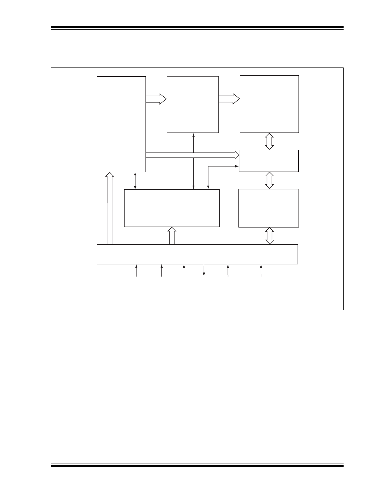
1.0
FUNCTIONAL BLOCK DIAGRAM
FIGURE 1-1:
FUNCTIONAL BLOCK DIAGRAM
25139 F01.0
I/O Buffers
and
Data Latches
SuperFlash
Memory
X - Decoder
Control Logic
Address
Buffers
and
Latches
CE#
Y - Decoder
SCK
SI
SO
WP#
HOLD#
Serial Interface
SST25WF020A
DS20005139F-page 4
2014-2017 Microchip Technology Inc.
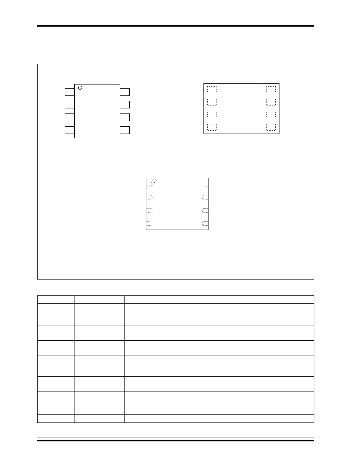
2.0
PIN DESCRIPTION
FIGURE 2-1:
PIN ASSIGNMENTS
TABLE 2-1:
PIN DESCRIPTION
Symbol
Pin Name
Functions
SCK
Serial Clock
To provide the input/output timing of the serial interface.
Commands, addresses, or input data are latched on the rising edge of the clock
input, while output data is shifted out on the falling edge of the clock input.
SI
Serial Data Input
To transfer commands, addresses, or data serially into the device.
Inputs are latched on the rising edge of the serial clock.
SO
Serial Data Output To transfer data serially out of the device.
Data is shifted out on the falling edge of the serial clock.
CE#
Chip Enable
The device is enabled by a high-to-low transition on CE#. CE# must remain low
for the duration of any command sequence. The device is deselected and
placed in Standby mode when CE# is high.
WP#
Write Protect
The Write-Protect (WP#) pin is used to enable/disable BPL bit in the status
register.
HOLD#
Hold
To temporarily stop serial communication with SPI Flash memory while device
is selected.
V
DD
Power Supply
To provide power supply voltage: 1.65-1.95V for SST25WF020A
V
SS
Ground
8-Lead SOIC
8-Contact USON
1
2
3
4
8
7
6
5
CE#
SO
WP#
V
SS
V
DD
HOLD#
SCK
SI
25139 08-soic-P0.0
1
2
3
4
8
7
6
5
CE#
SO
WP#
VSS
Top View
VDD
HOLD#
SCK
SI
25139 08-uson Q3A P1.0
1
2
3
4
8
7
6
5
CE#
SO
WP#
VSS
Top View
VDD
HOLD#
SCK
SI
20005139 08-WDFN MF P1.0
8-Contact WDFN
2014-2017 Microchip Technology Inc.
DS20005139F-page 5
SST25WF020A
3.0
MEMORY ORGANIZATION
The SST25WF020A SuperFlash memory arrays are
organized in 64 uniform 4 KByte sectors, with four
64 KByte overlay erasable blocks.
FIGURE 3-1:
MEMORY MAP
4.0
DEVICE OPERATION
SST25WF020A is accessed through the SPI (Serial
Peripheral Interface) bus compatible protocol. The SPI
bus consist of four control lines; Chip Enable (CE#) is
used to select the device, and data is accessed through
the Serial Data Input (SI), Serial Data Output (SO), and
Serial Clock (SCK).
The SST25WF020A supports both Mode 0 (0,0) and
Mode 3 (1,1) of SPI bus operations. The difference
between the two modes, as shown in
Figure 4-1
, is the
state of the SCK signal when the bus master is in
Standby mode and no data is being transferred. The
SCK signal is low for Mode 0 and SCK signal is high for
Mode 3. For both modes, the Serial Data In (SI) is sam-
pled at the rising edge of the SCK clock signal and the
Serial Data Output (SO) is driven after the falling edge
of the SCK clock signal.
FIGURE 4-1:
SPI PROTOCOL
25139 F51.0
Top of Memory Block
00FFFFH
00F000H
000FFFH
000000H
001FFFH
001000H
Bottom of Memory Block
. . .
01FFFFH
01F000H
01FFFFH
010000H
. . .
. . .
03FFFFH
03F000H
030FFFH
030000H
. . .
Number of Sectors
15
0
1
. . .
31
16
. . .
. . .
63
48
. . .
1
0
. . .
3
Number of 64 KByte
Blocks
25139 F03.0
MODE 3
SCK
SI
SO
CE#
MODE 3
DON'T CARE
Bit 7 Bit 6 Bit 5 Bit 4 Bit 3 Bit 2 Bit 1 Bit 0
Bit 7 Bit 6 Bit 5 Bit 4 Bit 3 Bit 2 Bit 1 Bit 0
MODE 0
MODE 0
HIGH IMPEDANCE
MSB
MSB
SST25WF020A
DS20005139F-page 6
2014-2017 Microchip Technology Inc.
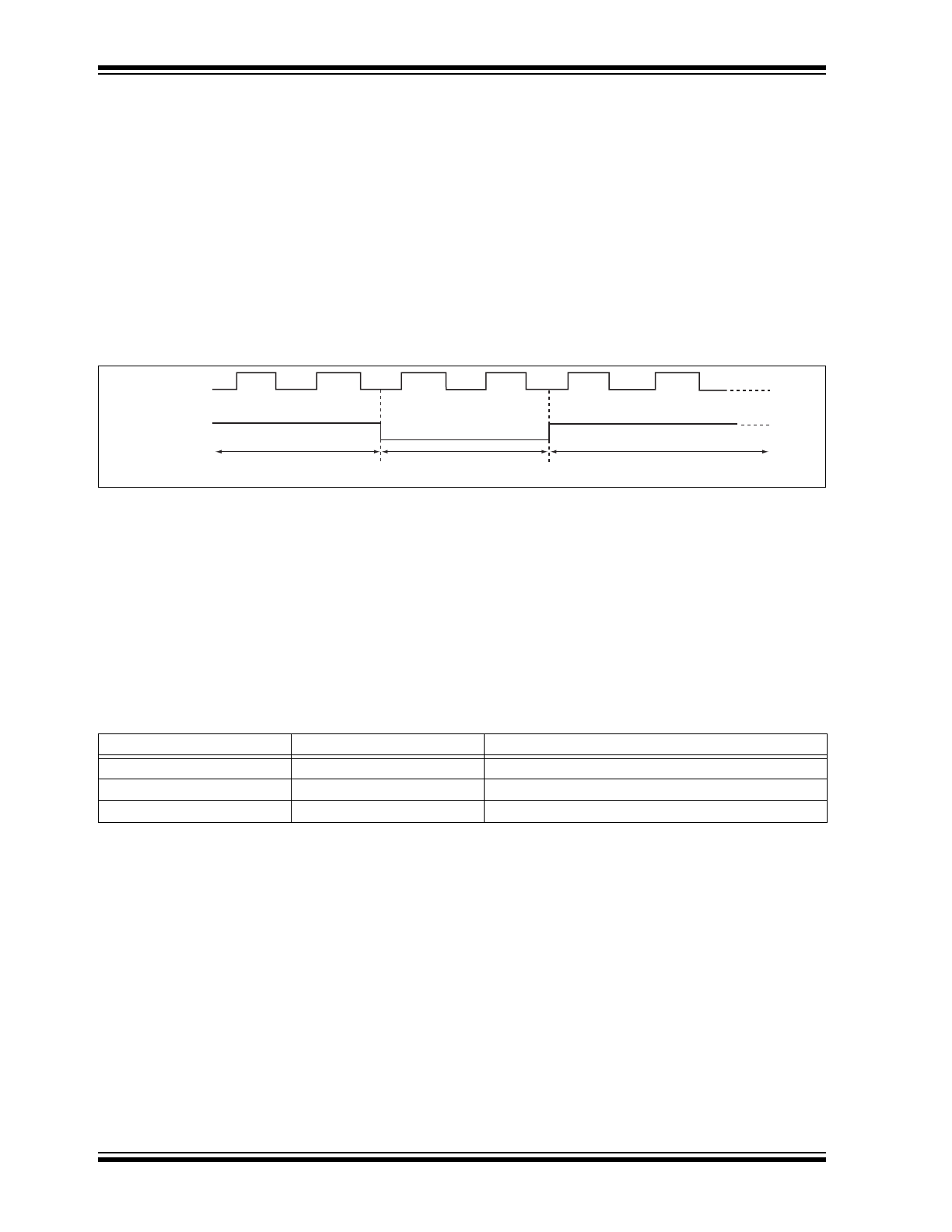
4.0.1
HOLD
In the HOLD# mode, serial sequences underway with
the SPI Flash memory are paused without resetting the
clocking sequence. To activate the HOLD# mode, CE#
must be in active low state. The HOLD# mode begins
when the SCK active low state coincides with the falling
edge of the HOLD# signal. The HOLD# mode ends
when the rising edge of the HOLD# signal coincides
with the SCK active low state. HOLD# must not rise or
fall when SCK logic level is high. See
Figure 4-2
for
Hold Condition waveform.
Once the device enters HOLD# mode, SO will be in
high-impedance state while SI and SCK can be V
IL
or
V
IH.
If CE# is driven active high during a Hold condition, the
device returns to standby mode. The device can then
be re-initiated with the command sequences listed in
Table
5-1
. As long as HOLD# signal is low, the memory
remains in the Hold condition. To resume communica-
tion with the device, HOLD# must be driven active high,
and CE# must be driven active low. See
Figure 4-2
for
Hold timing.
FIGURE 4-2:
HOLD CONDITION WAVEFORM
4.1
Write-Protection
SST25WF020A provides software write-protection. The
Write-Protect pin (WP#) enables or disables the lock-
down function of the status register. The Block-
Protection bits (BP0, BP1, TB, and BPL) in the status
register provide write-protection to the memory array
and the status register. See
Table 4-3
for the Block-Pro-
tection description.
4.1.1
WRITE-PROTECT PIN (WP#)
The Write-Protect (WP#) pin enables the lock-down
function of the BPL bit (bit 7) in the status register.
When WP# is driven low, the execution of the Write-
Status-Register (WRSR) instruction is determined by
the value of the BPL bit (see
Table 4-1
). When WP# is
high, the lock-down function of the BPL bit is disabled.
Active
Hold
Active
25139 F05.1
SCK
HOLD#
TABLE 4-1:
CONDITIONS TO EXECUTE WRITE-STATUS-REGISTER (WRSR) INSTRUCTION
WP#
BPL
Execute WRSR Instruction
L
1
Not Allowed
L
0
Allowed
H
X
Allowed
2014-2017 Microchip Technology Inc.
DS20005139F-page 7
SST25WF020A
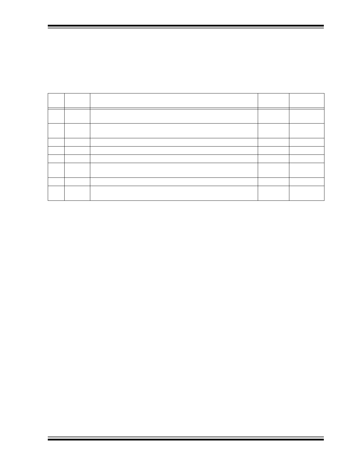
4.2
Status Register
The software status register provides status on
whether the flash memory array is available for any
Read or Write operation, whether the device is Write
enabled, and the state of the Memory Write protection.
During an internal Erase or Program operation, the sta-
tus register may be read only to determine the comple-
tion of an operation in progress.
Table 4-2
describes
the function of each bit in the software status register.
4.2.1
BUSY (BIT 0)
The Busy bit determines whether there is an internal
Erase or Program operation in progress. A ‘1’ for the
Busy bit indicates the device is busy with an operation
in progress. A ‘0’ indicates the device is ready for the
next valid operation.
4.2.2
WRITE-ENABLE-LATCH (WEL–BIT 1)
The Write-Enable-Latch bit indicates the status of the
internal Write-Enable-Latch memory. If the WEL bit is
set to ‘1’, it indicates the device is Write enabled. If the
bit is set to ‘0’ (reset), it indicates the device is not Write
enabled and does not accept any Write (Program/
Erase) commands. The Write-Enable-Latch bit is auto-
matically reset under the following conditions:
• Power-up
• Write-Disable (WRDI) instruction completion
• Page-Program instruction completion
• Sector-Erase instruction completion
• 64 KByte Block-Erase instruction completion
• Chip-Erase instruction completion
• Write-Status-Register instruction completion
4.2.3
BLOCK-PROTECTION (BP0, BP1,
AND TB–BITS 2, 3, AND 5)
The Block-Protection (BP0, BP1, and TB) bits define
the size of the memory area to be software protected
against any memory Write (Program or Erase) opera-
tion, see Table
4-3
. The Write-Status-Register (WRSR)
instruction is used to program the BP0, BP1, and TB
bits as long as WP# is high or the Block-Protect-Lock
(BPL) bit is ‘0’. Chip-Erase can only be executed if
Block-Protection bits are all ‘0’. BP0 and BP1 select the
protected area and TB allocates the protected area to
the higher-order address area (Top Blocks) or lower-
order address area (Bottom Blocks).
TABLE 4-2:
SOFTWARE STATUS REGISTER
Bit
Name
Function
Default at
Power-up
Read/Write
0
BUSY
1 = Internal Write operation is in progress
0 = No internal Write operation is in progress
0
R
1
WEL
1 = Device is memory Write enabled
0 = Device is not memory Write enabled
0
R
2
BP0
1
1. BP0, BP1, TB, and BPL bits are non-volatile memory bits.
Indicate current level of block write-protection (See
Table 4-3
)
0 or 1
R/W
3
BP1
1
Indicate current level of block write-protection (See
Table 4-3
)
0 or 1
R/W
4
RES
Reserved for future use
0
N/A
5
TB
1
1 = 1/4 or 1/2 Bottom Memory Blocks are protected (See
Table 4-3
)
0 = 1/2 or 1/4 Top Memory Blocks are protected
0 or 1
R/W
6
RES
Reserved for future use
0
N/A
7
BPL
1
1 = BP0, BP1, TB, and BPL are read-only bits
0 = BP0, BP1, TB, and BPL are read/writable
0 or 1
R/W
SST25WF020A
DS20005139F-page 8
2014-2017 Microchip Technology Inc.
4.2.4
BLOCK-PROTECTION LOCK-DOWN
(BPL–BIT 7)
When the WP# pin is driven low (V
IL
), it enables the
Block-Protection Lock-Down (BPL) bit. When BPL is
set to ‘1’, it prevents any further alteration of the BP0,
BP1, TB, and BPL bits. When the WP# pin is driven
high (V
IH
), the BPL bit has no effect and its value is
‘Don’t Care’.
TABLE 4-3:
SOFTWARE STATUS REGISTER BLOCK-PROTECTION
Protection Level
Status Register Bit
Protected Memory Address
TB
BP1
BP0
0 (Full Memory Array unprotected)
X
0
0
None
T1 (1/4 Top Memory Block protected)
0
0
1
030000H-03FFFFH
T2 (1/2 Top Memory Block protected)
0
1
0
020000H-03FFFFH
B1 (1/4 Bottom Memory Block protected)
1
0
1
000000H-00FFFFH
B2 (1/2 Bottom Memory Block protected)
1
1
0
000000H-01FFFFH
3 (Full Memory Array protected)
X
1
1
000000H-03FFFFH
2014-2017 Microchip Technology Inc.
DS20005139F-page 9
SST25WF020A
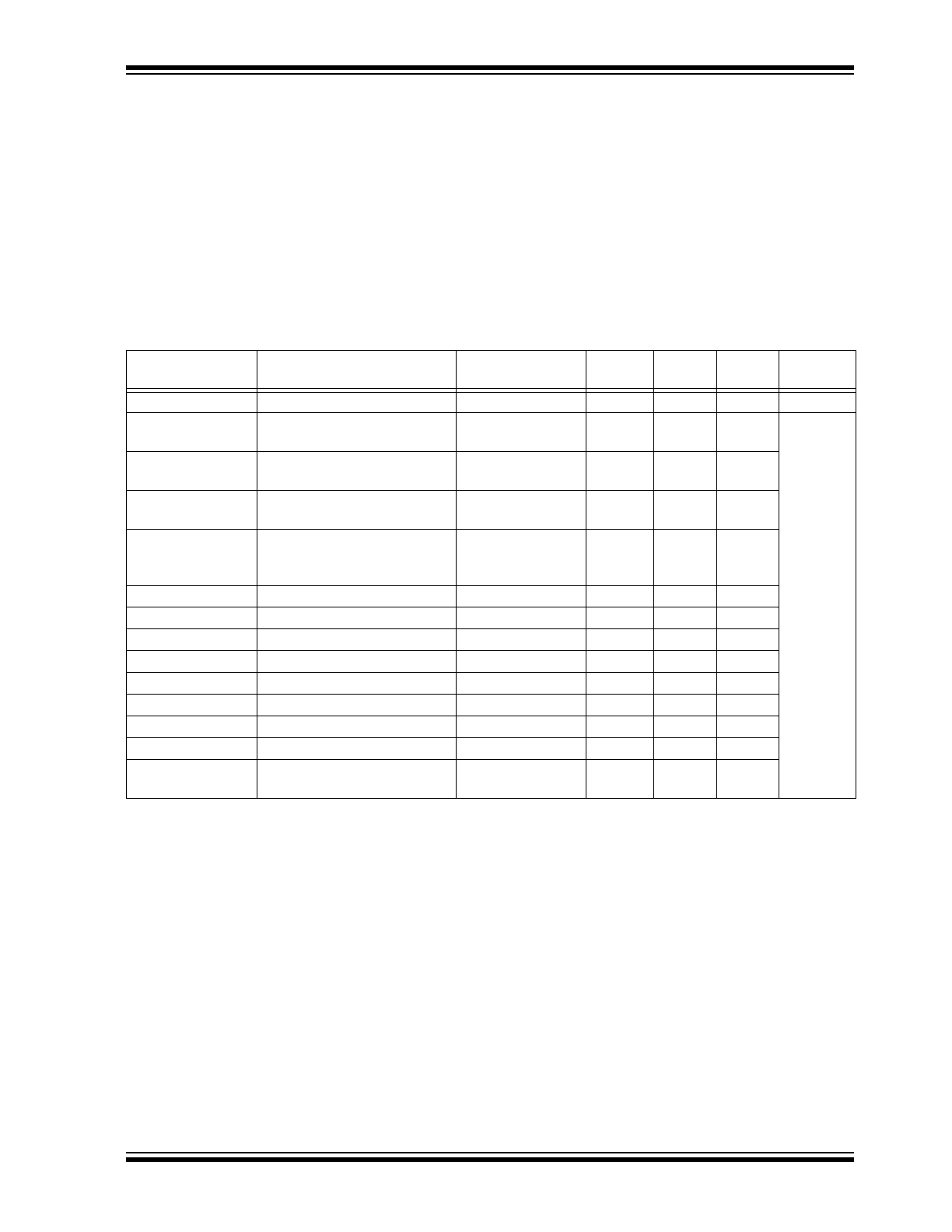
5.0
INSTRUCTIONS
Instructions are used to read, write (Erase and Pro-
gram), and configure the SST25WF020A devices. The
instruction bus cycles are 8 bits each for commands
(Op Code), data, and addresses. The Write-Enable
(WREN) instruction must be executed prior to Sector-
Erase, Block-Erase, Page-Program, Write-Status-Reg-
ister, or Chip-Erase instructions. The complete instruc-
tions are provided in Table
5-1
. All instructions are
synchronized off a high-to-low transition of CE#. Inputs
will be accepted on the rising edge of SCK starting with
the most significant bit. CE# must be driven low before
an instruction is entered and must be driven high after
the last bit of the instruction has been shifted in (except
for Read, Read-ID, and Read-Status-Register instruc-
tions). Any low-to-high transition on CE#, before
receiving the last bit of an instruction bus cycle will
terminate the instruction in progress and return the
device to Standby mode. Instruction commands (Op
Code), addresses and data are all input from the most
significant bit (MSB) first.
TABLE 5-1:
DEVICE OPERATION INSTRUCTIONS
Instruction
Description
Op Code Cycle
1
1. One bus cycle is eight clock periods.
Address
Cycle(s)
2
2. Address bits above the most significant bit of each density can be V
IL
or V
IH
.
Dummy
Cycle(s)
Data
Cycle(s)
Maximum
Frequency
Read
Read Memory
0000 0011b (03H)
3
0
1 to
25 MHz
High-Speed Read
Read Memory at Higher
Speed
0000 1011b (0BH)
3
1
1 to
40 MHz
4 KByte Sector-
Erase
3
3. 4 KByte Sector-Erase addresses: use A
MS
-A
12,
remaining addresses are don’t care but must be set either at V
IL
or V
IH.
Erase 4 KByte of memory
array
0010 0000b (20H)
1101 0111b (D7H)
3
0
0
64 KByte Block-
Erase
4
4. 64 KByte Block-Erase addresses: use A
MS
-A
16,
remaining addresses are don’t care but must be set either at V
IL
or V
IH.
Erase 64 KByte block
of memory array
1101 1000b (D8H)
3
0
0
Chip-Erase
Erase Full Memory Array
0110 0000b (60H)
or
1100 0111b (C7H)
0
0
0
Page-Program
To program up to 256 Bytes
0000 0010b (02H)
3
0
1 to 256
RDSR
5
5. The Read-Status-Register is continuous with ongoing clock cycles until terminated by a low-to-high transition on CE#.
Read-Status-Register
0000 0101b (05H)
0
0
1 to
WRSR
Write-Status-Register
0000 0001b (01H)
0
0
1
WREN
Write-Enable
0000 0110b (06H)
0
0
0
WRDI
Write-Disable
0000 0100b (04H)
0
0
0
RDID
6, 7
6. Device ID is read after three dummy address bytes. The Device ID output stream is continuous until terminated by a low-to-
high transition on CE#.
7. The instructions Release from Deep Power down and Read-ID are similar (ABH). Executing Read-ID requires the ABH
instruction, followed by 24 dummy address bits to retrieve the Device ID. Release from Deep Power-Down only requires the
instruction ABH.
Read-ID
1010 1011b (ABH)
3
0
1 to
JEDEC-ID
JEDEC ID Read
1001 1111b (9FH)
0
0
4 to
DPD
Deep Power-Down Mode
1011 1001b (B9H)
0
0
0
RDPD
7
Release from Deep Power-
Down or Read-ID
1010 1011b (ABH)
0
0
0
SST25WF020A
DS20005139F-page 10
2014-2017 Microchip Technology Inc.
5.1
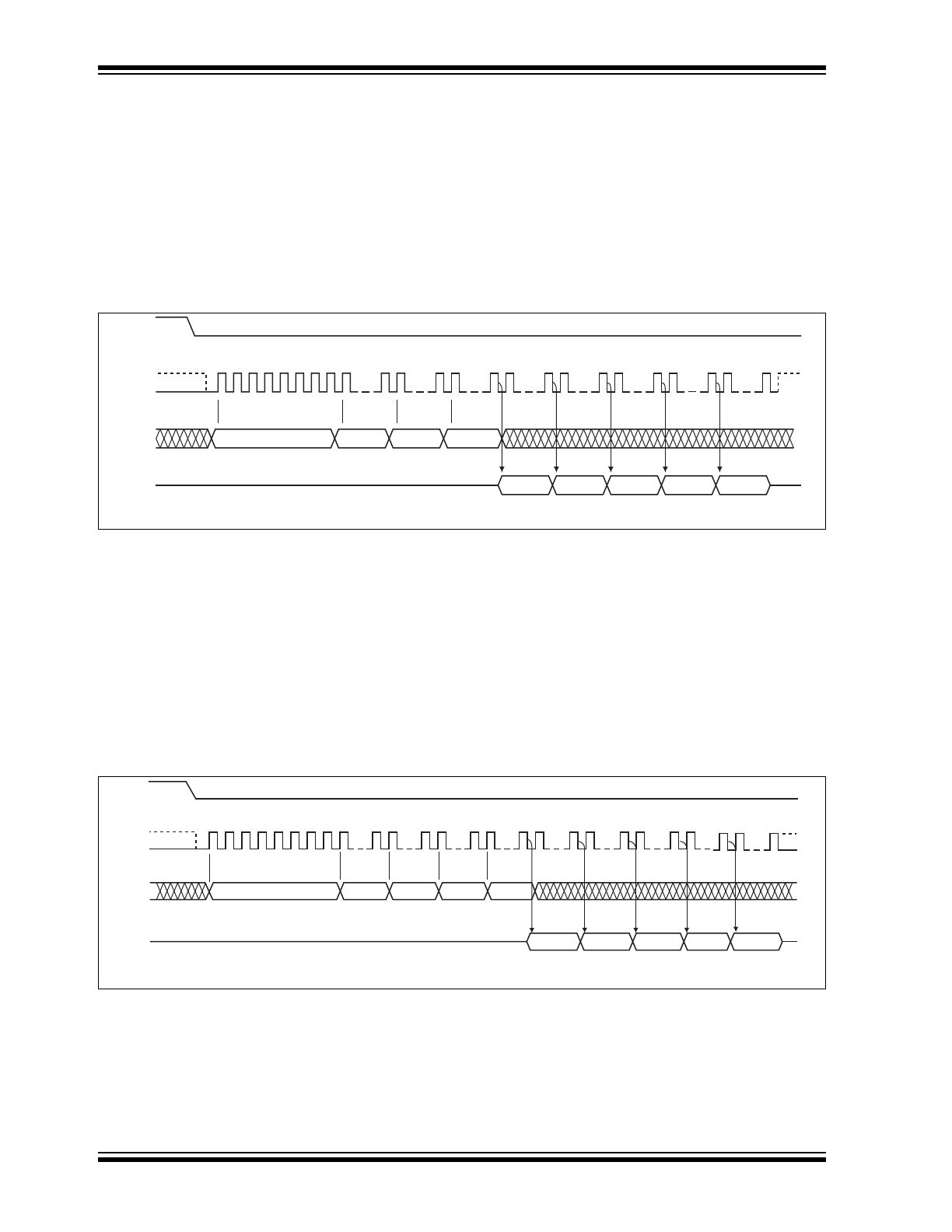
Read (25 MHz)
The Read instruction, 03H, supports up to 25 MHz
Read. The device outputs a data stream starting from
the specified address location. The data stream is con-
tinuous through all addresses until terminated by a low-
to-high transition on CE#. The internal address pointer
automatically increments until the highest memory
address is reached. Once the highest memory address
is reached, the address pointer automatically incre-
ments to the beginning (wrap-around) of the address
space. For example, for 2 Mbit density, once the data
from the address location 3FFFFH is read, the next out-
put is from address location 000000H. The Read
instruction is initiated by executing an 8-bit command,
03H, followed by address bits A
23
-A
0
. CE# must
remain active-low for the duration of the Read cycle.
See
Figure 5-1
for the Read sequence.
FIGURE 5-1:
READ SEQUENCE
5.2
High-Speed-Read (40 MHz)
The High-Speed-Read instruction supporting up to 40
MHz Read is initiated by executing an 8-bit command,
0BH, followed by address bits [A
23
-A
0
] and a dummy
byte. CE# must remain active-low for the duration of
the High-Speed-Read cycle. See
Figure 5-2
for the
High-Speed-Read sequence.
Following a dummy cycle, the High-Speed-Read
instruction outputs the data starting from the specified
address location. The data output stream is continuous
through all addresses until terminated by a low-to-high
transition on CE#. The internal address pointer will
automatically increment until the highest memory
address is reached. Once the highest memory address
is reached, the address pointer will automatically incre-
ment to the beginning (wrap-around) of the address
space. For example, for 2 Mbit density, once the data
from address location 3FFFFH is read, the next output
will be from address location 000000H.
FIGURE 5-2:
HIGH-SPEED-READ SEQUENCE
25139 F06.0
CE#
SO
SI
SCK
ADD.
0 1 2 3 4 5 6 7 8
ADD.
ADD.
03
HIGH IMPEDANCE
15 16
23 24
31 32
39 40
70
47
48
55 56
63 64
N+2
N+3
N+4
N
N+1
D
OUT
MSB
MSB
MSB
MODE 0
MODE 3
D
OUT
D
OUT
D
OUT
D
OUT
25139 F07.0
CE#
SO
SI
SCK
ADD.
0 1 2 3 4 5
6 7 8
ADD.
ADD.
0B
HIGH IMPEDANCE
15 16
23 24
31 32
39 40
47 48
55 56
63 64
N+2
N+3
N+4
N
N+1
X
MSB
MODE 0
MODE 3
D
OUT
D
OUT
D
OUT
D
OUT
80
71 72
D
OUT
MSB