

2015 Microchip Technology Inc.
DS00001885A-page 1
Product Features
• High Performance 32-bit Embedded Controller
• Low power 7.65mA (typ) in active mode
• System in deep sleep consumes 70
μA (typ)
• 3.3-Volt I/O
• Package
- 6mm x 6mm, 28-pin QFN
Sensor Firmware
• Sensor fusion firmware features include:
- Self-contained 9-axis sensor fusion
- Sensor data pass-through
- Fast in-use background calibration of all sen-
sors and calibration monitor
- Magnetic immunity: Enhanced magnetic dis-
tortion detection and suppression
- Gyroscope drift cancellation
• Easy to implement complete turnkey sensor
fusion solution
• Sensor power management
• Sensors Supported
- Bosch BMC150 Geomagnetic Sensor/Accel-
erometer
- Bosch BMG160 Gyroscope
Hardware Features
The hardware features in the SSC7150 motion copro-
cessor include the following:
• Two I
2
C Controllers
- Supports I
2
C bus speeds to 400kHz
- Host Interface Supports Slave Operation
- Sensor Interface Supports Master Operation
• Low Power Modes
Target Markets
• Remote Controls, Gaming
• Fitness Monitoring
• Internet of Things Applications
Description
The SSC7150 motion coprocessor is a low-power, flex-
ible, turnkey solution. SSC7150 makes implementing
sensor fusion easy for motion-based embedded appli-
cations. Microchip created this solution, enabling faster
time to market without the need for sensor-fusion
expertise. The SSC7150 is extremely efficient. Low
average current while running complex sensor-fusion
algorithms results in lower power consumption for mul-
tiple applications.
SSC7150
Motion Coprocessor

SSC7150
DS00001885A-page 2
2015 Microchip Technology Inc.
TO OUR VALUED CUSTOMERS
It is our intention to provide our valued customers with the best documentation possible to ensure successful use of
your Microchip products. To this end, we will continue to improve our publications to better suit your needs. Our pub-
lications will be refined and enhanced as new volumes and updates are introduced.
If you have any questions or comments regarding this publication, please contact the Marketing Communications
Department via E-mail at
docerrors@microchip.com
. We welcome your feedback.
Most Current Data Sheet
To obtain the most up-to-date version of this data sheet, please register at our Worldwide Web site at:
http://www.microchip.com
You can determine the version of a data sheet by examining its literature number found on the bottom outside corner
of any page. The last character of the literature number is the version number, (e.g., DS30000000A is version A of
document DS30000000).
Errata
An errata sheet, describing minor operational differences from the data sheet and recommended workarounds, may
exist for current devices. As device/documentation issues become known to us, we will publish an errata sheet. The
errata will specify the revision of silicon and revision of document to which it applies.
To determine if an errata sheet exists for a particular device, please check with one of the following:
• Microchip’s Worldwide Web site;
http://www.microchip.com
• Your local Microchip sales office (see last page)
When contacting a sales office, please specify which device, revision of silicon and data sheet (include -literature
number) you are using.
Customer Notification System
Register on our web site at
www.microchip.com
to receive the most current information on all of our products.

2015 Microchip Technology Inc.
DS00001885A-page 3
SSC7150
Table of Contents
1.0 Pin Configuration ............................................................................................................................................................................ 4
2.0 System Block Diagram .................................................................................................................................................................. 10
3.0 Guidelines for Getting Started ....................................................................................................................................................... 11
4.0 Electrical Characteristics ............................................................................................................................................................... 14
Appendix A: Revision History .............................................................................................................................................................. 25
The Microchip Web Site ...................................................................................................................................................................... 26
Customer Change Notification Service ............................................................................................................................................... 26
Customer Support ............................................................................................................................................................................... 26
Product Identification System ............................................................................................................................................................. 27
SSC7150
DS00001885A-page 4
2015 Microchip Technology Inc.
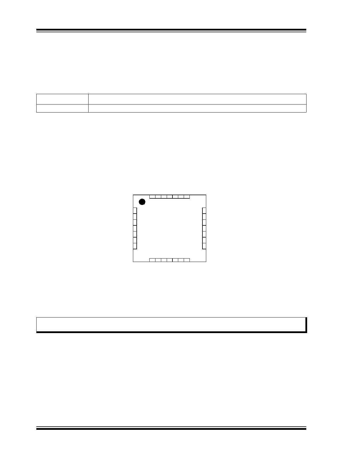
1.0
PIN CONFIGURATION
1.1
Description
The
Pin Configuration
chapter includes a
Pin Diagram
,
Pin List
,
Pin Description
and
Package Details
.
1.2
Terminology and Symbols for Pins/Buffers
1.3
Pin Diagram
FIGURE 1-1:
28 PIN QFN PIN DIAGRAM
Term
Definition
#
The ‘#’ sign at the end of a signal name indicates an active-low signal.
Note:
The metal plane at the bottom of the device is not connected to any pins and is recommended to be con-
nected to VSS externally.
NC
I2
C
2_
R
ESE
T
#
MC
L
R
#
AV
D
D
A
VSS
NC
VS
S
28
27
26
25
24
23
22
NC
1
21
NC
NC
2
20
VDD
I2C_DA2
3
19
NC
I2C_CL2
4
18
NC
VSS
5
17
VCAP
NC
6
16
VSS
I2C_D2_WAKE#
7
15
I2C_DA1
8
9
10
11
12
13
14
I2
C
2_W
A
K
E
VSE
N
S
O
R
_E
N
VD
D
NC
VSS
I2
C2
_A
L
E
RT
#
I2
C
_C
L
1
2015 Microchip Technology Inc.
DS00001885A-page 5
SSC7150
1.4
Pin List
The
Pin List
is shown in
Table 1-1
.
TABLE 1-1:
SSC7150 28 QFN PIN CONFIGURATION
1.4.1
FIVE VOLT TOLERANT PINS
Table 1-2
lists the 5 Volt tolerant pins in the SSC7150. All other pins in the device are 3.3V only.
TABLE 1-2:
5V-TOLERANT PINS
28 QFN
Number
Pin Name
1
NC
2
NC
3
I2C_DA2
4
I2C_CL2
5
VSS
6
NC
7
I2C_D2_WAKE#
8
I2C2_WAKE
9
VSENSOR_EN
10
VDD
11
NC
12
VSS
13
I2C2_ALERT#
14
I2C_CL1
15
I2C_DA1
16
VSS
17
VCAP
18
NC
19
NC
20
VDD
21
NC
22
VSS
23
NC
24
AVSS
25
AVDD
26
MCLR#
27
I2C2_RESET#
28
NC
Pin Number
Pin Name
13
I2C2_ALERT#
14
I2C_CL1
15
I2C_DA1
26
MCLR#
SSC7150
DS00001885A-page 6
2015 Microchip Technology Inc.
1.5
Pin Description
1.5.1
OVERVIEW
The following tables describe the signal functions in the SSC7150 pin configuration. See
Section 1.6, "Notes for Tables
in this Chapter," on page 7
for notes that are referenced in the
Pin Description
tables.
1.5.2
HOST INTERFACE
The SSC7150 can be used with an I
2
C host interface. The pins required for each interface are shown in
Table 1-3
and
Table 1-4
. See the associated Notes for board connection information for the unused interface.
TABLE 1-3:
I
2
C HOST INTERFACE
1.5.3
I
2
C SENSOR INTERFACE
TABLE 1-4:
I
2
C SENSOR INTERFACE
1.5.4
MISCELLANEOUS FUNCTIONS
TABLE 1-5:
MISCELLANEOUS FUNCTIONS
I2C Inte rfa ce S igna ls
P in Re f. Num be r
S igna l Na m e
De scription
Note s
4
I2C_CL2
I2C Controller Clock to Host Interface
3
I2C_DA 2
I2C Controller Data to Host Interface
13
I2C2_A LE RT#
A lert Interrupt s ignal from m otion coprocessor
to Hos t. Used to tell Host data from m otion
coprocess or is ready to be sent out. A ctive low
output.
7
I2C_D2_W A K E #
Used to wake the m otion c oproc ess or from a
low power s tate due to hos t I2C
com m unic ation. A ctive low input. Connec t to
I2C_DA 2.
8
I2C2_W A K E
Used to wake m otion coproces sor from a S leep
state. This signal m ust be driven high at least
11m s prior to sending any I2C traffic to the
m otion coprocessor. A ctive high input.
27
I2C2_RE S E T#
Reset input. Used to reset the host I2C
interface.
I2C Sensor Interface
Pin Ref. Number
Signal Name
Description
Notes
14
I2C_CL1
I2C Controller Clock to Sensor Interface
15
I2C_DA1
I2C Controller Data to Sensor Interface
Miscellaneous Functions
Pin Ref. Number
Signal Name
Description
Notes
26
MCLR#
Master Clear (Reset) Input
Note 1
9
VSENSOR_EN
Sensor voltage switch control output.
1, 2, 6, 11, 18, 19, 21,
23, 28
NC
Pins labelled NC should be left unconnected on
the board
2015 Microchip Technology Inc.
DS00001885A-page 7
SSC7150
1.5.5
POWER INTERFACE
TABLE 1-6:
POWER INTERFACE
1.6
Notes for Tables in this Chapter
Power Interface
Pin Ref. Number
Signal Name
Description
Notes
17
VCAP
Internal Voltage Regulator Capacitor
Note 2
10, 20
VDD
VDD supply
5, 12, 16, 22
VSS
VDD associated ground
25
AVDD
AVDD supply
24
AVSS
AVDD associated ground
Note 1
A pull-up to VDD is required on the MCLR# pin. Use a 10K ohm pull-up resistor.
Note 2
A low-ESR (1 Ohm) capacitor is required on the VCAP pin, which is used to stabilize the internal voltage
regulator output. The VCAP pin must not be connected to VDD, and must have a CEFC capacitor, with at
least a 6V rating, connected to ground. The type can be ceramic or tantalum.
SSC7150
DS00001885A-page 8
2015 Microchip Technology Inc.
1.7
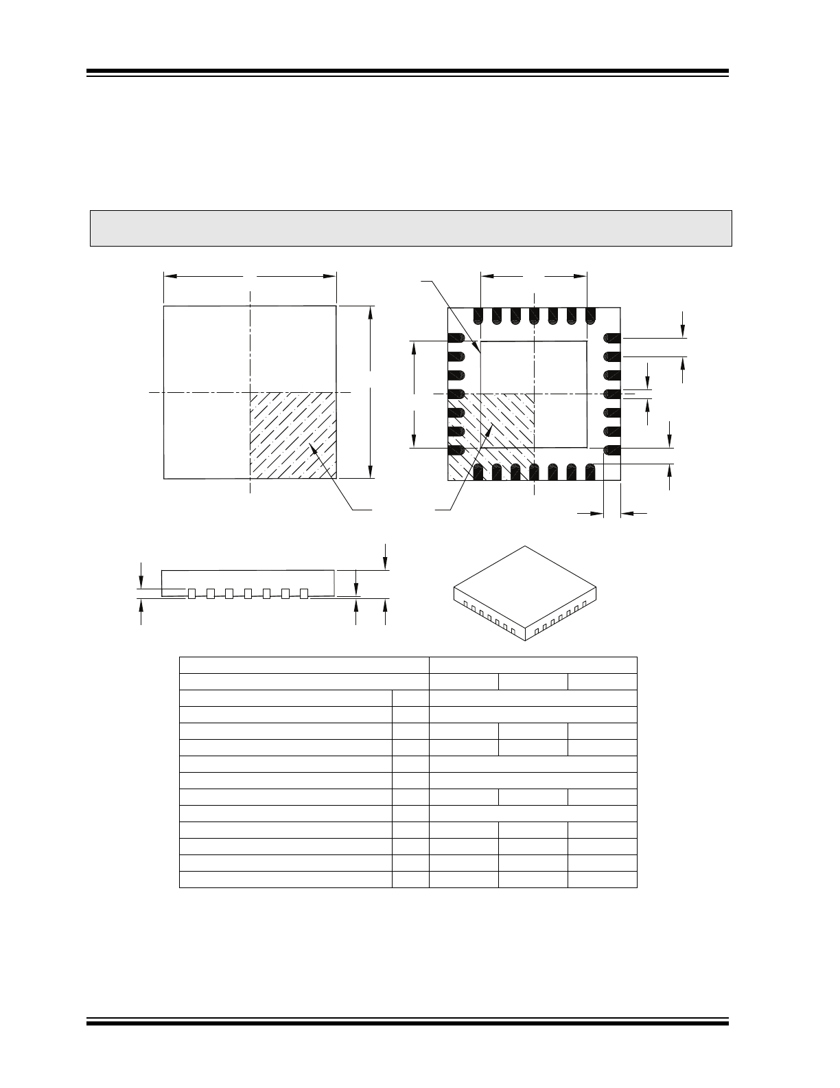
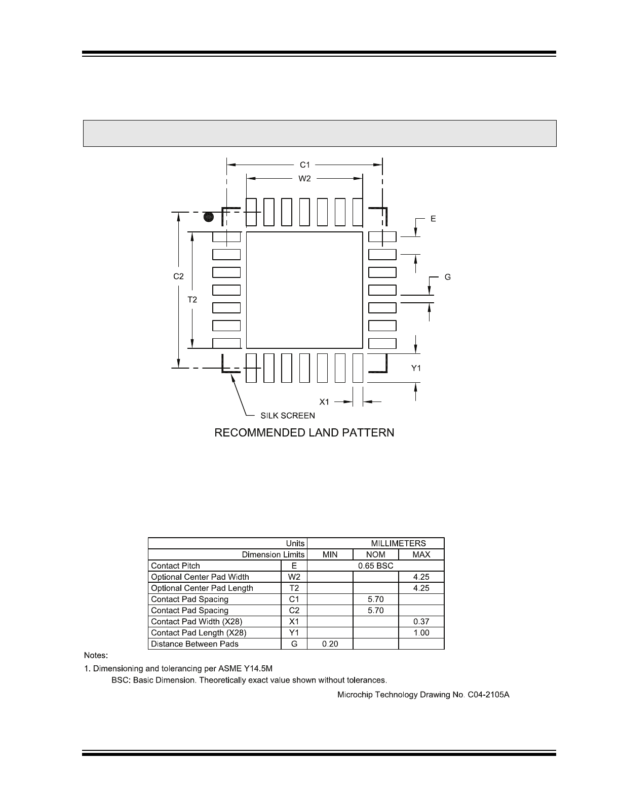
Package Details
This section provides the technical details of the packages.
/HDG3ODVWLF4XDG)ODW1R/HDG3DFNDJH0/±[PP%RG\>4)1@
ZLWKPP&RQWDFW/HQJWK
1RWHV
3LQYLVXDOLQGH[IHDWXUHPD\YDU\EXWPXVWEHORFDWHGZLWKLQWKHKDWFKHGDUHD
3DFNDJHLVVDZVLQJXODWHG
'LPHQVLRQLQJDQGWROHUDQFLQJSHU$60(<0
%6& %DVLF'LPHQVLRQ7KHRUHWLFDOO\H[DFWYDOXHVKRZQZLWKRXWWROHUDQFHV
5() 5HIHUHQFH'LPHQVLRQXVXDOO\ZLWKRXWWROHUDQFHIRULQIRUPDWLRQSXUSRVHVRQO\
1RWH
)RUWKHPRVWFXUUHQWSDFNDJHGUDZLQJVSOHDVHVHHWKH0LFURFKLS3DFNDJLQJ6SHFLILFDWLRQORFDWHGDW
KWWSZZZPLFURFKLSFRPSDFNDJLQJ
8QLWV0,//,0(7(56
'LPHQVLRQ/LPLWV
0,1
120
0$;
1XPEHURI3LQV1
3LWFK
H
%6&
2YHUDOO+HLJKW
$
6WDQGRII
$
&RQWDFW7KLFNQHVV
$
5()
2YHUDOO:LGWK
(
%6&
([SRVHG3DG:LGWK
(
2YHUDOO/HQJWK
'
%6&
([SRVHG3DG/HQJWK
'
&RQWDFW:LGWK
E
&RQWDFW/HQJWK
/
&RQWDFWWR([SRVHG3DG
.
±
±
D
EXPOSED
D2
e
b
K
E2
E
L
N
NOTE 1
1
2
2
1
N
A
A1
A3
TOP VIEW
BOTTOM VIEW
PAD
0LFURFKLS 7HFKQRORJ\ 'UDZLQJ &%
2015 Microchip Technology Inc.
DS00001885A-page 9
SSC7150
/HDG3ODVWLF4XDG)ODW1R/HDG3DFNDJH0/±[PP%RG\>4)1@
ZLWKPP&RQWDFW/HQJWK
1RWH
)RUWKHPRVWFXUUHQWSDFNDJHGUDZLQJVSOHDVHVHHWKH0LFURFKLS3DFNDJLQJ6SHFLILFDWLRQORFDWHGDW
KWWSZZZPLFURFKLSFRPSDFNDJLQJ
SSC7150
DS00001885A-page 10
2015 Microchip Technology Inc.
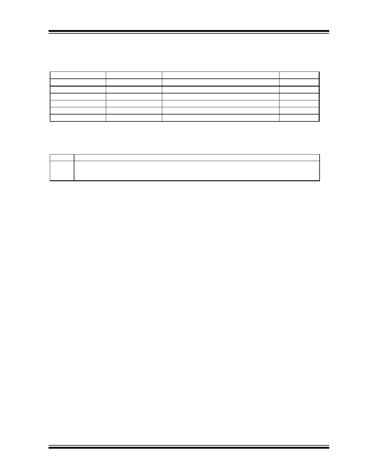
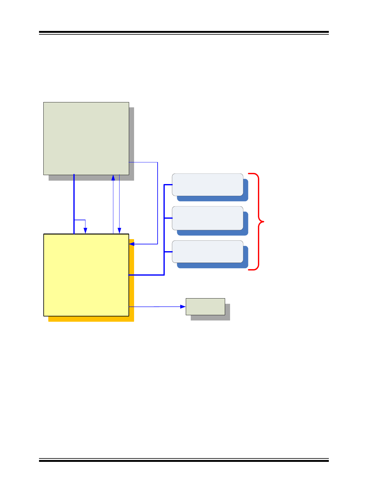
2.0
SYSTEM BLOCK DIAGRAM
The SSC7150 system block diagram is shown in
Figure 2-1
.
FIGURE 2-1:
SSC7150 SYSTEM BLOCK DIAGRAM
SSC7150
Host Processor
3D
MAGNETOMETER
3D
GYROSCOPE
3D
ACCELEROMETER
I2C_DA1/
I2C_CL1
I2C_DA2/
I2C_CL2
9-AXIS SENSOR
FUSION INPUTS
VSENSOR_EN
I2C_D2_WAKE#
I2C2_WAKE
I2C2_ALERT#
Sensor
Power
I2C2_RESET#
2015 Microchip Technology Inc.
DS00001885A-page 1
Product Features
• High Performance 32-bit Embedded Controller
• Low power 7.65mA (typ) in active mode
• System in deep sleep consumes 70
μA (typ)
• 3.3-Volt I/O
• Package
- 6mm x 6mm, 28-pin QFN
Sensor Firmware
• Sensor fusion firmware features include:
- Self-contained 9-axis sensor fusion
- Sensor data pass-through
- Fast in-use background calibration of all sen-
sors and calibration monitor
- Magnetic immunity: Enhanced magnetic dis-
tortion detection and suppression
- Gyroscope drift cancellation
• Easy to implement complete turnkey sensor
fusion solution
• Sensor power management
• Sensors Supported
- Bosch BMC150 Geomagnetic Sensor/Accel-
erometer
- Bosch BMG160 Gyroscope
Hardware Features
The hardware features in the SSC7150 motion copro-
cessor include the following:
• Two I
2
C Controllers
- Supports I
2
C bus speeds to 400kHz
- Host Interface Supports Slave Operation
- Sensor Interface Supports Master Operation
• Low Power Modes
Target Markets
• Remote Controls, Gaming
• Fitness Monitoring
• Internet of Things Applications
Description
The SSC7150 motion coprocessor is a low-power, flex-
ible, turnkey solution. SSC7150 makes implementing
sensor fusion easy for motion-based embedded appli-
cations. Microchip created this solution, enabling faster
time to market without the need for sensor-fusion
expertise. The SSC7150 is extremely efficient. Low
average current while running complex sensor-fusion
algorithms results in lower power consumption for mul-
tiple applications.
SSC7150
Motion Coprocessor
SSC7150
DS00001885A-page 2
2015 Microchip Technology Inc.
TO OUR VALUED CUSTOMERS
It is our intention to provide our valued customers with the best documentation possible to ensure successful use of
your Microchip products. To this end, we will continue to improve our publications to better suit your needs. Our pub-
lications will be refined and enhanced as new volumes and updates are introduced.
If you have any questions or comments regarding this publication, please contact the Marketing Communications
Department via E-mail at
docerrors@microchip.com
. We welcome your feedback.
Most Current Data Sheet
To obtain the most up-to-date version of this data sheet, please register at our Worldwide Web site at:
http://www.microchip.com
You can determine the version of a data sheet by examining its literature number found on the bottom outside corner
of any page. The last character of the literature number is the version number, (e.g., DS30000000A is version A of
document DS30000000).
Errata
An errata sheet, describing minor operational differences from the data sheet and recommended workarounds, may
exist for current devices. As device/documentation issues become known to us, we will publish an errata sheet. The
errata will specify the revision of silicon and revision of document to which it applies.
To determine if an errata sheet exists for a particular device, please check with one of the following:
• Microchip’s Worldwide Web site;
http://www.microchip.com
• Your local Microchip sales office (see last page)
When contacting a sales office, please specify which device, revision of silicon and data sheet (include -literature
number) you are using.
Customer Notification System
Register on our web site at
www.microchip.com
to receive the most current information on all of our products.
2015 Microchip Technology Inc.
DS00001885A-page 3
SSC7150
Table of Contents
1.0 Pin Configuration ............................................................................................................................................................................ 4
2.0 System Block Diagram .................................................................................................................................................................. 10
3.0 Guidelines for Getting Started ....................................................................................................................................................... 11
4.0 Electrical Characteristics ............................................................................................................................................................... 14
Appendix A: Revision History .............................................................................................................................................................. 25
The Microchip Web Site ...................................................................................................................................................................... 26
Customer Change Notification Service ............................................................................................................................................... 26
Customer Support ............................................................................................................................................................................... 26
Product Identification System ............................................................................................................................................................. 27
SSC7150
DS00001885A-page 4
2015 Microchip Technology Inc.
1.0
PIN CONFIGURATION
1.1
Description
The
Pin Configuration
chapter includes a
Pin Diagram
,
Pin List
,
Pin Description
and
Package Details
.
1.2
Terminology and Symbols for Pins/Buffers
1.3
Pin Diagram
FIGURE 1-1:
28 PIN QFN PIN DIAGRAM
Term
Definition
#
The ‘#’ sign at the end of a signal name indicates an active-low signal.
Note:
The metal plane at the bottom of the device is not connected to any pins and is recommended to be con-
nected to VSS externally.
NC
I2
C
2_
R
ESE
T
#
MC
L
R
#
AV
D
D
A
VSS
NC
VS
S
28
27
26
25
24
23
22
NC
1
21
NC
NC
2
20
VDD
I2C_DA2
3
19
NC
I2C_CL2
4
18
NC
VSS
5
17
VCAP
NC
6
16
VSS
I2C_D2_WAKE#
7
15
I2C_DA1
8
9
10
11
12
13
14
I2
C
2_W
A
K
E
VSE
N
S
O
R
_E
N
VD
D
NC
VSS
I2
C2
_A
L
E
RT
#
I2
C
_C
L
1
2015 Microchip Technology Inc.
DS00001885A-page 5
SSC7150
1.4
Pin List
The
Pin List
is shown in
Table 1-1
.
TABLE 1-1:
SSC7150 28 QFN PIN CONFIGURATION
1.4.1
FIVE VOLT TOLERANT PINS
Table 1-2
lists the 5 Volt tolerant pins in the SSC7150. All other pins in the device are 3.3V only.
TABLE 1-2:
5V-TOLERANT PINS
28 QFN
Number
Pin Name
1
NC
2
NC
3
I2C_DA2
4
I2C_CL2
5
VSS
6
NC
7
I2C_D2_WAKE#
8
I2C2_WAKE
9
VSENSOR_EN
10
VDD
11
NC
12
VSS
13
I2C2_ALERT#
14
I2C_CL1
15
I2C_DA1
16
VSS
17
VCAP
18
NC
19
NC
20
VDD
21
NC
22
VSS
23
NC
24
AVSS
25
AVDD
26
MCLR#
27
I2C2_RESET#
28
NC
Pin Number
Pin Name
13
I2C2_ALERT#
14
I2C_CL1
15
I2C_DA1
26
MCLR#
SSC7150
DS00001885A-page 6
2015 Microchip Technology Inc.
1.5
Pin Description
1.5.1
OVERVIEW
The following tables describe the signal functions in the SSC7150 pin configuration. See
Section 1.6, "Notes for Tables
in this Chapter," on page 7
for notes that are referenced in the
Pin Description
tables.
1.5.2
HOST INTERFACE
The SSC7150 can be used with an I
2
C host interface. The pins required for each interface are shown in
Table 1-3
and
Table 1-4
. See the associated Notes for board connection information for the unused interface.
TABLE 1-3:
I
2
C HOST INTERFACE
1.5.3
I
2
C SENSOR INTERFACE
TABLE 1-4:
I
2
C SENSOR INTERFACE
1.5.4
MISCELLANEOUS FUNCTIONS
TABLE 1-5:
MISCELLANEOUS FUNCTIONS
I2C Inte rfa ce S igna ls
P in Re f. Num be r
S igna l Na m e
De scription
Note s
4
I2C_CL2
I2C Controller Clock to Host Interface
3
I2C_DA 2
I2C Controller Data to Host Interface
13
I2C2_A LE RT#
A lert Interrupt s ignal from m otion coprocessor
to Hos t. Used to tell Host data from m otion
coprocess or is ready to be sent out. A ctive low
output.
7
I2C_D2_W A K E #
Used to wake the m otion c oproc ess or from a
low power s tate due to hos t I2C
com m unic ation. A ctive low input. Connec t to
I2C_DA 2.
8
I2C2_W A K E
Used to wake m otion coproces sor from a S leep
state. This signal m ust be driven high at least
11m s prior to sending any I2C traffic to the
m otion coprocessor. A ctive high input.
27
I2C2_RE S E T#
Reset input. Used to reset the host I2C
interface.
I2C Sensor Interface
Pin Ref. Number
Signal Name
Description
Notes
14
I2C_CL1
I2C Controller Clock to Sensor Interface
15
I2C_DA1
I2C Controller Data to Sensor Interface
Miscellaneous Functions
Pin Ref. Number
Signal Name
Description
Notes
26
MCLR#
Master Clear (Reset) Input
Note 1
9
VSENSOR_EN
Sensor voltage switch control output.
1, 2, 6, 11, 18, 19, 21,
23, 28
NC
Pins labelled NC should be left unconnected on
the board
2015 Microchip Technology Inc.
DS00001885A-page 7
SSC7150
1.5.5
POWER INTERFACE
TABLE 1-6:
POWER INTERFACE
1.6
Notes for Tables in this Chapter
Power Interface
Pin Ref. Number
Signal Name
Description
Notes
17
VCAP
Internal Voltage Regulator Capacitor
Note 2
10, 20
VDD
VDD supply
5, 12, 16, 22
VSS
VDD associated ground
25
AVDD
AVDD supply
24
AVSS
AVDD associated ground
Note 1
A pull-up to VDD is required on the MCLR# pin. Use a 10K ohm pull-up resistor.
Note 2
A low-ESR (1 Ohm) capacitor is required on the VCAP pin, which is used to stabilize the internal voltage
regulator output. The VCAP pin must not be connected to VDD, and must have a CEFC capacitor, with at
least a 6V rating, connected to ground. The type can be ceramic or tantalum.
SSC7150
DS00001885A-page 8
2015 Microchip Technology Inc.
1.7
Package Details
This section provides the technical details of the packages.
/HDG3ODVWLF4XDG)ODW1R/HDG3DFNDJH0/±[PP%RG\>4)1@
ZLWKPP&RQWDFW/HQJWK
1RWHV
3LQYLVXDOLQGH[IHDWXUHPD\YDU\EXWPXVWEHORFDWHGZLWKLQWKHKDWFKHGDUHD
3DFNDJHLVVDZVLQJXODWHG
'LPHQVLRQLQJDQGWROHUDQFLQJSHU$60(<0
%6& %DVLF'LPHQVLRQ7KHRUHWLFDOO\H[DFWYDOXHVKRZQZLWKRXWWROHUDQFHV
5() 5HIHUHQFH'LPHQVLRQXVXDOO\ZLWKRXWWROHUDQFHIRULQIRUPDWLRQSXUSRVHVRQO\
1RWH
)RUWKHPRVWFXUUHQWSDFNDJHGUDZLQJVSOHDVHVHHWKH0LFURFKLS3DFNDJLQJ6SHFLILFDWLRQORFDWHGDW
KWWSZZZPLFURFKLSFRPSDFNDJLQJ
8QLWV0,//,0(7(56
'LPHQVLRQ/LPLWV
0,1
120
0$;
1XPEHURI3LQV1
3LWFK
H
%6&
2YHUDOO+HLJKW
$
6WDQGRII
$
&RQWDFW7KLFNQHVV
$
5()
2YHUDOO:LGWK
(
%6&
([SRVHG3DG:LGWK
(
2YHUDOO/HQJWK
'
%6&
([SRVHG3DG/HQJWK
'
&RQWDFW:LGWK
E
&RQWDFW/HQJWK
/
&RQWDFWWR([SRVHG3DG
.
±
±
D
EXPOSED
D2
e
b
K
E2
E
L
N
NOTE 1
1
2
2
1
N
A
A1
A3
TOP VIEW
BOTTOM VIEW
PAD
0LFURFKLS 7HFKQRORJ\ 'UDZLQJ &%
2015 Microchip Technology Inc.
DS00001885A-page 9
SSC7150
/HDG3ODVWLF4XDG)ODW1R/HDG3DFNDJH0/±[PP%RG\>4)1@
ZLWKPP&RQWDFW/HQJWK
1RWH
)RUWKHPRVWFXUUHQWSDFNDJHGUDZLQJVSOHDVHVHHWKH0LFURFKLS3DFNDJLQJ6SHFLILFDWLRQORFDWHGDW
KWWSZZZPLFURFKLSFRPSDFNDJLQJ
SSC7150
DS00001885A-page 10
2015 Microchip Technology Inc.
2.0
SYSTEM BLOCK DIAGRAM
The SSC7150 system block diagram is shown in
Figure 2-1
.
FIGURE 2-1:
SSC7150 SYSTEM BLOCK DIAGRAM
SSC7150
Host Processor
3D
MAGNETOMETER
3D
GYROSCOPE
3D
ACCELEROMETER
I2C_DA1/
I2C_CL1
I2C_DA2/
I2C_CL2
9-AXIS SENSOR
FUSION INPUTS
VSENSOR_EN
I2C_D2_WAKE#
I2C2_WAKE
I2C2_ALERT#
Sensor
Power
I2C2_RESET#