
2017 Microchip Technology Inc.
DS20005544A-page 1
SR086/SR087
Features
• Efficient Operation without Magnetics
• No High-voltage Capacitors
• Adjustable Main Output Voltage (9V to 50V)
• Additional Internal Linear Regulator:
- 3.3V for SR086
- 5V for SR087
• Up to 100 mA Combined Output Current
• Single BOM for 120 VAC/230 VAC
• Built-in Soft Start
• Less than 200 mW Standby Power
Applications
• White Goods
• Household Appliances
• Lighting Controls
• Circuit Breakers
• Keep-alive Supplies
General Description
The SR086/SR087 are inductorless switching
regulators designed to operate directly from a rectified
AC line. The operating principle is to turn on a pass
transistor when the rectified AC is below the output
voltage and to turn it off when the output voltage
reaches a specific level. The ICs feature an adjustable
main output voltage of 9V to 50V and an additional
fixed output of 3.3V for SR086 and 5V for SR087.
Efficiencies of around 55% may be realized for loads
up to 1W in 120 VAC applications and about 50%
efficiencies for loads up to 800 mW in 230 VAC
applications.
A logic-level enable input allows the SR086/SR087 to
be disabled—useful when they are employed as
keep-alive power supplies.
Package Type
Backside on the SOIC package is at ground potential and may be connected to
ground or left unconnected. See
Table 2-1
for pin information.
8-lead SOIC
(with Heat Slug)
(Top view)
1
2
3
4
8
7
6
5
VIN
EN
GND
VREG
GATE
VGD
VOUT
VFB
Heat Slug
WARNING
Galvanic isolation is not provided. Dangerous voltages are present when connected to the AC line. It is
the responsibility of the designer using the SR086/SR087 to ensure that adequate security measures are
in place to protect the end user from electrical shock.
The circuits shown in this data sheet are not guaranteed to meet surge and conducted EMI
requirements. The effectiveness of these circuits may vary with a particular application. The designer
must conduct tests to ascertain compliance with applicable standards and regulations.
Adjustable Offline Inductorless Switching Regulators
SR086/SR087
DS20005544A-page 2
2017 Microchip Technology Inc.
Functional Block Diagram
1.0kV
1.0A
275V
50A
90 to
270VAC
50/60Hz
R
GD
1.1MΩ
STGD5NB120SZ
V
OUT
- 1
1.25V
R
FB(HI)
= R
FB(LO)
3.3V
C
REG
100nF
GND
VREG
FB
VOUT
VGD
GATE
VIN
EN
1.25A
9.0 - 50VDC
SR086
R
FB(LO)
12.4k
Ω
C
GD
100nF
C
OUT
470μF
R
PD
390kΩ
C
OUT1
1.0μF
Upper circuitry
powered by V
GD
- V
OUT
Lower circuitry
powered by V
OUT
- GND
Level
Translator
1.25V
REG
R
Q
S
13V
s
1.0kV
1.0A
275V
50A
90 to
270VAC
50/60Hz
R
GD
1.1MΩ
STGD5NB120SZ
V
OUT
- 1
1.25V
R
FB(HI)
= R
FB(LO)
5.0V
C
REG
100nF
GND
VREG
FB
VOUT
VGD
GATE
VIN
EN
1.25A
9.0 - 50VDC
SR087
R
FB(LO)
12.4k
Ω
C
GD
100nF
C
OUT
470μF
R
PD
390kΩ
C
OUT
1
1.0μF
Upper circuitry
powered by V
GD
- V
OUT
Lower circuitry
powered by V
OUT
- GND
Level
Translator
1.25V
REG
R
Q
S
13V
2017 Microchip Technology Inc.
DS20005544A-page 3
SR086/SR087
Typical Application
1.0kV
1.0A
275V
50A
90 to
270VAC
50/60Hz
390kΩ
1.1MΩ
STGD5NB120SZ
V
OUT
- 1
1.25V
R
1
= R
2
3.3V
@60mA
100nF
GND
VREG
FB
VOUT
VGD
GATE
VIN
EN
Enable
1.25A
V
OUT
9.0 - 50VDC
@100mA - I
REG
SR086
R
2
12.4k
Ω
1.0μF
100nF
470μF
Circuits
1.0kV
1.0A
275V
50A
90 -
270VAC
50/60Hz
390kΩ
1.1MΩ
STGD5NB120SZ
V
OUT
- 1
1.25V
R
1
= R
2
5.0V
@60mA
100nF
GND
VREG
FB
VOUT
VGD
GATE
VIN
EN
Enable
1.25A
V
OUT
9.0 - 50VDC
@ 100mA - I
REG
SR087
R
2
12.4k
Ω
1.0μF
100nF
470μF
SR086/SR087
DS20005544A-page 4
2017 Microchip Technology Inc.
1.0
ELECTRICAL CHARACTERISTICS
Absolute Maximum Ratings †
Output Voltage, V
OUT
..................................................................................................................................–0.3V to 56V
Feedback Voltage, V
FB
..............................................................................................................................–0.3V to 6.5V
Enable Voltage, V
EN
...................................................................................................................................–0.3V to 6.5V
Operating Junction Temperature, T
J
.................................................................................................... –40°C to +125°C
† Notice: Stresses above those listed under “Absolute Maximum Ratings” may cause permanent damage to the
device. This is a stress rating only, and functional operation of the device at those or any other conditions above those
indicated in the operational sections of this specification is not intended. Exposure to maximum rating conditions for
extended periods may affect device reliability.
RECOMMENDED OPERATING CONDITIONS
Parameter
Sym.
Min.
Typ.
Max.
Unit
Conditions
Output Voltage
V
OUT
9
—
50
V
Load on V
OUT
, including Feedback Divider and Load on V
REG
I
OUT
100
—
—
µA
Headroom for Internal Linear Regulation (V
OUT
–V
REG
)
V
HR
4
—
—
V
ELECTRICAL CHARACTERISTICS
Electrical Specifications: Unless otherwise noted, T
A
= –40°C to +85°C. Voltages referenced to GND pin.
Parameter
Sym.
Min.
Typ.
Max.
Unit
Conditions
Current Consumption at V
GD
I
GD
—
—
60
µA
Current Consumption of the Lower Circuitry
I
OUT(INT)
—
—
400
µA
V
OUT
= 9V–50V
Gate Drive Supply Voltage
V
GD
11
13
15
V
Note 1
Gate Output High Voltage
V
GATE(HI)
11
—
15
V
Note 1
Gate Output Low Voltage
V
GATE(LO)
—
—
0.5
V
Note 1
Feedback Voltage (Gate Off)
V
FB(OFF)
1.18
1.25
1.31
V
Feedback Voltage (Hysteresis)
V
FB(HYST)
—
50
—
mV
Feedback Input Current
I
FB
—
—
500
nA
V
IN
Trip Voltage (Gate On)
V
TRIP(ON)
0
—
3
V
Note 1
V
IN
Trip Voltage (Gate Off)
V
TRIP(OFF)
9
—
15
V
Note 1
Enable Voltage, On
V
EN(ON)
0.2
—
—
V
Enable Voltage, Off
V
EN(OFF)
—
—
0.75
V
REG
V
IN
Gate Turn-on Delay
t
DIG(ON)
0
—
1
µs
C
GATE
= 1 nF
V
IN
Gate Turn-off Delay
t
DIG(OFF)
—
—
600
ns
C
GATE
= 1 nF
Feedback Gate Turn-off Delay
t
DFG(OFF)
—
—
450
ns
C
GATE
= 1 nF, V
FB
= 1.5V
Regulated Output Voltage
SR086
V
REG
3.125
3.3
3.465
V
I
LOAD
= 1 mA, V
OUT
= 9V
SR087
4.750
5
5.250
V
V
REG
Load Regulation
Δ
I
V
REG
–50
—
+50
mV
0 mA < I
LOAD
< 60 mA,
V
OUT
= 9V, T
AMB
= 25°C
Gate V
GD
Diode Drop
V
D
—
—
1
V
I = 20 mA
Note 1: Referenced to V
OUT
TEMPERATURE CHARACTERISTICS
Electrical Characteristics: Unless otherwise noted, for all specifications T
A
=T
J
= +25°C.
Parameter
Sym.
Min. Typ.
Max.
Unit
Conditions
TEMPERATURE RANGE
Operating Junction Temperature
T
J
–40
—
+125
°C
PACKAGE THERMAL RESITANCE
8-lead SOIC (with Heat Slug)
θ
JA
—
84
—
°C/W
2017 Microchip Technology Inc.
DS20005544A-page 5
SR086/SR087
SR086/SR087
DS20005544A-page 6
2017 Microchip Technology Inc.
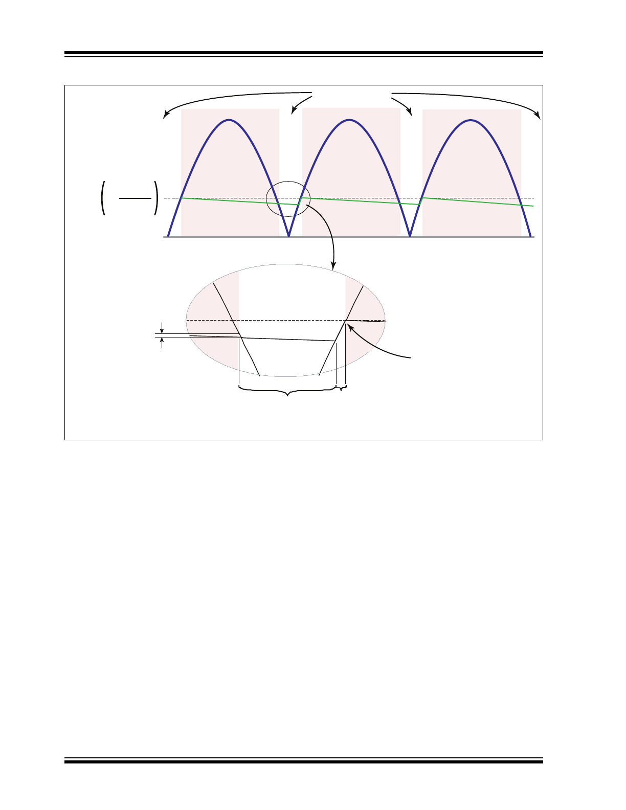
SRO86 and SR087 Timing Diagram
Pass Transistor on
V
IN
V
OUT
not to scale
V
FB(OFF)
1+
RF
B(HI)
RF
B(LO)
Pass Transistor is turned
on when V
IN
falls below:
V
OUT
+ V
TRIP(ON)
Pass Transistor is on but
not conducting since the
input voltage is lower
than the output voltage
Pass Transistor is on
and conducting
Pass Transistor is
turned off once V
OUT
reaches the trip point
2017 Microchip Technology Inc.
DS20005544A-page 7
SR086/SR087
2.0
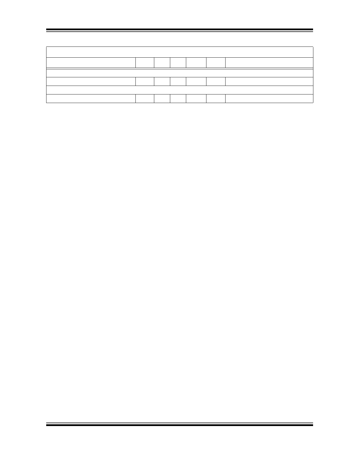
PIN DESCRIPTION
The descriptions of the SR086/SR087 pins are listed
on
Table 2-1
. Refer to
Package Type
for the location of
pins.
TABLE 2-1:
PIN FUNCTION TABLE
Pin Number
SR086
Pin Name
SR087
Pin Name
Description
1
VIN
VIN
Rectified AC input voltage
2
EN
EN
Active low enable input
3
GND
GND
Circuit ground (
Note 1
)
4
VREG
VREG
Regulated output voltage (
Note 2
)
5
FB
FB
Feedback input
6
VOUT
VOUT
Output voltage (9V–50V adj.)
7
VGD
VGD
Gate drive supply (referenced to VOUT)
8
GATE
GATE
Drives external IGBT pass transistor
Note 1: Circuit ground will be at the AC line potential.
2: Fixed 3.3V for SR086 and fixed 5V for SR087
SR086/SR087
DS20005544A-page 8
2017 Microchip Technology Inc.
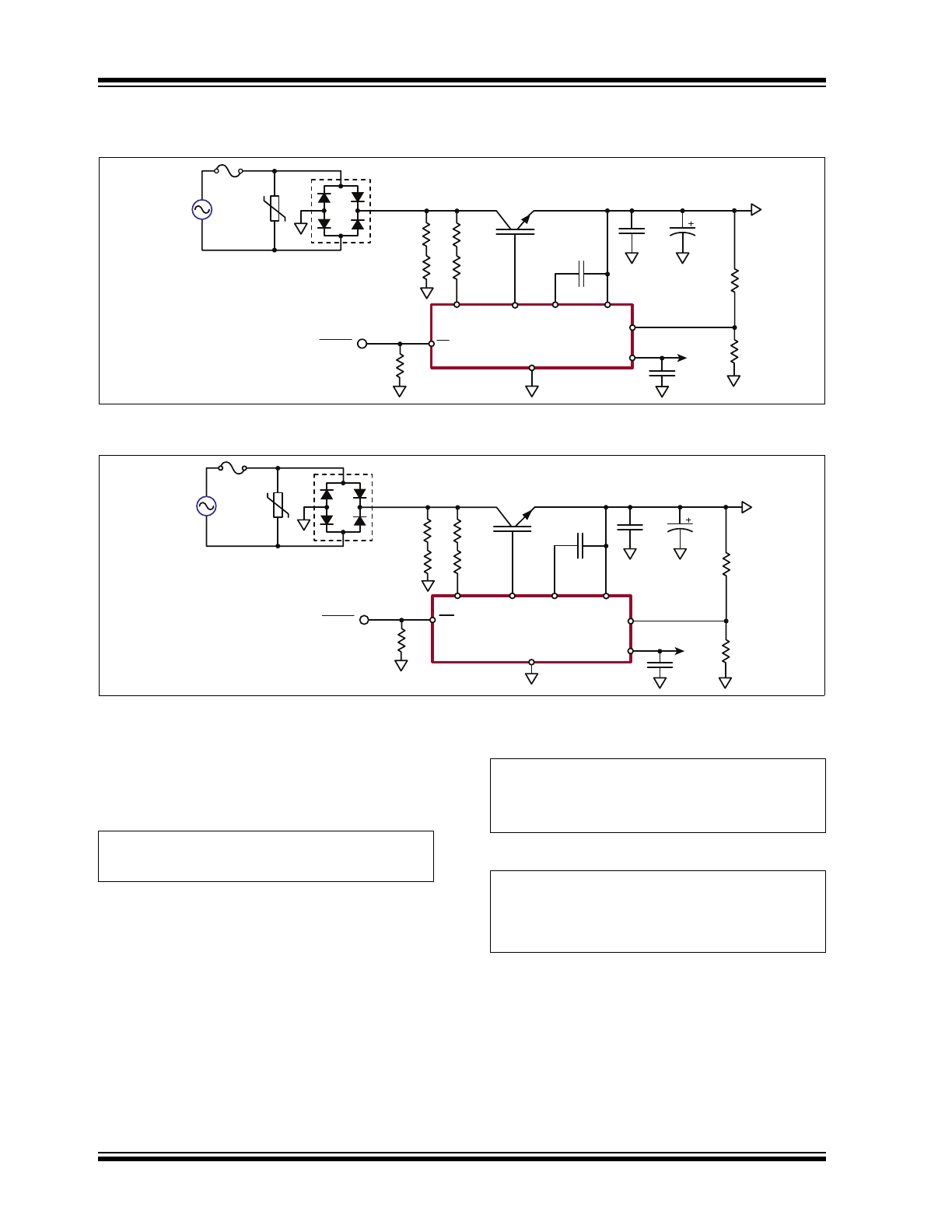
3.0
APPLICATION INFORMATION
D
1
1.0kV
1.0A
Z
1
275V
50A
V
IN
90 to 270VAC
50/60Hz
F
1
1.0A
R
6
12.4k
Ω
R
5
113k
Ω
V
OUT
12.6VDC
*R
4
510k
Ω
*R
3
510k
Ω
*R
1
200k
Ω
*R
2
200k
Ω
* Two resistors used in
series for reasons of
high voltage creepage
and resistor voltage rating.
Enable
R
7
100k
Ω
C
2
1.0μF
C
3
470μF
C
1
100nF
C
4
100nF
V
REG
3.3VDC
Q
1
STGD5NB120SZ
VIN
GATE
VGD
VOUT
FB
VREG
GND
EN
2
3
4
5
6
7
8
1
SR086
FIGURE 3-1:
SR086 Typical Application Circuit.
D
1
1.0kV
1.0A
Z
1
275V
50A
V
IN
90 to 270VAC
50/60Hz
F
1
1.0A
R
6
12.4k
Ω
R
5
113k
Ω
V
OUT
12.6VDC
*R
4
510k
Ω
*R
3
510k
Ω
*R
1
200k
Ω
*R
2
200k
Ω
* Two resistors used in
series for reasons of
high voltage creepage
and resistor voltage rating.
Enable
R
7
100k
Ω
C
2
1.0μF
C
3
470μF
C
1
100nF
C
4
100nF
V
REG
5.0VDC
Q
1
STGD5NB120SZ
VIN
GATE
VGD
VOUT
FB
VREG
GND
EN
2
3
4
5
6
7
8
1
SR087
FIGURE 3-2:
SR087 Typical Application Circuit.
3.1
Output Voltage
V
OUT
may be adjusted in the range of 9V to 50V by
changing feedback resistor R
5
based on
Equation 3-1
.
EQUATION 3-1:
R
5
R
6
V
OUT
1.25V
1
–
=
Leave R
6
at 12.4 kΩ or less as it assures a minimum
100 µA load required for the proper operation of
SR086/SR087. Change R
3
and R
4
according to
Equation 3-4
. Select C
2
and C
3
with appropriate
voltage ratings. For C
3
, use a low-ESR capacitor with
an adequate ripple current rating (800 mA
RMS
). Use
ceramic for C
2
.
Since V
REG
is a linear regulator supplied from V
OUT
,
the maximum current available from V
REG
is reduced
as V
OUT
is increased due to power considerations.
Refer to
Equation 3-2
for SR086 and
Equation 3-3
for
SR087.
EQUATION 3-2:
I
REG MAX
1.5W
V
OUT
3.3V
–
------------------------------------
=
or 60 mA, whichever is
less
EQUATION 3-3:
I
REG MAX
1.5W
V
OUT
5V
–
-------------------------------
=
or 60 mA, whichever is
less
3.2
Input Voltage
To reduce standby power for 230 VAC-only
applications or for supply voltages less than 90 Vrms,
R
3
and R
4
should be changed according to
Equation 3-4
. R
1
+R
2
should remain at 400 kΩ or less.
Two resistors in series are used to ensure adequate
creepage distances for 230 VAC operation. For 120
VAC-only applications, single resistors may be used.
2017 Microchip Technology Inc.
DS20005544A-page 9
SR086/SR087
EQUATION 3-4:
R
3
+ R
4
EQUATION
R
3
R
4
+
2V
IN
2
V
IN
2
–
V
x
1
V
x
2 V
IN
----------------------
cos
–
25A
--------------------------------------------------------------------------------------
Where: V
x
= V
OUT
+ 15V
Use the minimum anticipated RMS value for
V
IN
. Take resistor tolerance into account,
selecting the next lower standard value.
Choosing a lower value has no effect other
than higher standby power.
3.3
Output Ripple
Storage capacitor C
3
was sized to provide about 2V
P-P
ripple at 100 mA load (I
OUT
+ I
REG
). For lighter loads,
C
3
may be reduced. Conversely, C
3
may be increased
for lower ripple. Use a low-ESR capacitor with an
adequate ripple current rating (e.g. 800 mA
RMS
for
100 mA loads). Efficiency and output current capability
may drop with increased capacitance because of a
smaller conduction angle associated with lower ripple.
Due to feedback hysteresis, ripple cannot be reduced
below 4%. See
Equation 3-5
.
EQUATION 3-5:
V
RIPPLE P P
–
I
OUT
I
REG
+
2f
IN
C
3
Note: V
REG
requires at least 4V of headroom.
Therefore, V
OUT
, including ripple, must not fall
below 7.3V for SR086 and 9V for SR087.
3.4
Line Transformer
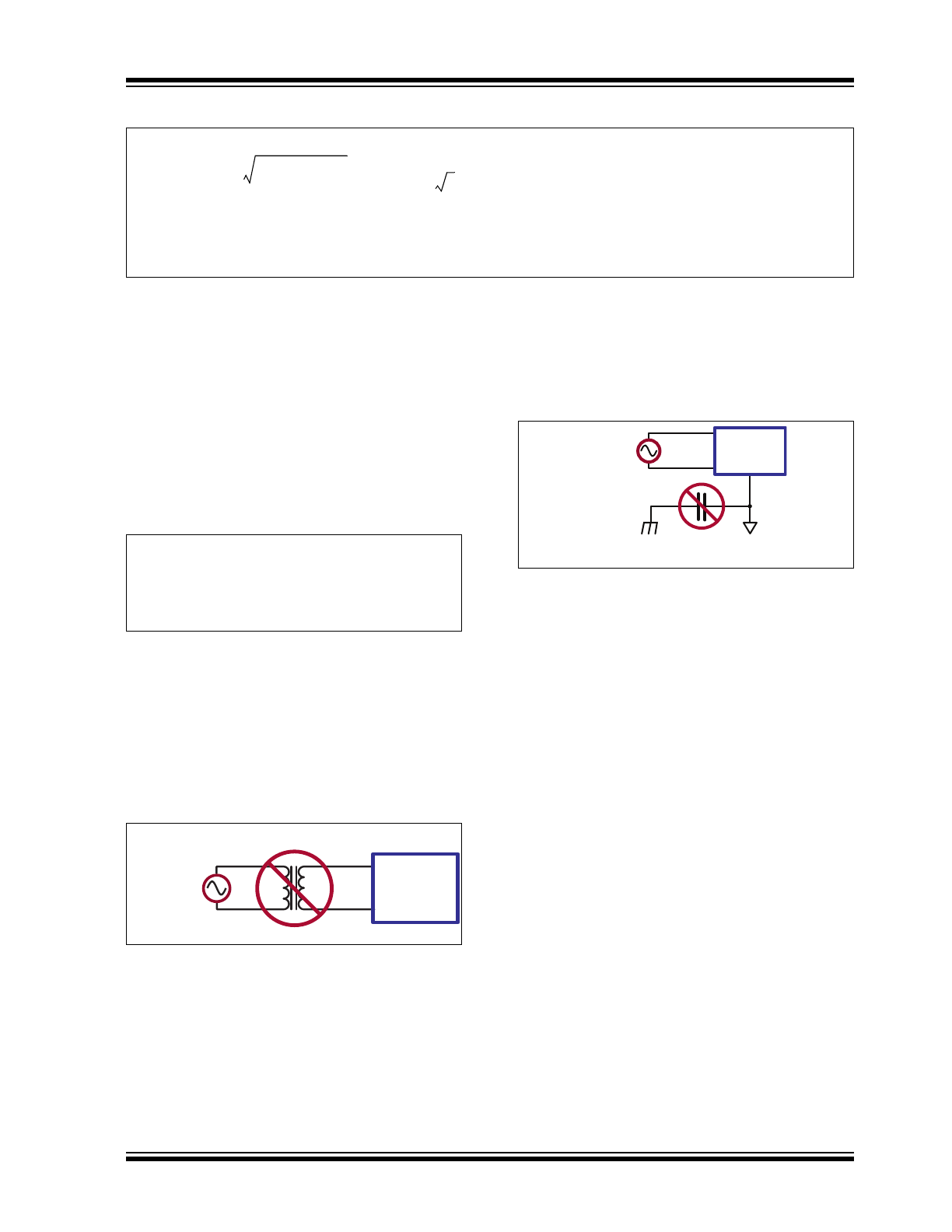
During initial testing, it is tempting to use an isolation
transformer or a variable transformer on the AC line.
However, the high inductance of the transformer
(frequently in mH range) should not be used because it
interferes with the normal operation of the
SR086/SR087. This is not a concern with the normal
inductance of the AC line or for AC line filters.
AC Line
SR086
Circuitry
FIGURE 3-3:
Line Transformer.
As shown in
Figure 3-3
, the SR086/SR087 draw
current from the AC line (in short, high current pulses).
The transformer’s high inductance tends to limit the
current pulse. Furthermore, inductive kickback on the
falling edge of the current pulse can create high voltage
spikes which must be absorbed by the transient
protector.
3.5
Electromagnetic Interference
(EMI) Capacitor
Small-value capacitors from circuit common to earth
ground should not be used as they prevent the
SR086/SR087 from operating. See
Figure 3-4
.
AC Line
SR086 &
Circuitry
earth
ground
circuit
common
FIGURE 3-4:
EMI Capacitor.
3.6
EMI
The SR086/SR087 circuits, as shown in the
Functional Block Diagrams
, meet FCC Class B and
CISPR 14-1 (household appliances) requirements for
conducted emissions for combined loads of less than
20 mA (I
OUT
+ I
REG
).
3.7
Fuse
Although the average current drawn from the AC line is
low, the RMS current is fairly high due to the current
being drawn in short high-current pulses. Since a fuse
is basically a resistor with a power dissipation given by
I
RMS
2
R, the fuse must be sized for the RMS current
and not the average current. For a 1W load at 120 VAC,
the RMS current is 700 mA
RMS
, while the RMS current
for a 0.5W load at 230 VAC is 360 mA
RMS
.
3.8
Load
Total load on the SR086/SR087 is the total load current
drawn from V
OUT
(I
OUT
), and since the linear regulator
is supplied from V
OUT
, it also includes the current
drawn from V
REG
(I
REG
). Total load is calculated in
Equation 3-6
and
Equation 3-7
.
SR086/SR087
DS20005544A-page 10
2017 Microchip Technology Inc.
EQUATION 3-6:
I
LOAD
I
OUT
I
REG
+
=
EQUATION 3-7:
P
LOAD
V
OUT
I
OUT
I
REG
+
=
3.9
Uninterruptible Power Supply
(UPS)
The SR086/SR087 will not operate from a UPS with a
square wave output. This type of output is usually
referred to as “modified sine wave.”
3.10
Transient Protection
The transient protector must be located before the
bridge rectifier. The reason for this is to minimize
capacitance to allow the rectified AC to fall below V
OUT
.
Since there is no capacitor to absorb AC line transients,
complete transient protection must be provided by the
TVS or MOV device. Since the recommended IGBT is
rated at 1.2 kV and the SR086/SR087 never see the full
input voltage, the bridge rectifier becomes the limiting
element when selecting an MOV. When using a 1 kV
bridge, an MOV having a clamping voltage of greater
than 1 kV is recommended.
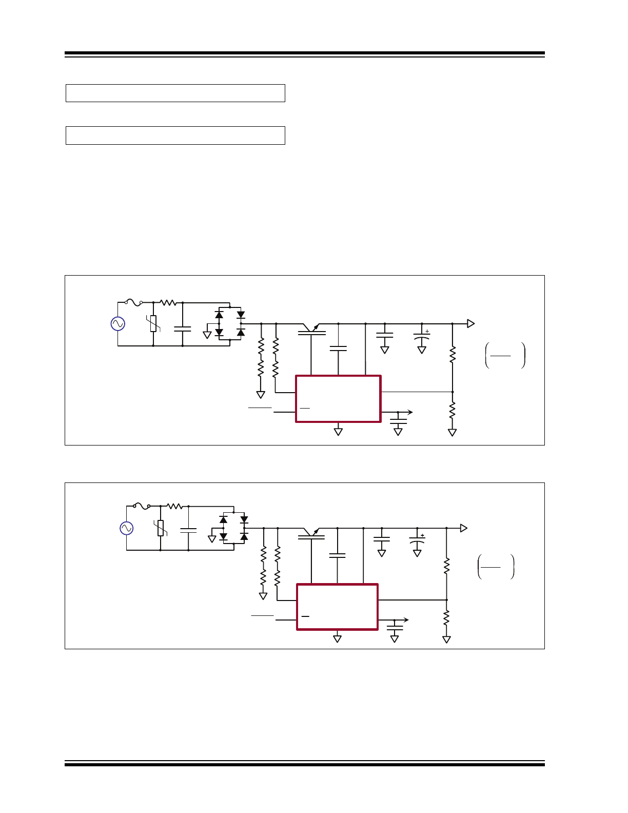
An RC network on the AC line, as shown in
Figure 3-5
and
Figure 3-6
, affords additional protection from line
transients as well as reducing conducted EMI. It does,
however, reduce power supply efficiency.
R
2
10.0k
Ω
1.0μF
1.0μF
240VAC
X2
1.0kV
1.0A
275V
50A
90 to
270VAC
50/60Hz
200kΩ
STGD5NB120SZ
V
OUT
- 1
1.25V
R
1
= R
2
3.3V
@60mA
100nF
GND
VREG
FB
VOUT
VGD
GATE
VIN
EN
Enable
1.0A
V
OUT
9.0 - 50VDC
@ 100mA - I
REG
SR086
100nF
10Ω, 3.0W
Wire Wound
470μF
200kΩ
510kΩ
510kΩ
FIGURE 3-5:
SR086 Additional Transient Protection.
R
2
10.0k
Ω
1.0μF
1.0μF
240VAC
X2
1.0kV
1.0A
275V
50A
90 to
270VAC
50/60Hz
200kΩ
STGD5NB120SZ
V
OUT
- 1
1.25V
R
1
= R
2
5.0V
@60mA
100nF
GND
VREG
FB
VOUT
VGD
GATE
VIN
EN
Enable
1.0A
V
OUT
9.0 - 50VDC
@ 100mA - I
REG
SR087
100nF
10Ω, 3.0W
Wire Wound
470μF
200kΩ
510kΩ
510kΩ
FIGURE 3-6:
SR087 Additional Transient Protection.