
2003 Microchip Technology Inc.
DS11195C-page 1
M
MCP41XXX/42XXX
Features
• 256 taps for each potentiometer
• Potentiometer values for 10 k
Ω, 50 kΩ and
100 k
Ω
• Single and dual versions
• SPI™ serial interface (mode 0,0 and 1,1)
• ±1 LSB max INL & DNL
• Low power CMOS technology
• 1 µA maximum supply current in static operation
• Multiple devices can be daisy-chained together
(MCP42XXX only)
• Shutdown feature open circuits of all resistors for
maximum power savings
• Hardware shutdown pin available on MCP42XXX
only
• Single supply operation (2.7V - 5.5V)
• Industrial temperature range: -40°C to +85°C
• Extended temperature range: -40°C to +125°C
Block Diagram
Description
The MCP41XXX and MCP42XXX devices are 256-
position, digital potentiometers available in 10 k
Ω,
50 k
Ω and 100 kΩ resistance versions. The
MCP41XXX is a single-channel device and is offered in
an 8-pin PDIP or SOIC package. The MCP42XXX con-
tains two independent channels in a 14-pin PDIP, SOIC
or TSSOP package. The wiper position of the
MCP41XXX/42XXX varies linearly and is controlled via
an industry-standard SPI interface. The devices con-
sume <1 µA during static operation. A software shut-
down feature is provided that disconnects the “A”
terminal from the resistor stack and simultaneously con-
nects the wiper to the “B” terminal. In addition, the dual
MCP42XXX has a SHDN pin that performs the same
function in hardware. During shutdown mode, the con-
tents of the wiper register can be changed and the
potentiometer returns from shutdown to the new value.
The wiper is reset to the mid-scale position (80h) upon
power-up. The RS (reset) pin implements a hardware
reset and also returns the wiper to mid-scale. The
MCP42XXX SPI interface includes both the SI and SO
pins, allowing daisy-chaining of multiple devices. Chan-
nel-to-channel resistance matching on the MCP42XXX
varies by less than 1%. These devices operate from a
single 2.7 - 5.5V supply and are specified over the
extended and industrial temperature ranges.
Package Types
16-Bit
Shift
V
DD
V
SS
SI
SCK
RS SHDN
PB1
PA1
PW1
Resistor
Array 1*
Wiper
Register
PB0
PW0
PA0
Resistor
Array 0
Wiper
Register
Register
S0
Control
Logic
CS
*Potentiometer P1 is only available on the dual
MCP42XXX version.
MCP42XXX
1
2
3
4
11
12
13
14
8
9
10
5
6
7
PDIP/SOIC/TSSOP
PB1
PA1
PW1
SHDN
SO
RS
PW0
PB0
CS
PA0
SCK
SI
V
SS
V
DD
M
C
P
4
1XXX
1
2
3
4
5
6
7
8
PDIP/SOIC
PB0
PA0
V
DD
PW0
V
SS
CS
SCK
SI
Single/Dual Digital Potentiometer with SPI
™
Interface
MCP41XXX/42XXX
DS11195C-page 2
2003 Microchip Technology Inc.
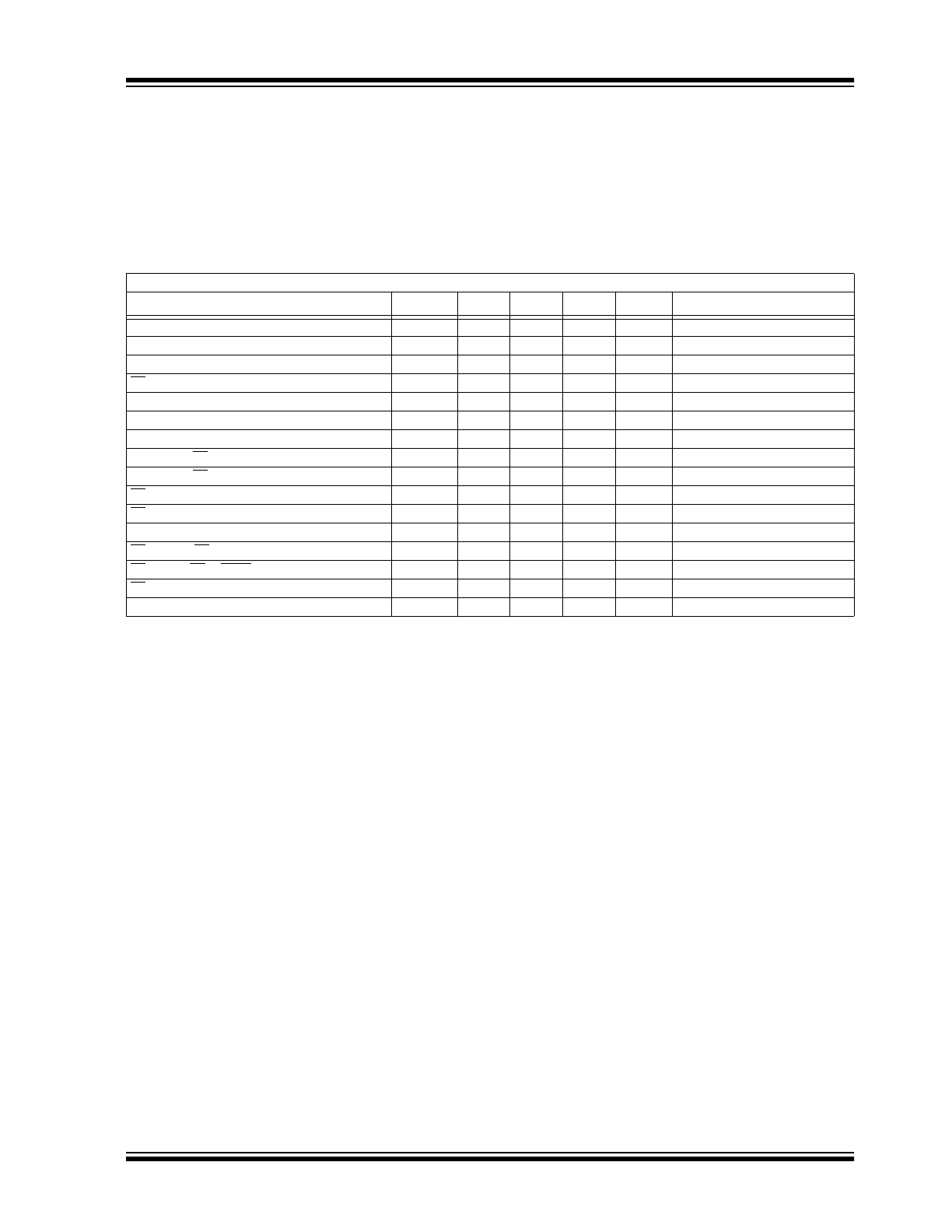
1.0
ELECTRICAL CHARACTERISTICS
DC CHARACTERISTICS: 10 k
Ω VERSION
Electrical Characteristics: Unless otherwise indicated, V
DD
= +2.7V to 5.5V, T
A
= -40°C to +85°C (TSSOP devices are only specified at +25°C and
+85°C). Typical specifications represent values for V
DD
= 5V, V
SS
= 0V, V
B
= 0V, T
A
= +25°C.
Parameters
Sym
Min
Typ
Max
Units
Conditions
Rheostat Mode
Nominal Resistance
R
8
10
12
k
Ω
T
A
= +25°C (Note 1)
Rheostat Differential Non Linearity
R-DNL
-1
±1/4
+1
LSB
Note 2
Rheostat Integral Non Linearity
R-INL
-1
±1/4
+1
LSB
Note 2
Rheostat Tempco
∆R
AB
/
∆T
—
800
—
ppm/°C
Wiper Resistance
R
W
—
52
100
Ω
V
DD
= 5.5V, I
W
= 1 mA, code 00h
R
W
—
73
125
Ω
V
DD
= 2.7V, I
W
= 1 mA, code 00h
Wiper Current
I
W
-1
—
+1
mA
Nominal Resistance Match
∆R/R
—
0.2
1
%
MCP42010 only, P0 to P1; T
A
= +25°C
Potentiometer Divider
Resolution
N
8
—
—
Bits
Monotonicity
N
8
—
—
Bits
Differential Non-Linearity
DNL
-1
±1/4
+1
LSB
Note 3
Integral Non-Linearity
INL
-1
±1/4
+1
LSB
Note 3
Voltage Divider Tempco
∆V
W
/
∆T
—
1
—
ppm/°C Code 80h
Full Scale Error
V
WFSE
-2
-0.7
0
LSB
Code FFh, V
DD
= 5V, see Figure 2-25
V
WFSE
-2
-0.7
0
LSB
Code FFh, V
DD
= 3V, see Figure 2-25
Zero Scale Error
V
WZSE
0
+0.7
+2
LSB
Code 00h, V
DD
= 5V, see Figure 2-25
V
WZSE
0
+0.7
+2
LSB
Code 00h, V
DD
= 3V, see Figure 2-25
Resistor Terminals
Voltage Range
V
A,B,W
0
—
V
DD
Note 4
Capacitance (C
A
or C
B
)
—
15
—
pF
f = 1 MHz, Code = 80h, see Figure 2-30
Capacitance
C
W
—
5.6
—
pF
f = 1 MHz, Code = 80h, see Figure 2-30
Dynamic Characteristics (All dynamic characteristics use V
DD
= 5V)
Bandwidth -3dB
BW
—
1
—
MHz
V
B
= 0V, Measured at Code 80h,
Output Load = 30
P
F
Settling Time
t
S
—
2
—
µS
V
A
= V
DD
,V
B
= 0V, ±1% Error Band, Transition
from Code 00h to Code 80h, Output Load = 30 pF
Resistor Noise Voltage
e
NWB
—
9
—
nV/
√Hz V
A
= Open, Code 80h
, f =1 kHz
Crosstalk
C
T
—
-95
—
dB
V
A
= V
DD
, V
B
= 0V (Note 5)
Digital Inputs/Outputs (CS, SCK, SI, SO) See Figure 2-12 for RS and SHDN pin operation
Schmitt Trigger High-Level Input Voltage
V
IH
0.7V
DD
—
—
V
Schmitt Trigger Low-Level Input Voltage
V
IL
—
—
0.3V
DD
V
Hysteresis of Schmitt Trigger Inputs
V
HYS
—
0.05V
DD
—
Low-Level Output Voltage
V
OL
—
—
0.40
V
I
OL
= 2.1 mA, V
DD
= 5V
High-Level Output Voltage
V
OH
V
DD
- 0.5
—
—
V
I
OH
= -400 µA, V
DD
= 5V
Input Leakage Current
I
LI
-1
—
+1
µA
CS = V
DD
, V
IN
= V
SS
or V
DD
, includes V
A
SHDN=0
Pin Capacitance (All inputs/outputs)
C
IN
, C
OUT
—
10
—
pF
V
DD
= 5.0V, T
A
= +25°C, f
c
= 1 MHz
Power Requirements
Operating Voltage Range
V
DD
2.7
—
5.5
V
Supply Current, Active
I
DDA
—
340
500
µA
V
DD
= 5.5V, CS = V
SS
, f
SCK
= 10 MHz,
SO = Open, Code FFh (Note 6)
Supply Current, Static
I
DDS
—
0.01
1
µA
CS, SHDN, RS = V
DD
= 5.5V, SO = Open (Note 6)
Power Supply Sensitivity
PSS
—
0.0015
0.0035
%/%
V
DD
= 4.5V - 5.5V, V
A
= 4.5V, Code 80h
PSS
—
0.0015
0.0035
%/%
V
DD
= 2.7V - 3.3V, V
A
= 2.7V, Code 80h
Note
1:
V
AB
= V
DD
, no connection on wiper.
2:
Rheostat position non-linearity R-INL is the deviation from an ideal value measured between the maximum resistance and the minimum
resistance wiper positions. R-DNL measures the relative step change from the ideal between successive tap positions. I
W
= 50 µA for
V
DD
= 3V and I
W
= 400 µA for V
DD
= 5V for 10 k
Ω version. See Figure 2-26 for test circuit.
3:
INL and DNL are measured at V
W
with the device configured in the voltage divider or potentiometer mode. V
A
= V
DD
and V
B
= 0V. DNL
specification limits of ±1 LSB max are specified monotonic operating conditions. See Figure 2-25 for test circuit.
4:
Resistor terminals A,B and W have no restrictions on polarity with respect to each other. Full-scale and zero-scale error were measured
using Figure 2-25.
5:
Measured at V
W
pin where the voltage on the adjacent V
W
pin is swinging full-scale.
6:
Supply current is independent of current through the potentiometers.
2003 Microchip Technology Inc.
DS11195C-page 3
MCP41XXX/42XXX
DC CHARACTERISTICS: 50 k
Ω VERSION
Electrical Characteristics: Unless otherwise indicated, V
DD
= +2.7V to 5.5V, T
A
= -40°C to +85°C (TSSOP devices are only specified at +25°C and
+85°C). Typical specifications represent values for V
DD
= 5V, V
SS
= 0V, V
B
= 0V, T
A
= +25°C.
Parameters
Sym
Min
Typ
Max
Units
Conditions
Rheostat Mode
Nominal Resistance
R
35
50
65
k
Ω
T
A
= +25°C (Note 1)
Rheostat Differential Non-Linearity
R-DNL
-1
±1/4
+1
LSB
Note 2
Rheostat Integral Non-Linearity
R-INL
-1
±1/4
+1
LSB
Note 2
Rheostat Tempco
∆R
AB
/
∆T
—
800
—
ppm/°C
Wiper Resistance
R
W
—
125
175
Ω
V
DD
= 5.5V, I
W
= 1 mA, code 00h
R
W
—
175
250
Ω
V
DD
= 2.7V, I
W
= 1 mA, code 00h
Wiper Current
I
W
-1
—
+1
mA
Nominal Resistance Match
∆R/R
—
0.2
1
%
MCP42050 only, P0 to P1;T
A
= +25°C
Potentiometer Divider
Resolution
N
8
—
—
Bits
Monotonicity
N
8
—
—
Bits
Differential Non-Linearity
DNL
-1
±1/4
+1
LSB
Note 3
Integral Non-Linearity
INL
-1
±1/4
+1
LSB
Note 3
Voltage Divider Tempco
∆V
W
/
∆T
—
1
—
ppm/°C Code 80h
Full-Scale Error
V
WFSE
-1
-0.25
0
LSB
Code FFh, V
DD
= 5V, see Figure 2-25
V
WFSE
-1
-0.35
0
LSB
Code FFh, V
DD
= 3V, see Figure 2-25
Zero-Scale Error
V
WZSE
0
+0.25
+1
LSB
Code 00h, V
DD
= 5V, see Figure 2-25
V
WZSE
0
+0.35
+1
LSB
Code 00h, V
DD
= 3V, see Figure 2-25
Resistor Terminals
Voltage Range
V
A,B,W
0
—
V
DD
Note 4
Capacitance (C
A
or C
B
)
—
11
—
pF
f =1 MHz, Code = 80h, see Figure 2-30
Capacitance
C
W
—
5.6
—
pF
f =1 MHz, Code = 80h, see Figure 2-30
Dynamic Characteristics (All dynamic characteristics use V
DD
= 5V)
Bandwidth -3dB
BW
—
280
—
MHz
V
B
= 0V, Measured at Code 80h,
Output Load = 30
P
F
Settling Time
t
S
—
8
—
µS
V
A
= V
DD
,V
B
= 0V, ±1% Error Band, Transition
from Code 00h to Code 80h, Output Load = 30 pF
Resistor Noise Voltage
e
NWB
—
20
—
nV/
√Hz V
A
= Open, Code 80h
, f =1 kHz
Crosstalk
C
T
—
-95
—
dB
V
A
= V
DD
, V
B
= 0V (Note 5)
Digital Inputs/Outputs (CS, SCK, SI, SO) See Figure 2-12 for RS and SHDN pin operation.
Schmitt Trigger High-Level Input Voltage
V
IH
0.7V
DD
—
—
V
Schmitt Trigger Low-Level Input Voltage
V
IL
—
—
0.3V
DD
V
Hysteresis of Schmitt Trigger Inputs
V
HYS
—
0.05V
DD
—
Low-Level Output Voltage
V
OL
—
—
0.40
V
I
OL
= 2.1 mA, V
DD
= 5V
High-Level Output Voltage
V
OH
V
DD
- 0.5
—
—
V
I
OH
= -400 µA, V
DD
= 5V
Input Leakage Current
I
LI
-1
—
+1
µA
CS = V
DD
, V
IN
= V
SS
or V
DD
, includes V
A
SHDN=0
Pin Capacitance (All inputs/outputs)
C
IN
, C
OUT
—
10
—
pF
V
DD
= 5.0V, T
A
= +25°C, f
c
= 1 MHz
Power Requirements
Operating Voltage Range
V
DD
2.7
—
5.5
V
Supply Current, Active
I
DDA
—
340
500
µA
V
DD
= 5.5V, CS = V
SS
, f
SCK
= 10 MHz,
SO = Open, Code FFh (Note 6)
Supply Current, Static
I
DDS
—
0.01
1
µA
CS, SHDN, RS = V
DD
= 5.5V, SO = Open (Note 6)
Power Supply Sensitivity
PSS
—
0.0015
0.0035
%/%
V
DD
= 4.5V - 5.5V, V
A
= 4.5V, Code 80h
PSS
—
0.0015
0.0035
%/%
V
DD
= 2.7V - 3.3V, V
A
= 2.7V, Code 80h
Note
1:
V
AB
= V
DD
, no connection on wiper.
2:
Rheostat position non-linearity R-INL is the deviation from an ideal value measured between the maximum resistance and the minimum
resistance wiper positions. R-DNL measures the relative step change from the ideal between successive tap positions. I
W
= V
DD
/R for
+3V or +5V for 50 k
Ω version. See Figure 2-26 for test circuit.
3:
INL and DNL are measured at V
W
with the device configured in the voltage divider or potentiometer mode. V
A
= V
DD
and V
B
= 0V. DNL
specification limits of ±1 LSB max are specified monotonic operating conditions. See Figure 2-25 for test circuit.
4:
Resistor terminals A,B and W have no restrictions on polarity with respect to each other. Full-scale and zero-scale error were measured
using Figure 2-25.
5:
Measured at V
W
pin where the voltage on the adjacent V
W
pin is swinging full scale.
6:
Supply current is independent of current through the potentiometers.
MCP41XXX/42XXX
DS11195C-page 4
2003 Microchip Technology Inc.
DC CHARACTERISTICS: 100 k
Ω VERSION
Electrical Characteristics: Unless otherwise indicated, V
DD
= +2.7V to 5.5V, T
A
= -40°C to +85°C (TSSOP devices are only specified at +25°C and
+85°C). Typical specifications represent values for V
DD
= 5V, V
SS
= 0V, V
B
= 0V, T
A
= +25°C.
Parameters
Sym
Min
Typ
Max
Units
Conditions
Rheostat Mode
Nominal Resistance
R
70
100
130
k
Ω
T
A
= +25°C (Note 1)
Rheostat Differential Non-Linearity
R-DNL
-1
±1/4
+1
LSB
Note 2
Rheostat Integral Non-Linearity
R-INL
-1
±1/4
+1
LSB
Note 2
Rheostat Tempco
∆R
AB
/
∆T
—
800
—
ppm/°C
Wiper Resistance
R
W
—
125
175
Ω
V
DD
= 5.5V, I
W
= 1 mA, code 00h
R
W
—
175
250
Ω
V
DD
= 2.7V, I
W
= 1 mA, code 00h
Wiper Current
I
W
-1
—
+1
mA
Nominal Resistance Match
∆R/R
—
0.2
1
%
MCP42010 only, P0 to P1;T
A
= +25°C
Potentiometer Divider
Resolution
N
8
—
—
Bits
Monotonicity
N
8
—
—
Bits
Differential Non-Linearity
DNL
-1
±1/4
+1
LSB
Note 3
Integral Non-Linearity
INL
-1
±1/4
+1
LSB
Note 3
Voltage Divider Tempco
∆V
W
/
∆T
—
1
—
ppm/°C Code 80h
Full-Scale Error
V
WFSE
-1
-0.25
0
LSB
Code FFh, V
DD
= 5V, see Figure 2-25
V
WFSE
-1
-0.35
0
LSB
Code FFh, V
DD
= 3V, see Figure 2-25
Zero-Scale Error
V
WZSE
0
+0.25
+1
LSB
Code 00h, V
DD
= 5V, see Figure 2-25
V
WZSE
0
+0.35
+1
LSB
Code 00h, V
DD
= 3V, see Figure 2-25
Resistor Terminals
Voltage Range
V
A,B,W
0
—
V
DD
Note 4
Capacitance (C
A
or C
B
)
—
11
—
pF
f =1 MHz, Code = 80h, see Figure 2-30
Capacitance
C
W
—
5.6
—
pF
f =1 MHz, Code = 80h, see Figure 2-30
Dynamic Characteristics (All dynamic characteristics use V
DD
= 5V.)
Bandwidth -3dB
BW
—
145
—
MHz
V
B
= 0V, Measured at Code 80h,
Output Load = 30
P
F
Settling Time
t
S
—
18
—
µS
V
A
= V
DD
,V
B
= 0V, ±1% Error Band, Transition
from Code 00h to Code 80h, Output Load = 30 pF
Resistor Noise Voltage
e
NWB
—
29
—
nV/
√Hz V
A
= Open, Code 80h
, f =1 kHz
Crosstalk
C
T
—
-95
—
dB
V
A
= V
DD
, V
B
= 0V (Note 5)
Digital Inputs/Outputs (CS, SCK, SI, SO) See Figure 2-12 for RS and SHDN pin operation.
Schmitt Trigger High-Level Input Voltage
V
IH
0.7V
DD
—
—
V
Schmitt Trigger Low-Level Input Voltage
V
IL
—
—
0.3V
DD
V
Hysteresis of Schmitt Trigger Inputs
V
HYS
—
0.05V
DD
—
Low-Level Output Voltage
V
OL
—
—
0.40
V
I
OL
= 2.1 mA, V
DD
= 5V
High-Level Output Voltage
V
OH
V
DD
- 0.5
—
—
V
I
OH
= -400 µA, V
DD
= 5V
Input Leakage Current
I
LI
-1
—
+1
µA
CS = V
DD
, V
IN
= V
SS
or V
DD
, includes V
A
SHDN=0
Pin Capacitance (All inputs/outputs)
C
IN
, C
OUT
—
10
—
pF
V
DD
= 5.0V, T
A
= +25°C, f
c
= 1 MHz
Power Requirements
Operating Voltage Range
V
DD
2.7
—
5.5
V
Supply Current, Active
I
DDA
—
340
500
µA
V
DD
= 5.5V, CS = V
SS
, f
SCK
= 10 MHz,
SO = Open, Code FFh (Note 6)
Supply Current, Static
I
DDS
—
0.01
1
µA
CS, SHDN, RS = V
DD
= 5.5V, SO = Open (Note 6)
Power Supply Sensitivity
PSS
—
0.0015
0.0035
%/%
V
DD
= 4.5V - 5.5V, V
A
= 4.5V, Code 80h
PSS
—
0.0015
0.0035
%/%
V
DD
= 2.7V - 3.3V, V
A
= 2.7V, Code 80h
Note
1:
V
AB
= V
DD
, no connection on wiper.
2:
Rheostat position non-linearity R-INL is the deviation from an ideal value measured between the maximum resistance and the minimum
resistance wiper positions. R-DNL measures the relative step change from the ideal between successive tap positions. I
W
= 50 µA for
V
DD
= 3V and I
W
= 400 µA for V
DD
= 5V for 10 k
Ω version. See Figure 2-26 for test circuit.
3:
INL and DNL are measured at V
W
with the device configured in the voltage divider or potentiometer mode. V
A
= V
DD
and V
B
= 0V. DNL
specification limits of ±1 LSB max are specified monotonic operating conditions. See Figure 2-25 for test circuit.
4:
Resistor terminals A,B and W have no restrictions on polarity with respect to each other. Full-scale and zero-scale error were measured
using Figure 2-25.
5:
Measured at V
W
pin where the voltage on the adjacent V
W
pin is swinging full-scale.
6:
Supply current is independent of current through the potentiometers.
2003 Microchip Technology Inc.
DS11195C-page 5
MCP41XXX/42XXX
Absolute Maximum Ratings †
V
DD
...................................................................................7.0V
All inputs and outputs w.r.t. V
SS
............... -0.6V to V
DD
+1.0V
Storage temperature .....................................-60°C to +150°C
Ambient temp. with power applied ................-60°C to +125°C
ESD protection on all pins
..................................................≥ 2 kV
† Notice: Stresses above those listed under “maximum rat-
ings” may cause permanent damage to the device. This is a
stress rating only and functional operation of the device at
those or any other conditions above those indicated in the
operational listings of this specification is not implied. Expo-
sure to maximum rating conditions for extended periods may
affect device reliability.
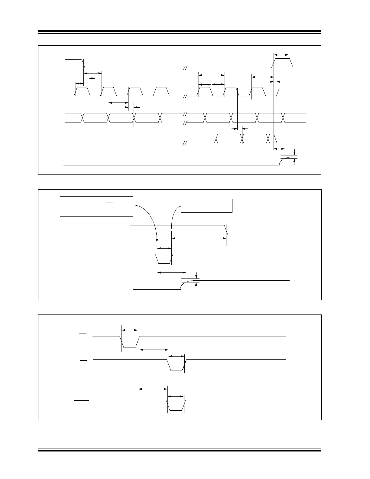
AC TIMING CHARACTERISTICS
Electrical Characteristics: Unless otherwise indicated, V
DD
= +2.7V to 5.5V, T
A
= -40°C to +85°C.
Parameter
Sym
Min.
Typ.
Max.
Units
Conditions
Clock Frequency
F
CLK
—
—
10
MHz
V
DD
= 5V (Note 1)
Clock High Time
t
HI
40
—
—
ns
Clock Low Time
t
LO
40
—
—
ns
CS Fall to First Rising CLK Edge
t
CSSR
40
—
—
ns
Data Input Setup Time
t
SU
40
—
—
ns
Data Input Hold Time
t
HD
10
—
—
ns
SCK Fall to SO Valid Propagation Delay
t
DO
—
80
ns
C
L
= 30 pF (Note 2)
SCK Rise to CS Rise Hold Time
t
CHS
30
—
—
ns
SCK Rise to CS Fall Delay
t
CS0
10
—
—
ns
CS Rise to CLK Rise Hold
t
CS1
100
—
—
ns
CS High Time
t
CSH
40
—
—
ns
Reset Pulse Width
t
RS
150
—
—
ns
Note 2
RS Rising to CS Falling Delay Time
t
RSCS
150
—
—
ns
Note 2
CS rising to RS or SHDN falling delay time
t
SE
40
—
—
ns
Note 3
CS low time
t
CSL
100
—
—
ns
Note 3
Shutdown Pulse Width
t
SH
150
—
—
ns
Note 3
Note
1:
When using the device in the daisy-chain configuration, maximum clock frequency is determined by a combination of propagation delay
time (t
DO
) and data input setup time (t
SU
). Max. clock frequency is therefore ~ 5.8 MHz based on SCK rise and fall times of 5 ns, t
HI
=
40 ns, t
DO
= 80 ns and t
SU
= 40 ns.
2:
Applies only to the MCP42XXX devices.
3:
Applies only when using hardware pins to exit software shutdown mode, MCP42XXX only.
MCP41XXX/42XXX
DS11195C-page 6
2003 Microchip Technology Inc.
FIGURE 1-1:
Detailed Serial interface Timing.
FIGURE 1-2:
Reset Timing.
FIGURE 1-3:
Software Shutdown Exit Timing.
CS
SCK
SI
msb in
t
SU
t
HD
t
CSSR
t
CSH
t
HI
t
LO
t
CSO
SO
t
CS1
1/F
CLK
t
CHS
t
DO
(First 16 bits out are always zeros)
V
OUT
±1%
±1% Error Band
t
S
RS
t
S
V
OUT
±1%
t
RS
±1% Error Band
CS
t
RSCS
Code 80h is latched
on rising edge of RS
Wiper position is changed to
mid-scale (80h) if RS is held
low for 150 ns
CS
t
CSL
RS
SHDN
t
SH
t
RS
t
SE
t
SE
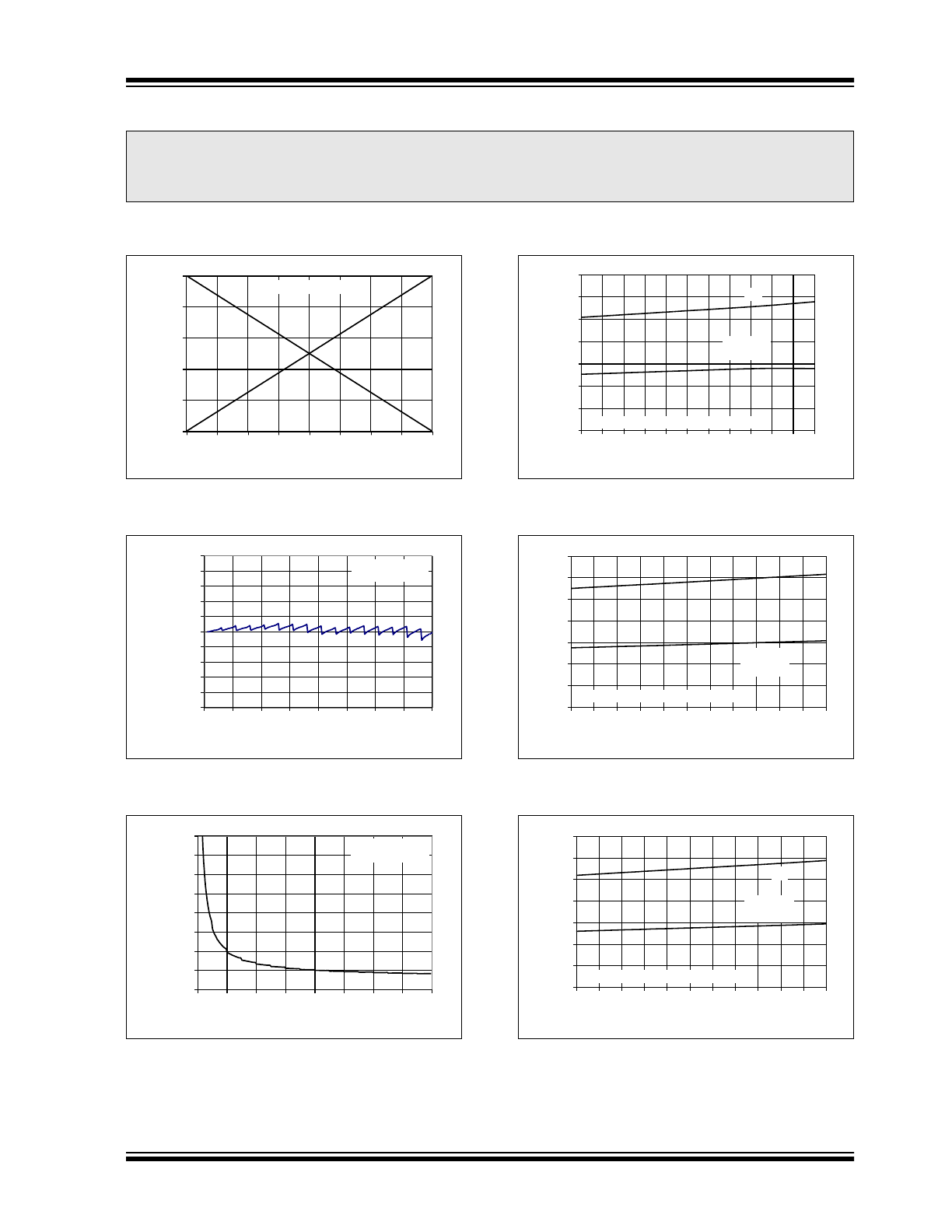
2003 Microchip Technology Inc.
DS11195C-page 7
MCP41XXX/42XXX
2.0
TYPICAL PERFORMANCE CURVES
Note: Unless otherwise indicated, curve represents 10 k
Ω, 50 kΩ and 100 kΩ devices, V
DD
= 5V, V
SS
= 0V, T
A
= +25°C,
V
B
= 0V.
FIGURE 2-1:
Normalized Wiper to End
Terminal Resistance vs. Code.
FIGURE 2-2:
Potentiometer INL Error vs.
Code.
FIGURE 2-3:
Potentiometer Mode
Tempco vs. Code.
FIGURE 2-4:
Nominal Resistance 10 k
Ω
vs. Temperature.
FIGURE 2-5:
Nominal Resistance 50 k
Ω
vs. Temperature.
FIGURE 2-6:
Nominal Resistance 100 k
Ω
vs. Temperature.
Note:
The graphs and tables provided following this note are a statistical summary based on a limited number of
samples and are provided for informational purposes only. The performance characteristics listed herein
are not tested or guaranteed. In some graphs or tables, the data presented may be outside the specified
operating range (e.g., outside specified power supply range) and therefore outside the warranted range.
0
0.2
0.4
0.6
0.8
1
0
32
64
96
128
160
192
224
256
Code (Decimal)
Normalized Resistance (
Ω
)
R
WB
R
WA
V
DD
= +3V to +5V
-0.5
-0.4
-0.3
-0.2
-0.1
0
0.1
0.2
0.3
0.4
0.5
0
32
64
96
128 160 192 224 256
Code (Decimal)
Potentiometer INL Error (LSB)
T
A
= -40°C to +85°C
Refer to Figure 2-25
-10
0
10
20
30
40
50
60
70
0
32
64
96
128 160 192 224 256
Code (Decimal)
Potentiometer Mode TempCo
(ppm / °C)
T
A
= -40°C to +85°C
V
A
= 3V
0
2
4
6
8
10
12
14
-40 -25 -10 5
20 35 50 65 80 95 110 125
Temperature (°C)
Nominal Resistance (k
Ω
)
R
AB
R
WB
Code = 80h
MCP41010, MCP42010 (10 k
Ω potentiometers)
0
10
20
30
40
50
60
70
-40 -25 -10
5
20 35 50 65 80 95 110 125
Temperature (°C)
Nominal Resistance (k
Ω
)
R
AB
R
WB
Code = 80h
MCP41050, MCP42050 (50 k
Ω potentiometers)
0
20
40
60
80
100
120
140
-40 -25 -10
5
20 35 50 65 80 95 110 125
Temperature (°C)
Nominal Resistance (k
Ω
)
MCP41100, MCP42100 (100 k
Ω potentiometers)
R
AB
R
WB
Code = 80h
MCP41XXX/42XXX
DS11195C-page 8
2003 Microchip Technology Inc.
Note: Unless otherwise indicated, curve represents 10 k
Ω, 50 kΩ and 100 kΩ devices, V
DD
= 5V, V
SS
= 0V, T
A
= +25°C,
V
B
= 0V.
FIGURE 2-7:
Rheostat INL Error vs.
Code.
FIGURE 2-8:
Rheostat Mode Tempco vs.
Code.
FIGURE 2-9:
Static Current vs.
Temperature.
FIGURE 2-10:
Active Supply Current vs.
Temperature.
FIGURE 2-11:
Active Supply Current vs.
Clock Frequency.
FIGURE 2-12:
Reset & Shutdown Pins
Current vs. Voltage.
-0.5
-0.4
-0.3
-0.2
-0.1
0
0.1
0.2
0.3
0.4
0.5
0
32
64
96
128
160
192
224
256
Code (Decimal)
Rheostat INL Error (LSB)
T
A
= +25°C
T
A
= +85°C
T
A
= -40°C
Refer to Figure 2-27
0
500
1000
1500
2000
2500
3000
0
32
64
96
128 160 192 224 256
Code (Decimal)
Rheostat Mode TempCo
(ppm / °C)
T
A
= -40°C to +85°C,
V
A
= no connect,
R
WB
measured
1
10
100
1000
-40 -25 -10 5 20 35 50 65 80 95 11
0
12
5
Temperature (°C)
Static Current (nA)
30
80
130
180
230
280
-40 -25 -10 5
20 35 50 65 80 95 110 125
Temperature (°C)
Active Supply Current (µA)
V
DD
= 5V
V
DD
= 3V
F
CLK
= 3 MHz
Code = FFh
0
100
200
300
400
500
600
700
800
900
1000
Clock Frequency (Hz)
Active Supply Current (mA)
A - V
DD
= 5.5V, Code = AAh
B - V
DD
= 3.3V, Code = AAh
C - V
DD
= 5.5V, Code = FFh
D - V
DD
= 3.3V, Code = FFh
A
B
C
D
1k
10k
100k
1M
10M
-7
-6
-5
-4
-3
-2
-1
0
1
0
2
4
6
RS & SHDN Pin Voltage (V)
RS & SHDN Sink Current (mA)
V
DD
= 5.5V
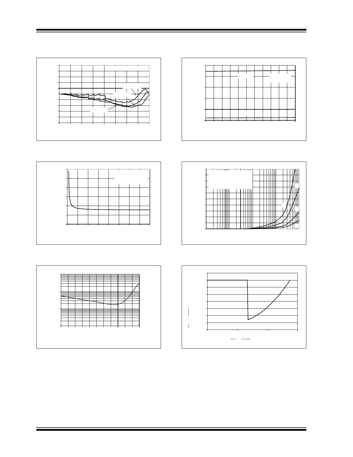
2003 Microchip Technology Inc.
DS11195C-page 9
MCP41XXX/42XXX
Note: Unless otherwise indicated, curve represents 10 k
Ω, 50 kΩ and 100 kΩ devices, V
DD
= 5V, V
SS
= 0V, T
A
= +25°C,
V
B
= 0V.
FIGURE 2-13:
10 k
Ω Device Wiper
Resistance Histogram.
FIGURE 2-14:
50 k
Ω, 100 kΩ Device Wiper
Resistance Histogram.
FIGURE 2-15:
One Position Settling Time.
FIGURE 2-16:
Full-Scale Settling Time.
FIGURE 2-17:
Digital Feed through vs.
Time.
FIGURE 2-18:
Gain vs. Frequency for
10 k
Ω Potentiometer.
0
20
40
60
80
100
120
140
160
180
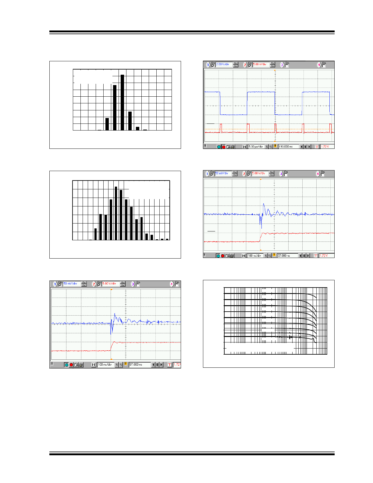
47 48 49 50 51 52 53 54 55 56 57 58 59
Wiper Resistance (
Ω)
Number of Occurrences
MCP41010,MCP42010
Code = 00h,
Sample Size = 400
0
20
40
60
80
100
120
140
115 117 119 121 123 125 127 129 131 133
Wiper Resistance (
Ω)
Number of Occurrences
MCP41050, MCP41100,
MCP42050, MCP42100
Code = 00h,
Sample Size = 796
V
OUT
Code = 7Fh
Code = 80h
CS
C
L
= 17 pF
V
OUT
00h
FFh
CS
C
L
= 27 pF
C
L
= 27 pF
Code = 80h
V
OUT
CS
-60
-54
-48
-42
-36
-30
-24
-18
-12
-6
0
6
Frequency (Hz)
Gain (dB)
C
L
= 30pF, Refer to Figure 2-29
MCP41010, MCP42010 (10k
Ω potentiometers)
Code = FFh
Code = 80h
Code = 40h
Code = 20h
Code = 10h
Code = 08h
Code = 04h
Code = 02h
Code = 01h
100
1k
10k
100k
1M
10M
MCP41XXX/42XXX
DS11195C-page 10
2003 Microchip Technology Inc.
Note: Unless otherwise indicated, curve represents 10 k
Ω, 50 kΩ and 100 kΩ devices, V
DD
= 5V, V
SS
= 0V, T
A
= +25°C,
V
B
= 0V.
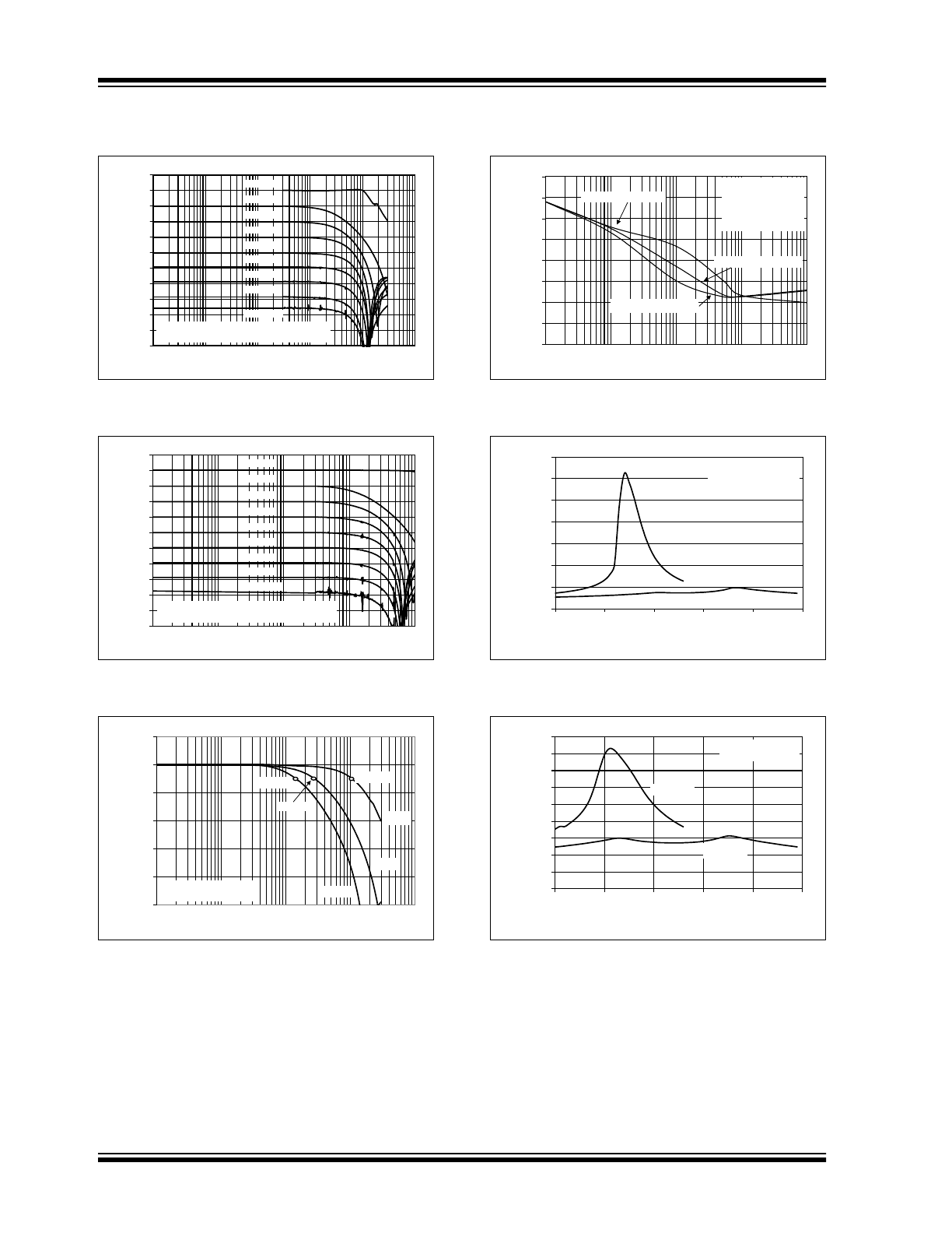
FIGURE 2-19:
Gain vs. Frequency for
50k
Ω Potentiometer.
FIGURE 2-20:
Gain vs. Frequency for
100k
Ω Potentiometer.
FIGURE 2-21:
-3 dB Bandwidths.
FIGURE 2-22:
Power Supply Rejection
Ratio vs. Frequency.
FIGURE 2-23:
10 k
Ω Wiper Resistance vs.
Voltage.
FIGURE 2-24:
50 k
Ω & 100 kΩ Wiper
Resistance vs. Voltage.
-60
-54
-48
-42
-36
-30
-24
-18
-12
-6
0
6
Frequency (Hz)
Gain (dB)
C
L
= 30pF, Refer to Figure 2-29
MCP41050, MCP42050 (50k
Ω potentiometers)
Code = FFh
Code = 80h
Code = 40h
Code = 20h
Code = 10h
Code = 08h
Code = 04h
Code = 02h
Code = 01h
100
1k
10k
100k
1M
10M
-60
-54
-48
-42
-36
-30
-24
-18
-12
-6
0
6
Frequency (Hz)
Gain (dB)
C
L
= 30pF, Refer to Figure 2-29
MCP41100, MCP42100 (100k
Ω potentiometers)
Code = FFh
Code = 80h
Code = 40h
Code = 20h
Code = 10h
Code = 08h
Code = 04h
Code = 02h
Code = 01h
100
1k
10k
100k
1M
-36
-30
-24
-18
-12
-6
0
Frequency (Hz)
Gain (dB)
279 kHz
145 kHz
1.06 MHz
10 k
Ω
50 k
Ω
100 k
Ω
C
L
= 30 pF, Code = 80h
Refer to Figure 2-29
1k
10k
100k
1M
10M
0
5
10
15
20
25
30
35
40
Frequency (Hz)
PSRR (dB)
100 k
Ω Potentiometer
50 k
Ω Potentiometer
10 k
Ω Potentiometer
V
DD
= 4.5V to 5.5V,
Code = 80h,
C
L
= 27 pF,
V
A
= 4V
Refer to Figure 2-28
1k
10k
100k
1M
10M
0
100
200
300
400
500
600
700
0
1
2
3
4
5
Terminal B Voltage (V)
Wiper Resistance (
Ω
)
MCP41010, MCP42010
Iw = 1 mA, Code = 00h,
Refer to Figure 2-27
V
DD
= 2.7V
V
DD
= 5V
0
50
100
150
200
250
300
350
400
450
0
1
2
3
4
5
Terminal B Voltage (V)
Wiper Resistance (
Ω
)
V
DD
= 2.7V
V
DD
= 5V
Code = 00h
Refer to Figure 2-27