
2002 Microchip Technology Inc.
DS21706A-page 1
M
MCP73828
Features
• Linear Charge Management Controller for Single
Lithium-Ion Cells
• High Accuracy Preset Voltage Regulation:
+1% (max)
• Two Preset Voltage Regulation Options:
- 4.1V - MCP73828-4.1
- 4.2V - MCP73828-4.2
• Programmable Charge Current
• Automatic Cell Preconditioning of Deeply
Depleted Cells, Minimizing Heat Dissipation
During Initial Charge Cycle
• Charge Complete Output CD10 for LED or
Microcontroller Interface
• Continuous Temperature Monitoring
• Automatic Power-Down when Input Power
Removed
• Temperature Range: -20°C to +85°C
• Packaging: 8-Pin MSOP
Applications
• Single Cell Lithium-Ion Battery Chargers
• Personal Data Assistants
• Cellular Telephones
• Hand Held Instruments
• Cradle Chargers
• Digital Cameras
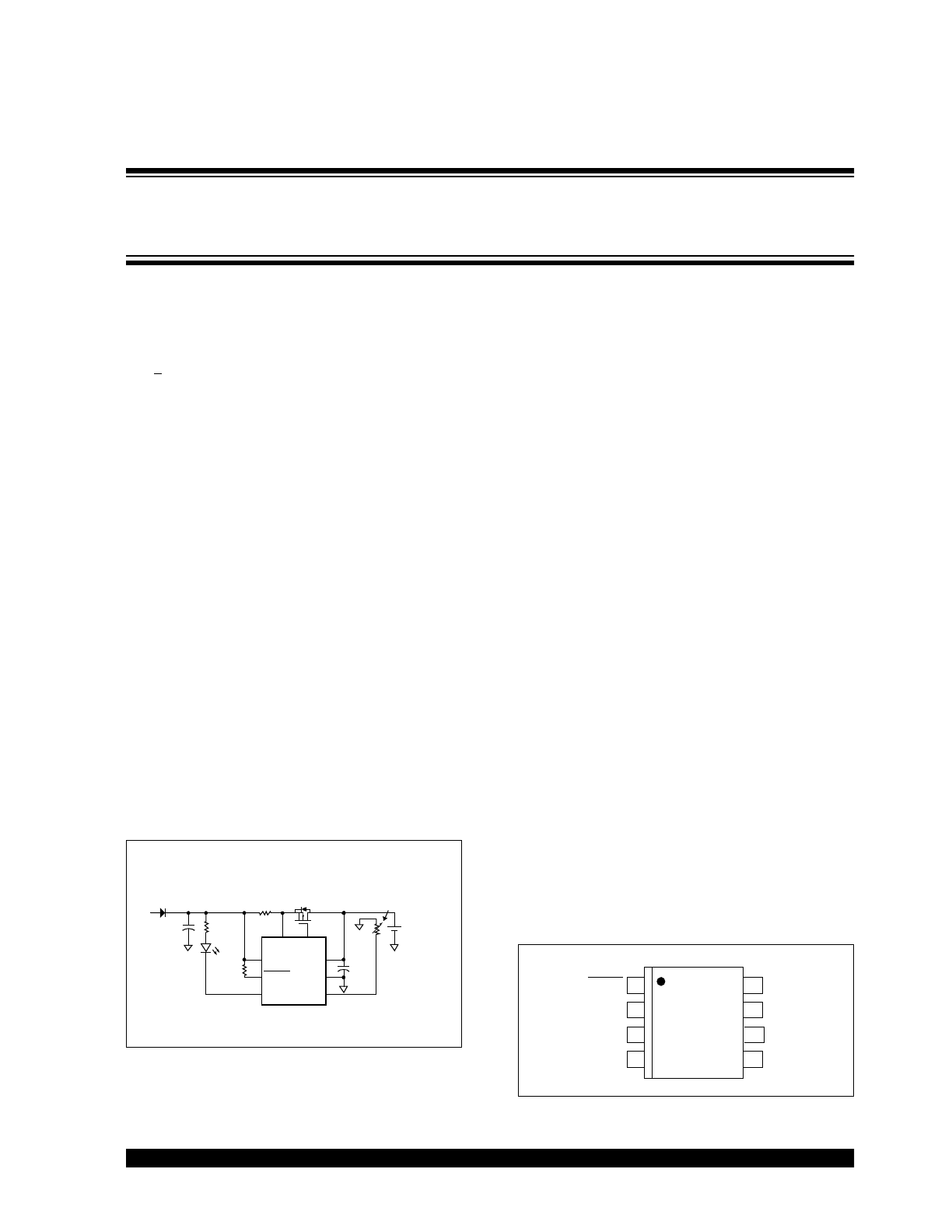
Typical Application Circuit
Description
The MCP73828 is a linear charge management con-
troller for use in space-limited, cost sensitive applica-
tions. The MCP73828 combines high accuracy
constant voltage, controlled current regulation, cell pre-
conditioning, cell temperature monitoring, and charge
complete indication in a space saving 8-pin MSOP
package. The MCP73828 provides a stand-alone
charge management solution.
The MCP73828 charges the battery in three phases:
preconditioning, controlled current, and constant volt-
age. If the battery voltage is below the internal low-volt-
age threshold, the battery is preconditioned with a
foldback current. The preconditioning phase protects
the lithium-ion cell and minimizes heat dissipation.
Following the preconditioning phase, the MCP73828
enters the controlled current phase. The MCP73828
allows for design flexibility with a programmable charge
current set by an external sense resistor. The charge
current is ramped up, based on the cell voltage, from
the foldback current to the peak charge current estab-
lished by the sense resistor. This phase is maintained
until the battery reaches the charge-regulation voltage.
Then, the MCP73828 enters the final phase, constant
voltage. The accuracy of the voltage regulation is better
than ±1% over the entire operating temperature range
and supply voltage range. The MCP73828-4.1 is preset
to a regulation voltage of 4.1V, while the MCP73828-
4.2 is preset to 4.2V. The charge complete output,
CD10, indicates when the charge current has dimin-
ished to approximately 10% of the peak charge current
established by the sense resistor.
The MCP73828 operates with an input voltage range
from 4.5V to 5.5V. The MCP73828 is fully specified
over the ambient temperature range of -20°C to +85°C.
Package Type
+
-
1
2
5
7
8
MCP73828
6
3
4
Thermistor
GND
V
DRV
V
SNS
V
IN
V
BAT
SHDN
10 µF
100 k
Ω
100 m
Ω
V
IN
Lithium-Ion
Cell
NDS8434
MA2Q705
5V
10 µF
Single
THERM
CD10
332
Ω
500 mA Lithium-Ion Battery Charger
MSOP
V
DRV
V
SNS
V
IN
V
BAT
SHDN 1
2
3
4
8
7
MCP73828
5
6
THERM
CD10
GND
Single Cell Lithium-Ion Charge Management Controller
with Charge Complete Indicator and Temperature Monitor

MCP73828
DS21706A-page 2
2002 Microchip Technology Inc.
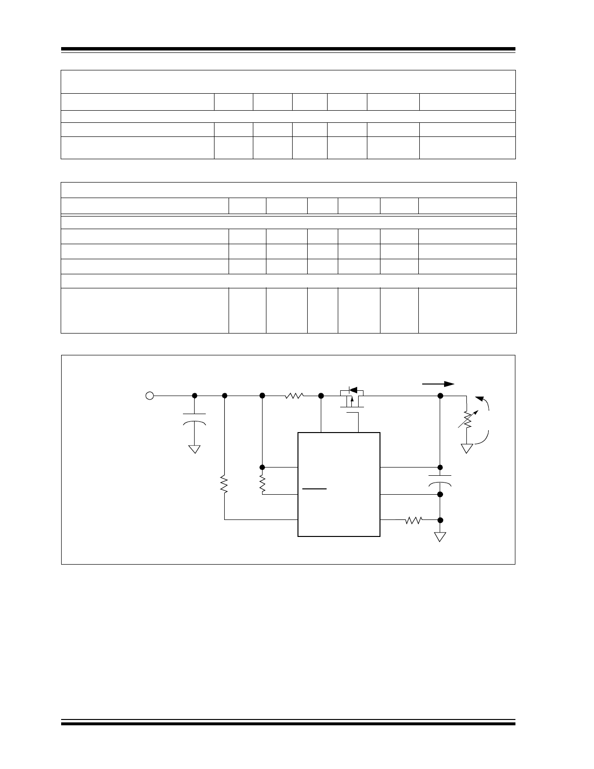
Functional Block Diagram
VO
LT
AG
E C
O
N
T
R
O
L
AMPL
IF
IE
R
SH
U
T
D
O
W
N
,
RE
F
E
RE
NC
E
G
E
NE
RA
T
O
R
V
RE
F
(
1
.2
V
)
+
–
V
RE
F
V
IN
CHA
R
G
E
CUR
RE
NT
CO
NT
RO
L A
M
P
L
IF
IE
R
+
–
V
REF
SH
D
N
V
BAT
GN
D
V
DRV
+
–
CH
A
R
G
E
CU
RRE
NT
AMPL
IF
IE
R
V
IN
V
SNS
1.
1
k
Ω
12
k
Ω
500
k
Ω
75
k
Ω
75
k
Ω
352.
5
k
Ω
(N
O
T
E 1
)
CH
A
R
G
E
CU
RRE
NT
F
O
LD
BAC
K AMP
LI
F
IE
R
+
–
37
.5
k
Ω
11
2
.5
k
Ω
V
IN
0.
3
V
C
LA
M
P
NO
T
E
1
: V
al
u
e =
340
.5K
Ω
F
or
MC
P
7
3828-
4.1
V
al
ue =
35
2.5K
Ω
F
or
MC
P
7
3828-
4.2
+
-
CH
A
R
G
E
CO
M
P
L
E
T
E
CO
M
P
A
R
A
T
O
R
CD1
0
+
–
CH
A
R
G
E
CO
M
P
L
E
T
E
AMPL
IF
IE
R
15
6
k
Ω
100
k
Ω
14
0
m
V
+
-
T
H
ER
MI
ST
O
R
VO
LT
AG
E
CO
M
P
A
R
A
T
O
R
S
+
-
83
9
m
V
11
3
m
V
V
REF
TH
E
R
M
V
IN
67
k
Ω
130
k
Ω
5k
Ω
21
k
Ω
140
m
V
I
TH
E
R
M
25
m
A
2002 Microchip Technology Inc.
DS21706A-page 3
MCP73828
1.0
ELECTRICAL
CHARACTERISTICS
1.1
Maximum Ratings*
V
IN
...................................................................... -0.3V to 6.0V
All inputs and outputs w.r.t. GND ................-0.3 to (V
IN
+0.3)V
Current at CD10 Pin ................................................ +/-30 mA
Current at V
DRV
.......................................................... +/-1 mA
Maximum Junction Temperature, T
J
.............................. 150°C
Storage temperature .....................................-65°C to +150°C
ESD protection on all pins
..................................................≥
4 kV
*Notice: Stresses above those listed under “Maximum Rat-
ings” may cause permanent damage to the device. This is a
stress rating only and functional operation of the device at
those or any other conditions above those indicated in the
operational listings of this specification is not implied. Expo-
sure to maximum rating conditions for extended periods may
affect device reliability.
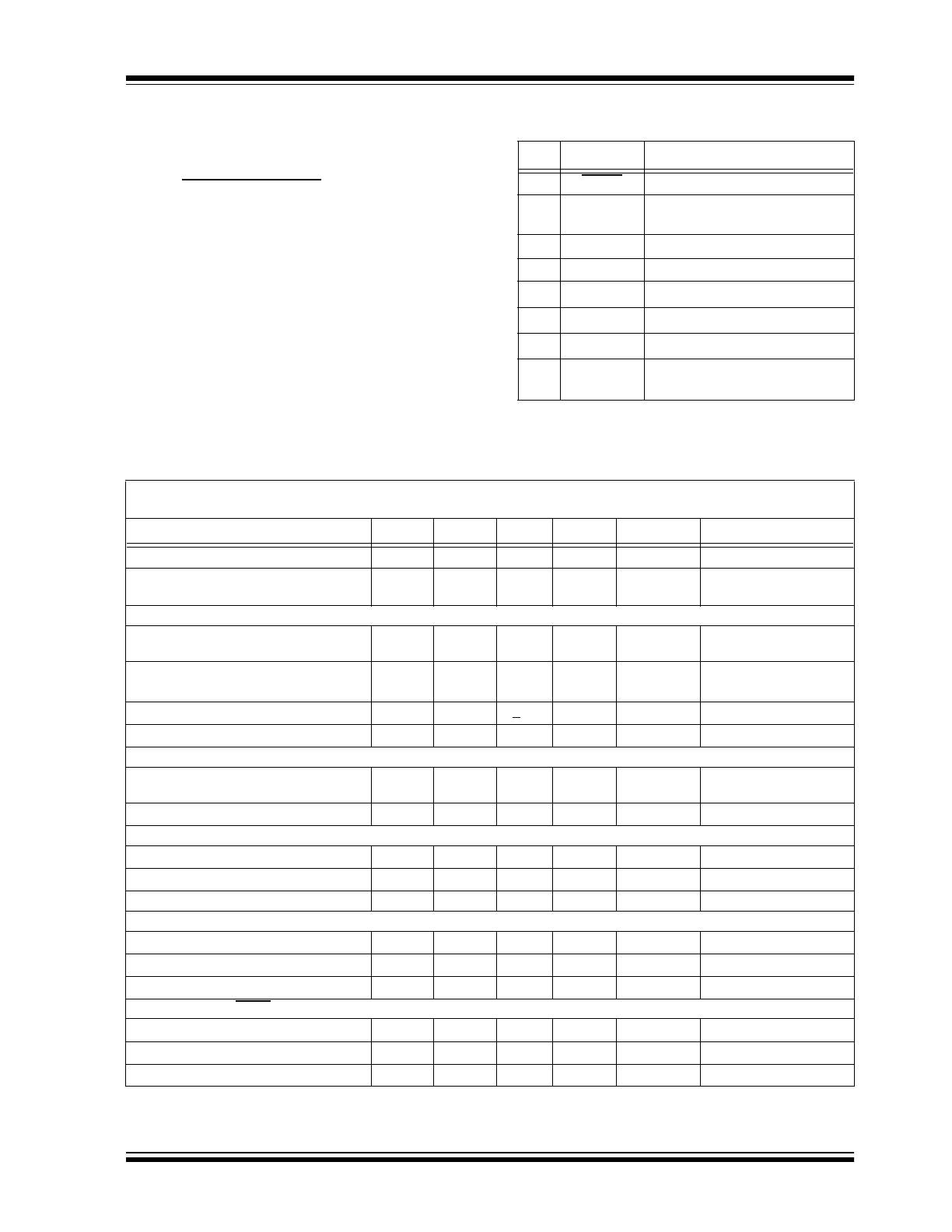
PIN FUNCTION TABLE
DC CHARACTERISTICS: MCP73828-4.1, MCP73828-4.2
Pin
Name
Description
1
SHDN
Logic Shutdown
2
GND
Battery Management
0V Reference
3
THERM
Cell Temperature Monitor
4
CD10
Charge Complete Output
5
V
BAT
Cell Voltage Monitor Input
6
V
DRV
Drive Output
7
V
SNS
Charge Current Sense Input
8
V
IN
Battery Management
Input Supply
Unless otherwise specified, all limits apply for V
IN
= [V
REG
(typ)+1V], R
SENSE
= 500 m
Ω,
T
A
= -20°C to +85°C.
Typical values are at +25°C. Refer to Figure 1-1 for test circuit.
Parameter
Sym
Min
Typ
Max
Units
Conditions
Supply Voltage
V
IN
4.5
—
5.5
V
Supply Current
I
IN
—
—
0.7
265
15
560
µA
Shutdown, V
SHDN
= 0V
Constant Voltage Mode
Voltage Regulation (Constant Voltage Mode)
Regulated Output Voltage
V
REG
4.059
4.158
4.1
4.2
4.141
4.242
V
V
MCP73828-4.1 only
MCP73828-4.2 only
Line Regulation
∆
V
BAT
-10
—
10
mV
V
IN
= 4.5V to 5.5V,
I
OUT
= 75 mA
Load Regulation
∆
V
BAT
-1
+0.2
+1
mV
I
OUT
=10 mA to 75 mA
Output Reverse Leakage Current
I
LK
—
10
—
µA
V
IN
=Floating, V
BAT
=V
REG
External MOSFET Gate Drive
Gate Drive Current
I
DRV
—
0.08
—
—
1
—
mA
mA
Sink, CV Mode
Source, CV Mode
Gate Drive Minimum Voltage
V
DRV
—
1.6
—
V
Current Regulation (Controlled Current Mode)
Current Sense Gain
A
CS
—
100
—
dB
∆
(V
SNS
-V
DRV
) /
∆
V
BAT
Current Limit Threshold
V
CS
40
53
75
mV
(V
IN
-V
SNS
) at I
OUT
Foldback Current Scale Factor
K
—
0.43
—
A/A
Charge Complete Indicator - CD10
Current Threshold
I
TH
—
10
—
%I
OUT(PEAK)
Low Output Voltage
V
OL
—
—
400
mV
I
SINK
= 10 mA
Leakage Current
I
LK
—
—
1
µA
I
SINK
=0 mA, V
CD10
=5.5V
Shutdown Input - SHDN
Input High Voltage Level
V
IH
40
—
—
%V
IN
Input Low Voltage Level
V
IL
—
—
25
%V
IN
Input Leakage Current
I
LK
—
—
1
µA
V
SHDN
= 0V to 5.5V
MCP73828
DS21706A-page 4
2002 Microchip Technology Inc.
TEMPERATURE SPECIFICATIONS
FIGURE 1-1:
MCP73828 Test Circuit.
Temperature Monitor - THERM
Thermistor Bias Current
I
THERM
22.5
25.0
27.5
µA
THERM Threshold Voltages
V
TH
—
—
113
839
—
—
mV
Lower Threshold Voltage
Upper Threshold Voltage
Unless otherwise specified, all limits apply for V
IN
= [V
REG
(typ)+1V], R
SENSE
= 500 m
Ω,
T
A
= -20°C to +85°C.
Typical values are at +25°C. Refer to Figure 1-1 for test circuit.
Parameter
Sym
Min
Typ
Max
Units
Conditions
Unless otherwise specified, all limits apply for V
IN
= 4.5V-5.5V
Parameters
Sym
Min
Typ
Max
Units
Conditions
Temperature Ranges
Specified Temperature Range
T
A
-20
—
+85
°C
Operating Temperature Range
T
A
-40
—
+125
°C
Storage Temperature Range
T
A
-65
—
+150
°C
Package Thermal Resistance
Thermal Resistance, 8L-MSOP
θ
JA
—
206
—
°C/W
Single Layer SEMI
G42-88 Standard
Board, Natural Convec-
tion
GND
V
DRV
V
SNS
V
IN
V
BAT
SHDN
1
2
5
7
8
6
100 k
Ω
R
SENSE
NDS8434
MCP73828
CD10
100 k
Ω
4
3
THERM
10 k
Ω
22 µF
22 µF
V
IN
= 5.1V
I
OUT
V
OUT
(MCP73828-4.1)
V
IN
= 5.2V
(MCP73828-4.2)
2002 Microchip Technology Inc.
DS21706A-page 5
MCP73828
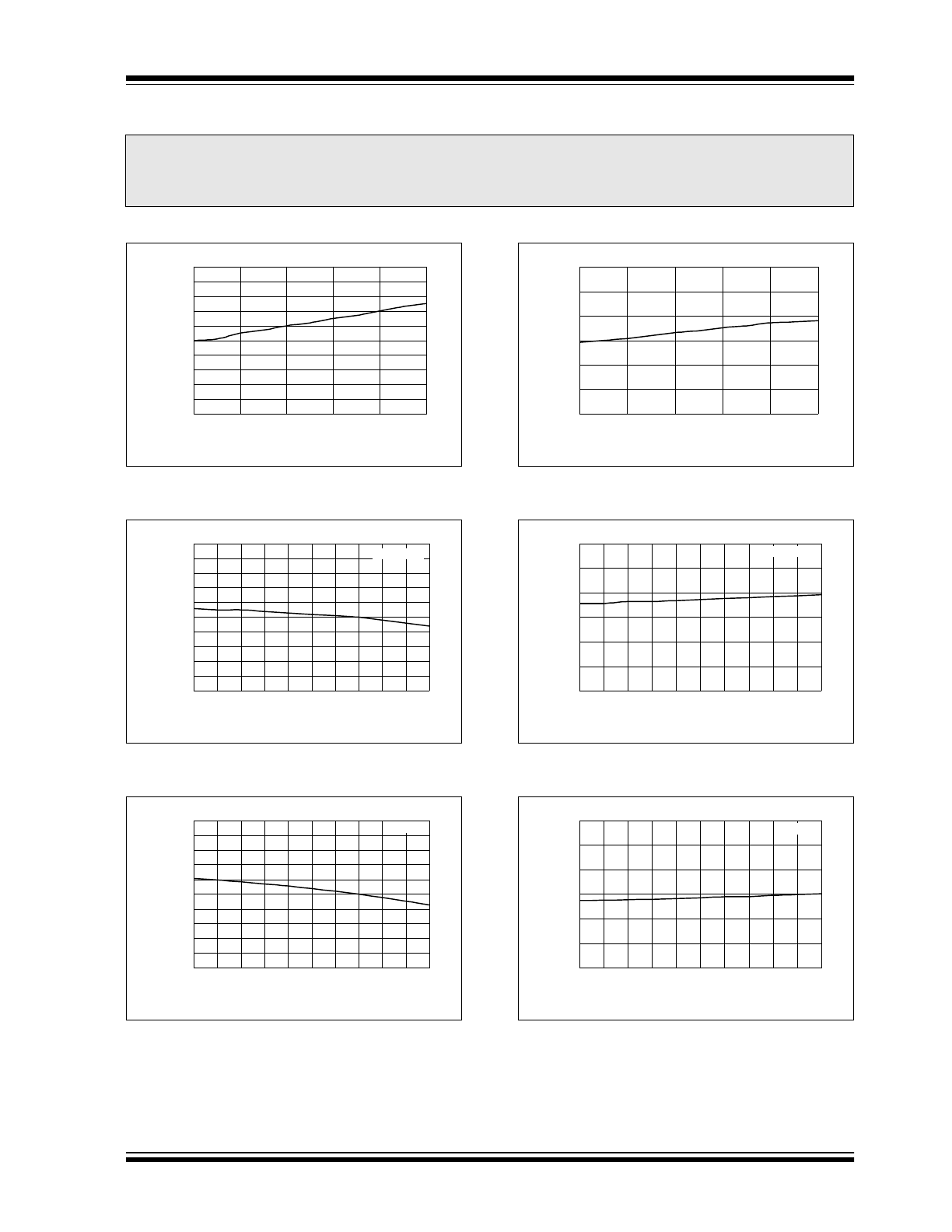
2.0
TYPICAL PERFORMANCE CHARACTERISTICS
Note: Unless otherwise indicated, I
OUT
= 10 mA, Constant Voltage Mode, T
A
=25°C. Refer to Figure 1-1 for test circuit.
FIGURE 2-1:
Output Voltage vs. Output Current
(MCP73828-4.2).
FIGURE 2-2:
Output Voltage vs. Input Voltage
(MCP73828-4.2).
FIGURE 2-3:
Output Voltage vs. Input Voltage
(MCP73828-4.2).
FIGURE 2-4:
Supply Current vs. Output Current.
FIGURE 2-5:
Supply Current vs. Input Voltage.
FIGURE 2-6:
Supply Current vs. Input Voltage.
Note:
The graphs and tables provided following this note are a statistical summary based on a limited number of
samples and are provided for informational purposes only. The performance characteristics listed herein
are not tested or guaranteed. In some graphs or tables, the data presented may be outside the specified
operating range (e.g., outside specified power supply range) and therefore outside the warranted range.
4.195
4.196
4.197
4.198
4.199
4.200
4.201
4.202
4.203
4.204
4.205
0
200
400
600
800
1000
Output Current (mA)
Output Voltage (V)
4.195
4.196
4.197
4.198
4.199
4.200
4.201
4.202
4.203
4.204
4.205
4.5
4.6
4.7
4.8
4.9
5.0
5.1
5.2
5.3
5.4
5.5
Input Voltage (V)
Output Voltage (V)
I
OUT
= 1000 mA
4.195
4.196
4.197
4.198
4.199
4.200
4.201
4.202
4.203
4.204
4.205
4.5
4.6
4.7
4.8
4.9
5.0
5.1
5.2
5.3
5.4
5.5
Input Voltage (V)
Output Voltage (V)
I
OUT
= 10 mA
200
225
250
275
300
325
350
0
200
400
600
800
1000
Output Current (mA)
Supply Current (
µ
A)
200
225
250
275
300
325
350
4.5
4.6
4.7
4.8
4.9
5.0
5.1
5.2
5.3
5.4
5.5
Input Voltage (V)
Supply Current (
µ
A)
I
OUT
= 1000 mA
200
225
250
275
300
325
350
4.5
4.6
4.7
4.8
4.9
5.0
5.1
5.2
5.3
5.4
5.5
Input Voltage (V)
Supply Current (
µ
A)
I
OUT
= 10 mA
MCP73828
DS21706A-page 6
2002 Microchip Technology Inc.
Note: Unless otherwise indicated, I
OUT
= 10 mA, Constant Voltage Mode, T
A
=25°C. Refer to Figure 1-1 for test circuit.
FIGURE 2-7:
Output Reverse Leakage Current vs.
Output Voltage.
FIGURE 2-8:
Output Reverse Leakage Current vs.
Output Voltage.
FIGURE 2-9:
Current Limit Foldback.
FIGURE 2-10: Supply Current vs. Temperature.
FIGURE 2-11: Output Voltage vs. Temperature
(MCP73828-4.2).
FIGURE 2-12: Power-Up / Power-Down.
0
2
4
6
8
10
12
14
16
2.0
2.5
3.0
3.5
4.0
4.5
Output Voltage (V)
Ouput Reverse Leakage Current (
µ
A)
85
o
C
25
o
C
-20
o
C
V
IN
= Floating
V
SHDN
= V
OUT
0.0
0.2
0.4
0.6
0.8
1.0
1.2
1.4
1.6
2.0
2.5
3.0
3.5
4.0
4.5
Output Voltage (V)
Output Reverse Leakage Current (
µ
A)
85
o
C
25
o
C
-20
o
C
V
IN
= Floating
V
SHDN
= GND
0.000
0.500
1.000
1.500
2.000
2.500
3.000
3.500
4.000
4.500
0
20
40
60
80
100
120
Output Current (mA)
Output Voltage (V)
200
225
250
275
300
325
350
-20
-10
0
10
20
30
40
50
60
70
80
Temperature (
o
C)
Supply Current (
µ
A)
4.190
4.192
4.194
4.196
4.198
4.200
4.202
4.204
4.206
-20
-10
0
10
20
30
40
50
60
70
80
Temperature (
o
C)
Output Voltage (V)
0.0
0.5
1.0
1.5
2.0
2.5
3.0
3.5
4.0
4.5
0
1
2
3
4
5
6
7
8
9
10
Input Voltage (V)
Output Voltage (V)
Power Up
Power Down
4
3
2
1
0
2002 Microchip Technology Inc.
DS21706A-page 7
MCP73828
Note: Unless otherwise indicated, I
OUT
= 10 mA, Constant Voltage Mode, T
A
=25°C. Refer to Figure 1-1 for test circuit.
FIGURE 2-13: Line Transient Response.
FIGURE 2-14: Line Transient Response.
FIGURE 2-15: Load Transient Response.
FIGURE 2-16: Load Transient Response.
MCP73828
DS21706A-page 8
2002 Microchip Technology Inc.
3.0
PIN DESCRIPTION
The descriptions of the pins are listed in Table 3-1.
TABLE 3-1:
Pin Function Table.
3.1
Logic Shutdown (SHDN)
Input to force charge termination, initiate charge, or ini-
tiate recharge.
3.2
Battery Management 0V Reference
(GND)
Connect to negative terminal of battery.
3.3
Cell Temperature Monitor (THERM)
Charging is inhibited when the input is outside the
upper and lower threshold limits. Connection of a
10 k
Ω
resistor between THERM and GND disables the
function when cell temperature monitoring is not
required.
3.4
Charge Complete Output (CD10)
Open-drain drive for connection to an LED for charge
complete indication. Alternatively, a pull-up resistor can
be applied for interfacing to a microcontroller. A low
impedance state indicates charging. A high impedance
indicates that the charge current has diminished below
10% of the peak charge current.
3.5
Cell Voltage Monitor Input (V
BAT
)
Voltage sense input. Connect to positive terminal of
battery. Bypass to GND with a minimum of 10 µF to
ensure loop stability when the battery is disconnected.
A precision internal resistor divider regulates the final
voltage on this pin to V
REG
.
3.6
Drive Output (V
DRV
)
Direct output drive of an external P-channel MOSFET
pass transistor for current and voltage regulation.
3.7
Charge Current Sense Input V
SNS
)
Charge current is sensed via the voltage developed
across an external precision sense resistor. The sense
resistor must be placed between the supply voltage
(V
IN
) and the source of the external pass transistor. A
50 m
Ω
sense resistor produces a fast charge current of
1 A, typically.
3.8
Battery Management Input Supply
(V
IN
)
A supply voltage of 4.5V to 5.5V is recommended.
Bypass to GND with a minimum of 10 µF.
Pin
Name
Description
1
SHDN
Logic Shutdown
2
GND
Battery Management
0V Reference
3
THERM
Cell Temperature Monitor
4
CD10
Charge Complete Output
5
V
BAT
Cell Voltage Monitor Input
6
V
DRV
Drive Output
7
V
SNS
Charge Current Sense Input
8
V
IN
Battery Management
Input Supply

2002 Microchip Technology Inc.
DS21706A-page 9
MCP73828
4.0
DEVICE OVERVIEW
The MCP73828 is a linear charge management con-
troller. Refer to the functional block diagram on page 2
and the typical application circuit, Figure 6-1.
4.1
Charge Qualification and
Preconditioning
Upon insertion of a battery or application of an external
supply, the MCP73828 automatically performs a series
of safety checks to qualify the charge. The SHDN pin
must be above the logic high level, and the cell temper-
ature monitor must be within the upper and lower
threshold limits. The qualification parameters are con-
tinuously monitored. Deviation beyond the limits, auto-
matically suspends the charge cycle.
After the qualification parameters have been met, the
MCP73828 initiates a charge cycle. The charge com-
plete output, CD10, is pulled low throughout the pre-
conditioning and controlled current phases (see
Table 5-1 for charge complete outputs). If the cell volt-
age is below the preconditioning threshold, 2.4V typi-
cally, the MCP73828 preconditions the cell with a
scaled back current. The preconditioning current is set
to approximately 43% of the fast charge peak current.
The preconditioning safely replenishes deeply
depleted cells and minimizes heat dissipation in the
external pass transistor during the initial charge cycle.
4.2
Controlled Current Regulation - Fast
Charge
Preconditioning ends and fast charging begins when
the cell voltage exceeds the preconditioning threshold.
Fast charge utilizes a foldback current scheme based
on the voltage at the V
SNS
input developed by the drop
across an external sense resistor, R
SENSE
, and the out-
put voltage, V
BAT
. Fast charge continues until the cell
voltage reaches the regulation voltage, V
REG
.
4.3
Constant Voltage Regulation
When the cell voltage reaches the regulation voltage,
V
REG
, constant voltage regulation begins. The
MCP73828 monitors the cell voltage at the V
OUT
pin.
This input is tied directly to the positive terminal of the
battery. The MCP73828 is offered in two fixed-voltage
versions for battery packs with either coke or graphite
anodes: 4.1V (MCP73828-4.1) and 4.2V
(MCP73828-4.2).
4.4
Charge Cycle Completion
The charge cycle can be terminated by a host micro-
controller when the charge current has diminished
below approximately 10% of the peak output voltage
level. The charge complete output will go to a high
impedance state signaling when the charge can be ter-
minated. The charge is terminated by pulling the shut-
down pin, SHDN, to a logic Low level.
MCP73828
DS21706A-page 10
2002 Microchip Technology Inc.
5.0
DETAILED DESCRIPTION
Refer to the typical application circuit, Figure 6-1.
5.1
Analog Circuitry
5.1.1
CELL TEMPERATURE MONITOR (THERM)
The cell temperature monitor, THERM, input is used to
inhibit charging when the battery temperature exceeds
a predetermined temperature range. This temperature
range is programmed externally with either a single
Thermistor or a resistor/Thermistor network. An exam-
ple of this type of network is illustrated in Figure 6-1.
The MCP73828 internally generates a current source
out of the THERM pin (shown in the Functional Block
Diagram). The nominal value of the current source
(I
THERM
) is 25 µA. This current flows through the ther-
mistor network to ground. The factory programmed
voltage range of the THERM input (V
TH
) is 113 mV
(typ) to 839 mV (typ). Dependent on the type of Ther-
mistor used and the resistive network, the temperature
trip points can be controlled. If the THERM pin is lower
that 113 mV or higher than 839 mV the device will shut-
down operation. This condition can be corrected by
bringing the THERM pin back between these threshold
voltages.
As an application example, if a 10 k
Ω
NTC Thermistor
with a sensitivity index (b) of 3982 is connected from
THERM to ground, the operational temperature range
is from –0.5°C to 44.2°C. See Section 6.1.1.6 for more
details concerning using the resistive network.
Alternatively, a positive temperature coefficient, PTC,
thermistor can be utilized. Connect the thermistor from
the THERM input to GND. If temperature monitoring is
not required, replace the thermistor with a standard
10 k
Ω
resistor.
5.1.2
CELL VOLTAGE MONITOR INPUT (V
BAT
)
The MCP73828 monitors the cell voltage at the V
BAT
pin. This input is tied directly to the positive terminal of
the battery. The MCP73828 is offered in two fixed-volt-
age versions for single cells with either coke or graphite
anodes: 4.1V (MCP73828-4.1) and 4.2V
(MCP73828-4.2).
5.1.3
GATE DRIVE OUTPUT (V
DRV
)
The MCP73828 controls the gate drive to an external
P-channel MOSFET, Q1. The P-channel MOSFET is
controlled in the linear region, regulating current and
voltage supplied to the cell. The drive output is auto-
matically turned off when the input supply falls below
the voltage sensed on the V
BAT
input.
5.1.4
CURRENT SENSE INPUT (V
SNS
)
Fast charge current regulation is maintained by the
voltage drop developed across an external sense resis-
tor, R
SENSE
, applied to the V
SNS
input pin. The follow-
ing formula calculates the value for R
SENSE
:
Where:
V
CS
is the current limit threshold.
I
OUT
is the desired peak fast charge current in
amps. The preconditioning current is scaled to
approximately 43% of I
OUT
.
5.1.5
SUPPLY VOLTAGE (V
IN
)
The V
IN
input is the input supply to the MCP73828. The
MCP73828 automatically enters a power-down mode if
the voltage on the V
IN
input falls below the voltage on
the V
BAT
pin. This feature prevents draining the battery
pack when the V
IN
supply is not present.
5.2
Digital Circuitry
5.2.1
SHUTDOWN INPUT (SHDN)
The shutdown input pin, SHDN, can be used to termi-
nate a charge anytime during the charge cycle, initiate
a charge cycle, or initiate a recharge cycle.
Applying a logic High input signal to the SHDN pin, or
tying it to the input source, enables the device. Apply-
ing a logic Low input signal disables the device and ter-
minates a charge cycle. In shutdown mode, the
device’s supply current is reduced to 0.7 µA, typically.
5.2.2
CHARGE COMPLETE OUTPUT (CD10)
A charge complete indicator, CD10, provides informa-
tion on the state of charge. The open-drain output can
be used to illuminate an external LED. Optionally, a
pull-up resistor can be used on the output for commu-
nication with a microcontroller. Table 5-1 summarizes
the state of this output during a charge cycle.
TABLE 5-1:
Charge Complete Output.
Charge Cycle State
Mode
Qualification
OFF
Preconditioning
ON
Controlled Current Fast Charge
ON
Constant Voltage
ON
Charge Complete
OFF
Temperature Monitor Invalid
OFF
Disabled - Sleep mode
OFF
Battery Disconnected
OFF
R
SENSE
V
CS
I
OUT
------------
=