

2016 Microchip Technology Inc.
DS20005579A-page 1
MIC2505/6
Features
• Low MOSFET On-Resistance to 3.0V
- 30 mΩ Typical at 5V (MIC2505 Series)
- 35 mΩ Typical at 3.3V (MIC2505 Series)
- 75 mΩ Typical at 5V (Each MIC2506 Output)
- 80 mΩ Typical at 3.3V (Each MIC2506 Out-
put)
• 3.0V to 7.5V Input
• 110 µA Typical On-State Supply Current
• 1 µA Typical Off-State Supply Current
• Output Can be Forced Higher than Input
(Off-State)
• Current-Limit
• Thermal Shutdown
• 2.5V Undervoltage Lockout (UVLO)
• Open-Load Detection (MIC2505YN/M and
MIC2506YN/M Only)
• Open-Drain Fault Flag
• 5 ms (Slow) Turn-On and Fast Turn-Off
• Logic-Level Control/Enable Input
Applications
• USB Power Distribution
• 3.3V and 5V Power Management
• PC Card Inrush Limiting Switch
• Hot Plug-In Power Supplies
• Battery Charger Circuits
General Description
The MIC2505, MIC2505-1, MIC2505-2, and MIC2506
are single and dual integrated high-side power
switches that consist of TTL-compatible control/enable
inputs, a charge pump, and protected N-channel
MOSFETs. The MIC2505/6 family can be used instead
of separate high-side drivers and MOSFETs in many
low-voltage applications.
The MIC2505/6 family controls voltages ranging from
3.0V to 7.5V. The MIC2505-series can deliver at least
2A continuous current while the MIC2506 can deliver at
least 1A continuous current from each output. A slow
turn-on feature prevents high inrush current when
switching capacitive loads. The internal control circuitry
is powered from the same 3.0V to 7.5V. Within the
device’s input range, outputs can be forced higher than
the input voltage when disabled.
Multipurpose open-drain fault flag outputs indicate
overcurrent limiting, open-load detection (except
MIC2505-1 and -2 versions), thermal shutdown, or
undervoltage lockout for each channel.
Overcurrent limiting is internally fixed and requires no
external components.
Open-load detection is active when the switch is off.
When off, a normal load pulls the output pin low. If the
load is open, an optional, external, high-value resistor
pulls the output pin high, triggering the fault flag.
MIC2505-1 and -2 versions are tailored to Universal
Serial Bus (USB) applications and do not include
open-load detection.
Thermal shutdown turns off the output if the die
temperature exceeds approximately 135°C. If enabled,
the switch automatically restarts when the temperature
falls 10°C.
Undervoltage lockout (UVLO) shuts off the output if the
supply drops below 2.3V typical and re-enables the
output when the supply exceeds 2.5V typical.
Single 2A/Dual 1A High-Side Switches
MIC2505/6
DS20005579A-page 2
2016 Microchip Technology Inc.
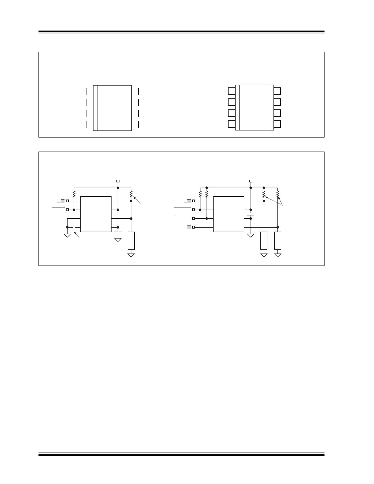
Package Types
Typical Application Schematics
MIC2505/-1/-2
8-Pin SOIC (M)
(Top View)
MIC2506
8-Pin SOIC (M)
(Top View)
1
2
3
4
8
7
6
5
OUT
IN
OUT
IN
CTL
FLG
GND
GATE
MIC2505/-1/-2
1
2
3
4
8
7
6
5
OUT A
IN
GND
OUT B
CTL A
FLG A
FLG B
CTL B
MIC2506
Single and Dual Switch/Circuit Breakers with Open-Load Detection and Fault Output
ON
OFF
MIC2505YM
Load
CTL
OUT
FLG
GND
OUT
GATE
IN
Optional
Output Delay
Capacitor
100
Nȍ
IN
FAULT
3.0V to 7.5V
Pull-up
Resistor
Nȍ
8
1
7
2
6
3
5
4
Optional
Open Load
Detect Resistor
(MIC2505YN or
MIC2505YM
onl
\
0.1μF
Load A
A ON
A OFF
MIC2506YM
CTL A OUT A
FLG A
FLG B
GND
CTL B OUT B
IN
FAULT A
3.0V to 7.5V
Pull-up
Resistors
NȍHDFK
8
1
7
2
6
3
5
4
Optional
Open Load
Dete
FWResistors
0.1μF
Load B
Nȍ
B ON
B OFF
FAULT B
Nȍ
2016 Microchip Technology Inc.
DS20005579A-page 3
MIC2505/6
Functional Block Diagrams
MIC2505 Series Block Diagram
MIC2506 Block Diagram
1.2V
REFERENCE
THERMAL
SHUTDOWN
OSC.
CHARGE
PUMP
OUT
UVLO
GATE
CONTROL
IN
OPEN LOAD
DETECT
FLG
CTL
CURRENT
LIMIT
GATE
GND
Not Included in
MIC2505-1, -2
MIC2505/2505-1/2505-2
1.2V
REFERENCE
THERMAL
SHUTDOWN
CHARGE
PUMP
OUT B
UVLO
GATE
CONTROL
IN
OPEN LOAD
DETECT
CTL A
GATE
CONTROL
OUT A
OPEN LOAD
DETECT
FLG B
CHARGE
PUMP
CTL B
OSC.
FLG A
CURRENT
LIMIT
CURRENT
LIMIT
GND
MIC2506

MIC2505/6
DS20005579A-page 4
2016 Microchip Technology Inc.
1.0
ELECTRICAL CHARACTERISTICS
Absolute Maximum Ratings †
Supply Voltage (V
IN
).................................................................................................................................................+8.0V
Fault Flag Voltage (V
FLG
) .........................................................................................................................................+7.5V
Fault Flag Current (I
FLG
) .........................................................................................................................................50 mA
Output Voltage (V
OUT
)................................................................................................................................................7.5V
Output Current (I
OUT
) .............................................................................................................................Internally Limited
Gate Voltage (V
GATE
) ........................................................................................................................................ V
IN
+ 15V
Control Input (V
CTL
) ................................................................................................................................... –0.3V to +15V
Operating Ratings ‡
Supply Voltage (V
IN
).................................................................................................................................. +3.0V to +7.5V
†
Notice: Stresses above those listed under “Absolute Maximum Ratings” may cause permanent damage to the device.
This is a stress rating only and functional operation of the device at those or any other conditions above those indicated
in the operational sections of this specification is not intended. Exposure to maximum rating conditions for extended
periods may affect device reliability.
‡ Notice:
The device is not guaranteed to function outside its operating ratings.
2016 Microchip Technology Inc.
DS20005579A-page 5
MIC2505/6
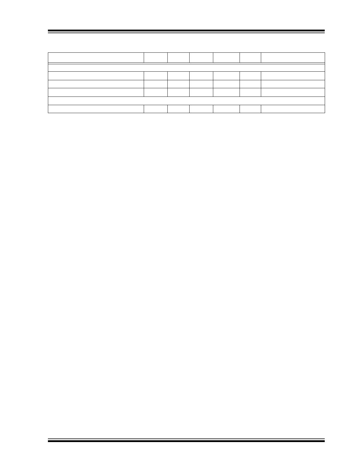
TABLE 1-1:
ELECTRICAL CHARACTERISTICS
Electrical Characteristics:
V
IN
= +5V, GATE = open, T
A
= 25°C, bold values are valid for –40°C ≤ T
A
≤ +85°C,
unless noted. (
Note 1
)
.
Parameters
Sym.
Min.
Typ.
Max.
Units
Conditions
Supply Current
I
DD
—
0.75
5
µA
MIC2505-1, MIC2506, V
CTL
=
logic 0, OUT = open.
—
110
160
µA
MIC2505-1, MIC2506, V
CTL
=
logic 1, OUT = open.
—
110
160
µA
MIC2505-2, V
CTL
= logic 0,
OUT = open.
—
0.75
5
µA
MIC2505-2, V
CTL
= logic 1,
OUT = open.
Control Input Voltage
V
CTL
—
2.1
2.4
V
V
CTL
= logic 0 to logic 1
transition
0.8
1.9
—
V
V
CTL
= logic 1 to logic 0
transition
Control Input Current
I
CTL
—
0.01
1
µA
V
CTL
= logic 0
—
0.01
1
µA
V
CTL
= logic 1
Control Input Capacitance
C
CTL
—
1
—
pF
—
Output MOSFET Resistance
R
DS(ON)
—
30
50
mΩ
MIC2505 Series, V
IN
= 5V,
T
A
= 25°C.
—
—
60
mΩ
MIC2505 Series, V
IN
= 5V,
–40°C < T
A
< +85°C.
—
35
60
mΩ
MIC2505 Series, V
IN
= 3.3V,
T
A
= 25°C.
—
—
75
mΩ
MIC2505 Series, V
IN
= 3.3V,
–40°C < T
A
< +85°C.
—
75
125
mΩ
MIC2506, V
IN
= 5V,
T
A
= 25°C.
—
—
150
mΩ
MIC2506, V
IN
= 5V,
–40°C < T
A
< +85°C.
—
80
135
mΩ
MIC2506, V
IN
= 3.3V,
T
A
= 25°C.
—
—
165
mΩ
MIC2506, V
IN
= 3.3V,
–40°C < T
A
< +85°C.
Output Turn-On Delay
t
ON
200
850
2000
µs
MIC2505 Series, R
L
= 10Ω,
C
GATE
= 0.
100
700
2000
µs
MIC2506, R
L
= 10Ω each
output.
Output Turn-On Rise Time
t
R
500
3000
7500
µs
MIC2505 Series, R
L
= 10Ω,
C
GATE
= 0.
200
2000
6000
µs
MIC2506, R
L
= 10Ω each
output.
Note 1:
Devices are ESD protected; however, handling precautions recommended. All limits guaranteed by testing
or statistical analysis.
2:
MIC2505-1 and -2 versions have no open load detect feature.
3:
Open load threshold is the output voltage (V
OUT
) where FLG becomes active (low) when CTL is low. OUT
is pulled high by a 100 kΩ external resistor to V
IN
.
MIC2505/6
DS20005579A-page 6
2016 Microchip Technology Inc.
Output Turn-Off Delay
t
OFF
—
0.7
20
µs
MIC2505 Series, R
L
= 10Ω,
C
GATE
= 0.
—
0.8
20
µs
MIC2506, R
L
= 10Ω each
output.
Output Turn-Off Fall Time
t
F
—
1.5
20
µs
MIC2505 Series, R
L
= 10Ω,
C
GATE
= 0.
—
0.7
20
µs
MIC2506, R
L
= 10Ω each
output.
Output Leakage Current
I
LKG
—
—
10
µA
—
Current Limit Threshold
I
LIM
2
4
—
A
MIC2505 Series
1
2
3
A
MIC2506
Open Load Threshold (
Note 2
)
V
OPENL_TH
0.5
1
1.5
V
V
CTL
= logic low,
Note 3
Overtemperature Shutdown
Threshold
T
SD
—
135
—
°C
T
J
increasing
—
125
—
°C
T
J
decreasing
Error Flag Output Resistance
R
FLG
—
10
25
Ω
V
IN
= 5V, I
L
= 10 mA
—
15
40
Ω
V
IN
= 3.3V, I
L
= 10 mA
Error Flag Off Current
I
FLG_OFF
—
0.01
1
µA
V
FLAG
= 5V
UVLO Threshold
V
UVLO_TH
2.2
2.5
3.0
V
V
IN
increasing
UVLO Hysteresis
V
UVLO_TH_
HYST
—
215
—
mV
MIC2505
—
235
—
mV
MIC2506
TABLE 1-1:
ELECTRICAL CHARACTERISTICS (CONTINUED)
Electrical Characteristics:
V
IN
= +5V, GATE = open, T
A
= 25°C, bold values are valid for –40°C ≤ T
A
≤ +85°C,
unless noted. (
Note 1
)
.
Parameters
Sym.
Min.
Typ.
Max.
Units
Conditions
Note 1:
Devices are ESD protected; however, handling precautions recommended. All limits guaranteed by testing
or statistical analysis.
2:
MIC2505-1 and -2 versions have no open load detect feature.
3:
Open load threshold is the output voltage (V
OUT
) where FLG becomes active (low) when CTL is low. OUT
is pulled high by a 100 kΩ external resistor to V
IN
.
2016 Microchip Technology Inc.
DS20005579A-page 7
MIC2505/6
TEMPERATURE SPECIFICATIONS
Parameters
Sym.
Min.
Typ.
Max.
Units
Conditions
Temperature Ranges
Ambient Operating Temperature
T
A
–40
—
+85
°C
—
Storage Temperature Range
T
S
–65
—
+150
°C
—
Lead Temperature
—
—
—
+260
°C
Soldering, 5s
Package Thermal Resistances
Thermal Resistance, SOIC
JA
—
160
—
°C/W
—
MIC2505/6
DS20005579A-page 8
2016 Microchip Technology Inc.
2.0
TYPICAL PERFORMANCE CURVES
FIGURE 2-1:
MIC2505 Turn-On, Turn-Off
Characteristics.
FIGURE 2-2:
Output On Resistance vs.
Supply Voltage.
FIGURE 2-3:
Output On Resistance vs.
Temperature.
FIGURE 2-4:
MIC2506 Turn-On, Turn-Off
Characteristics.
FIGURE 2-5:
UVLO Threshold Voltage vs.
Temperature.
FIGURE 2-6:
Error Flag Voltage vs. Error
Flag Current.
Note:
The graphs and tables provided following this note are a statistical summary based on a limited number of
samples and are provided for informational purposes only. The performance characteristics listed herein
are not tested or guaranteed. In some graphs or tables, the data presented may be outside the specified
operating range (e.g., outside specified power supply range) and therefore outside the warranted range.
-2
0
2
4
TIME (
μs)
-5
0
5
10
CONTROL (V)
-2
0
2
4
6
-2
0
2
4
6
OUTPUT (V)
TIME (ms)
R
L
= 5
Ω
(I
L
= 1A)
0
20
40
60
80
100
2
3
4
5
6
7
8
OUTPUT RESISTANCE (m
Ω
)
SUPPLY VOLTAGE (V)
MIC2505
MIC2506
0
20
40
60
80
100
-40 -20
0
20
40
60
80 100
ON RESISTANCE (m
Ω
)
TEMPERATURE (
°C)
MIC2506
MIC2505
-1
0
1
2
TIME (
μs)
-5
0
5
10
CONTROL (V)
-2
0
2
4
6
-2
0
2
4
6
OUTPUT (V)
TIME (ms)
R
L
= 5
Ω
(I
L
= 1A)
1.5
2.0
2.5
3.0
-40 -20
0
20
40
60
80 100
THRESHOLD VOLTAGE (V)
TEMPERATURE (
°C)
V
IN
RISING
V
IN
FALLING
0
100
200
300
400
0.1
1
10
100
ERROR FLAG VOLTAGE (mV)
ERROR FLAG CURRENT (mA)
FLG = ACTIVE
V
DD
= 3.3V
V
DD
= 5V
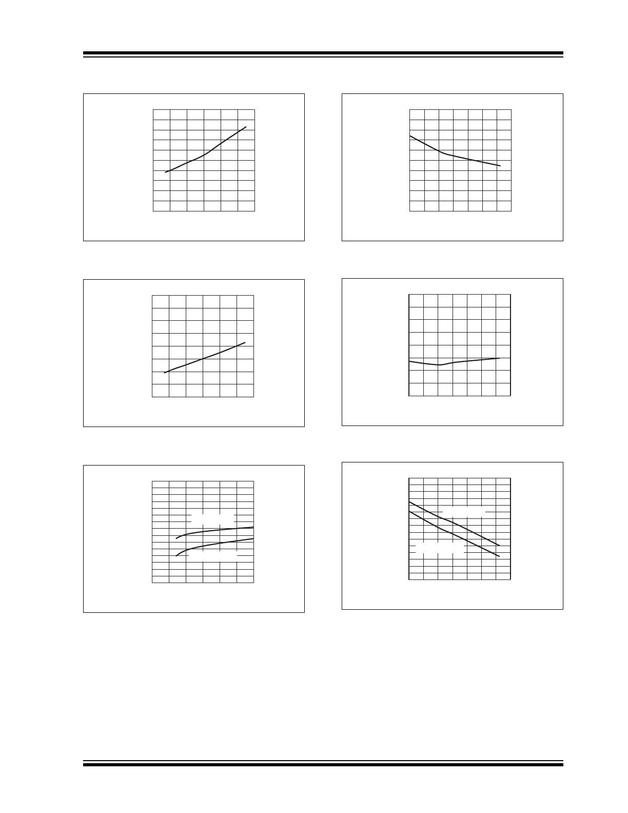
2016 Microchip Technology Inc.
DS20005579A-page 9
MIC2505/6
FIGURE 2-7:
On-State Supply Current vs.
Supply Voltage.
FIGURE 2-8:
Off-State Supply Current vs.
Supply Voltage.
FIGURE 2-9:
Control Threshold vs.
Supply Voltage.
FIGURE 2-10:
On-State Supply Current vs.
Temperature.
FIGURE 2-11:
Off-State Supply Current vs.
Temperature.
FIGURE 2-12:
Control Threshold vs.
Temperature.
0
20
40
60
80
100
120
140
160
180
200
2
3
4
5
6
7
8
SUPPLY CURRENT (
μ
A)
SUPPLY VOLTAGE (V)
0
0.5
1.0
1.5
2.0
2
3
4
5
6
7
8
SUPPLY CURRENT (
μ
A)
SUPPLY VOLTAGE (V)
1.0
1.5
2.0
2.5
2
3
4
5
THRESHOLD VOLTAGE (V)
SUPPLY VOLTAGE (V)
V
CTL
RISING
V
CTL
FALLING
0
20
40
60
80
100
120
140
160
180
200
-40 -20
0
20
40
60
80 100
SUPPLY CURRENT (
μ
A)
TEMPERATURE (
°C)
0
0.5
1.0
1.5
2.0
-40 -20
0
20
40
60
80 100
SUPPLY CURRENT (
μ
A)
TEMPERATURE (
°C)
1
1.5
2.0
2.5
-40 -20
0
20
40
60
80 100
THRESHOLD VOLTAGE (V)
TEMPERATURE (
°C)
V
CTL
RISING
V
CTL
FALLING
MIC2505/6
DS20005579A-page 10
2016 Microchip Technology Inc.
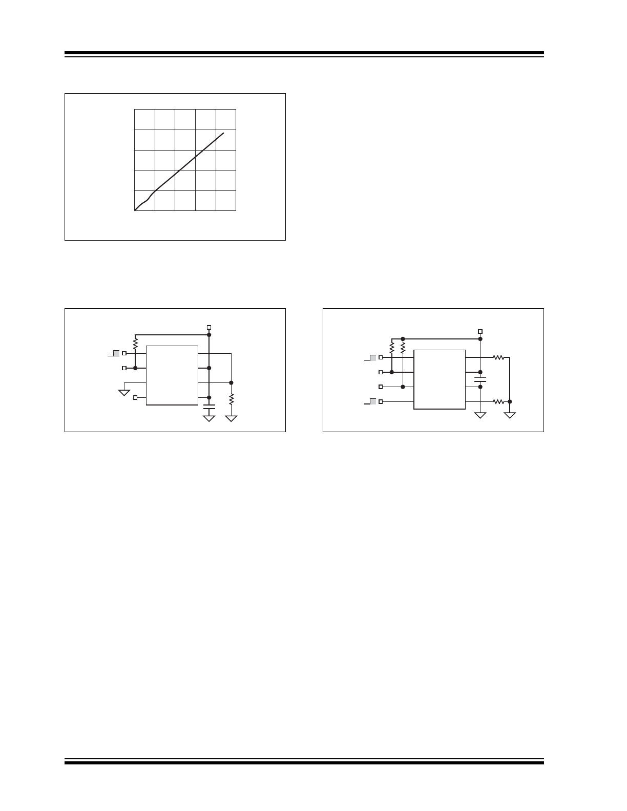
FIGURE 2-13:
MIC2505 Turn-On Delay
with External Gate Capacitance
.
3.0
TEST CIRCUITS
FIGURE 3-1:
MIC2505 Series Test Circuit.
FIGURE 3-2:
MIC2506 Test Circuit.
0
200
400
600
800
1000
0
50
100
150
200
250
TURN-ON DELAY (ms)
CAPACITANCE (nF)
MIC2505/-1/-2
CTL
OUT
FLG
GND
OUT
GATE
IN
IN
+5V
1μF
10
Ω
V
FLG
10k
Ω
MIC2506YM
CTL A OUT A
FLG A
GND
CTL B OUT B
IN
FLG B
B ON
B OFF
A ON
A OFF
+5V
1μF
10
Ω
10
Ω
10k
Ω
V
FLG A
V
FLG B
10k
Ω