
© 2007 Microchip Technology Inc.
DS22036B-page 1
MCP73811/2
Features
• Complete Linear Charge Management Controller
- Integrated Pass Transistor
- Integrated Current Sense
- Integrated Reverse Discharge Protection
• Constant Current / Constant Voltage Operation
with Thermal Regulation
• High Accuracy Preset Voltage Regulation: + 1%
• Voltage Regulation: 4.20V
• Selectable Charge Current:
- MCP73811: 85 mA / 450 mA
• Programmable Charge Current:
- MCP73812: 50 mA - 500 mA
• Minimum External Components Required:
- MCP73811: 2 Ceramic Capacitors
- MCP73812: 2 Ceramic Capacitors and
1 Resistor
• No Preconditioning
• External End-of-Charge Control
• Automatic Power-Down when Input Power
Removed
• Active High Charge Enable
• Temperature Range:
- -40°C to +85°C
• Packaging:
- 5-Lead SOT-23
Applications
• Low-Cost Lithium-Ion/Lithium-Polymer Battery
Chargers
• Rechargeable Toys
• Electronic Cigarettes
• Bluetooth Headsets
• USB Chargers
Description
The MCP73811/2 devices are linear charge manage-
ment controllers that are designed for use in space
limited and cost sensitive applications. The
MCP73811/2 provide specific charge algorithms for
single cell Li-Ion or Li-Polymer battery to achieve
optimal capacity in the shortest charging time possible.
Along with its small physical size, the low number of
external components required make the MCP73811/2
ideally suited for portable applications. For applications
charging from a USB port, the MCP73811 adheres to
all the specifications governing the USB power bus.
The MCP73811/2 employ a constant current/constant
voltage charge algorithm. The constant voltage regula-
tion is fixed at 4.20V, with a tight regulation tolerance of
1%. For the MCP73811, the constant current value is
selected as 85 mA (low power USB port) or 450 mA
(high power USB port) with a digital input signal on the
PROG input. For the MCP73812, the constant current
value is set with one external resistor. The
MCP73811/2 limit the charge current based on die
temperature during high power or high ambient
conditions. This thermal regulation optimizes the
charge cycle time while maintaining device reliability.
The MCP73811/2 are fully specified over the ambient
temperature range of -40°C to +85°C. The
MCP73811/2 are available in a 5-Lead, SOT-23
package.
Package Types
V
DD
V
BAT
5
5-Pin SOT-23
1
3
4
2
CE
PROG
V
SS
Simple, Miniature Single-Cell, Fully Integrated
Li-Ion / Li-Polymer Charge Management Controllers
MCP73811/2
DS22036B-page 2
© 2007 Microchip Technology Inc.
Typical Applications
Functional Block Diagram
CE
V
DD
V
SS
PROG
V
BAT
+
-
Single
Li-Ion
Cell
4
MCP73812
5
3
1
500 mA Li-Ion Battery Charger
2
2 k
Ω
CE
V
DD
V
SS
PROG
V
BAT
+
-
Single
Li-Ion
Cell
4
MCP73811
5
3
1
1 µF
450 mA Li-Ion Battery Charger
2
V
IN
1 µF
1 µF
V
IN
1 µF
+
-
Reference
Generator
V
REF
(1.21V)
V
BAT
V
DD
V
BAT
G=0.001
V
SS
Direction
Control
+
-
Direction
Control
6µA
+
-
CA
157.3 k
Ω
388.7 k
Ω
+
-
VA
CE
Charge
Enable
2.7 k
Ω
PROG
111 k
Ω
528.6 k
Ω
MCP73811
MCP73812
12 k
Ω
© 2007 Microchip Technology Inc.
DS22036B-page 3
MCP73811/2
1.0
ELECTRICAL
CHARACTERISTICS
Absolute Maximum Ratings†
V
DD
N
................................................................................7.0V
All Inputs and Outputs w.r.t. V
SS
............... -0.3 to (V
DD
+0.3)V
Maximum Junction Temperature, T
J
............ Internally Limited
Storage temperature .....................................-65°C to +150°C
ESD protection on all pins
Human Body Model (1.5 kW in Series with 100 pF)
......≥ 4 kV
Machine Model (200pF, No Series Resistance) ..............400V
† Notice: Stresses above those listed under “Maximum
Ratings” may cause permanent damage to the device.
This is a stress rating only and functional operation of
the device at those or any other conditions above those
indicated in the operational listings of this specification
is not implied. Exposure to maximum rating conditions
for extended periods may affect device reliability.
DC CHARACTERISTICS
Electrical Specifications: Unless otherwise indicated, all limits apply for V
DD
= [V
REG
(typ.) + 0.3V] to 6V,
T
A
= -40°C to +85°C. Typical values are at +25°C, V
DD
= [V
REG
(typ.) + 1.0V]
Parameters
Sym
Min
Typ
Max
Units
Conditions
Supply Input
Supply Voltage
V
DD
3.75
—
6
V
Supply Current
I
SS
—
1000
1500
µA
Charging
—
50
100
µA
Standby (CE = V
SS
)
—
1.2
5
µA
Shutdown
(V
DD
< V
BAT
- 100 mV)
Voltage Regulation (Constant Voltage Mode)
Regulated Output Voltage
V
REG
—
4.20
—
V
V
DD
=[V
REG
(Typ)+1V]
I
OUT
=10 mA
Output Voltage Tolerance
V
RTOL
-1
—
+1
%
T
A
=-5°C to +55°C
Line Regulation
|(ΔV
BAT
/V
BAT
)
/
ΔV
DD
|
—
0.09
0.30
%/V
V
DD
=[V
REG
(Typ)+1V] to 6V
I
OUT
=10 mA
Load Regulation
|ΔV
BAT
/V
BAT
|
—
0.09
0.30
%
I
OUT
=10 mA to 50 mA
V
DD
=[V
REG
(Typ)+1V]
Supply Ripple Attenuation
PSRR
—
52
—
dB
I
OUT
=10 mA, 10 Hz to 1 kHz
—
47
—
dB
I
OUT
=10 mA, 10 Hz to 10 kHz
—
22
—
dB
I
OUT
=10 mA, 10 Hz to 1 MHz
Current Regulation (Fast Charge Constant-Current Mode)
Fast Charge Current
I
REG
—
85
—
mA
MCP73811 - PROG = Low
Regulation
—
450
—
mA
MCP73811 - PROG = High
—
50
—
mA
MCP73812 - PROG = 20 k
Ω
—
100
—
mA
MCP73812 - PROG = 10 k
Ω
—
500
—
mA
MCP73812 - PROG = 2 k
Ω
Charge Current Tolerance
I
RTOL
-10
—
+10
%
T
A
=-5°C to +55°C
Pass Transistor ON-Resistance
ON-Resistance
R
DSON
—
400
—
m
Ω
V
DD
= 3.75V, T
J
= 105°C
Battery Discharge Current
Output Reverse Leakage
I
DISCHARGE
Current
—
0.5
2
µA
Shutdown
(V
DD
< V
BAT
- 100 mV)
MCP73811/2
DS22036B-page 4
© 2007 Microchip Technology Inc.
TEMPERATURE SPECIFICATIONS
Charge Enable (CE), PROG Input - MCP73811
Input High Voltage Level
V
IH
2
—
—
V
Input Low Voltage Level
V
IL
—
—
0.8
V
Input Leakage Current
I
LK
—
0.01
1
µA
V
CE
= V
DD
, V
PROG
= V
DD
PROG Input - MCP73812
Charge Impedance Range
R
PROG
2
—
20
k
Ω
MCP73812
Automatic Power Down (Direction Control)
Automatic Power Down
Entry Threshold
V
PD
V
BAT
+
10 mV
V
BAT
+
50 mV
—
V
2.3V < V
BAT
< V
REG
V
DD
Falling
Automatic Power Down
Exit Threshold
V
PDEXIT
—
V
BAT
+
150 mV
V
BAT
+
250 mV
V
2.3V < V
BAT
< V
REG
V
DD
Rising
Thermal Shutdown
Die Temperature
T
SD
—
150
—
°C
Die Temperature
T
SDHYS
—
10
—
°C
Hysteresis
Electrical Specifications: Unless otherwise indicated, all limits apply for V
DD
= [V
REG
(typ.) + 0.3V] to 6V.
Typical values are at +25°C, V
DD
= [V
REG
(typ.) + 1.0V]
Parameters
Sym
Min
Typ
Max
Units
Conditions
Temperature Ranges
Specified Temperature Range
T
A
-40
—
+85
°C
Operating Temperature Range
T
J
-40
—
+125
°C
Storage Temperature Range
T
A
-65
—
+150
°C
Thermal Package Resistances
Thermal Resistance, 5-Lead, SOT-23
θ
JA
—
230
—
°C/W
4-Layer JC51-7 Standard Board,
Natural Convection
DC CHARACTERISTICS (Continued)
Electrical Specifications: Unless otherwise indicated, all limits apply for V
DD
= [V
REG
(typ.) + 0.3V] to 6V,
T
A
= -40°C to +85°C. Typical values are at +25°C, V
DD
= [V
REG
(typ.) + 1.0V]
Parameters
Sym
Min
Typ
Max
Units
Conditions
© 2007 Microchip Technology Inc.
DS22036B-page 5
MCP73811/2
2.0
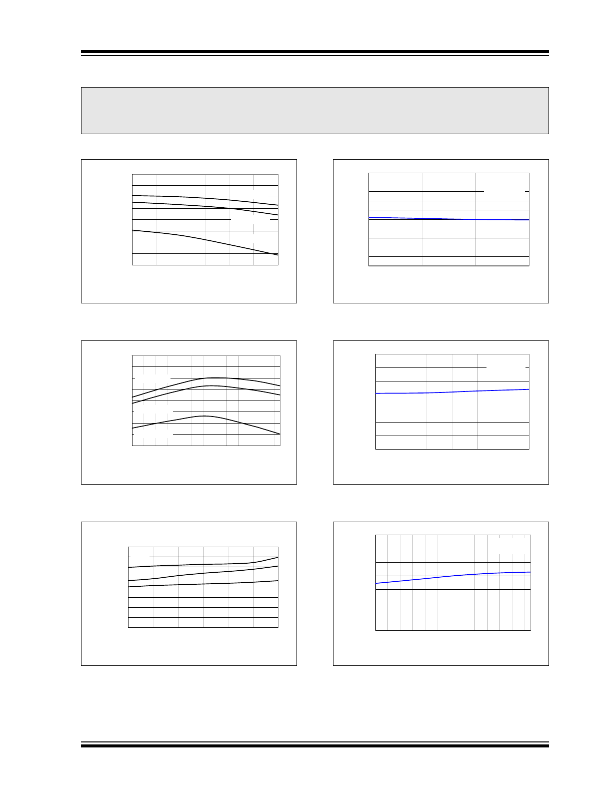
TYPICAL PERFORMANCE CURVES
Note: Unless otherwise indicated, V
DD
= [V
REG
(typ.) + 1V], I
OUT
= 10 mA and T
A
= +25°C, Constant-voltage mode.
FIGURE 2-1:
Battery Regulation Voltage
(V
BAT
) vs. Supply Voltage (V
DD
).
FIGURE 2-2:
Battery Regulation Voltage
(V
BAT
) vs. Ambient Temperature (T
A
).
FIGURE 2-3:
Output Leakage Current
(I
DISCHARGE
) vs. Battery Regulation Voltage
(V
BAT
).
FIGURE 2-4:
Charge Current (I
OUT
) vs.
Supply Voltage (V
DD
) - MCP73811.
FIGURE 2-5:
Charge Current (I
OUT
) vs.
Supply Voltage (V
DD
) - MCP73811.
FIGURE 2-6:
Charge Current (I
OUT
) vs.
Ambient Temperature (T
A
) - MCP73811.
Note:
The graphs and tables provided following this note are a statistical summary based on a limited number of
samples and are provided for informational purposes only. The performance characteristics listed herein
are not tested or guaranteed. In some graphs or tables, the data presented may be outside the specified
operating range (e.g., outside specified power supply range) and therefore outside the warranted range.
4.170
4.175
4.180
4.185
4.190
4.195
4.200
4.205
4.210
4.50
4.75
5.00
5.25
5.50
5.75
6.00
Supply Voltage (V)
B
attery
R
e
g
u
la
ti
on
V
o
lta
g
e
(V
)
I
OUT
= 10 mA
I
OUT
= 100 mA
I
OUT
= 450 mA
4.170
4.175
4.180
4.185
4.190
4.195
4.200
4.205
4.210
-40
-30
-20
-10
0
10
20
30
40
50
60
70
80
Ambient Temperature (°C)
Battery R
egu
la
ti
on
V
o
lt
a
g
e
(V
)
I
OUT
= 10 mA
I
OUT
= 100 mA
I
OUT
= 450 mA
0.00
0.05
0.10
0.15
0.20
0.25
0.30
0.35
0.40
3.00
3.20
3.40
3.60
3.80
4.00
4.20
Battery Regulation Voltage (V)
O
u
tpu
t Le
akag
e C
u
rre
nt (µA
)
+85°C
-40°C
+25°C
80
81
82
83
84
85
86
87
88
89
90
4.5
4.75
5
5.25
5.5
5.75
6
Supply Voltage (V)
C
h
arg
e Cur
rent
(mA)
PROG = Low
Temp = +25°C
425
430
435
440
445
450
455
460
4.5
4.75
5
5.25
5.5
5.75
6
Supply Voltage (V)
Ch
ar
g
e Cu
rr
e
nt
(m
A)
PROG = High
Temp = 25°C
65
70
75
80
85
90
95
100
-40 -30 -20 -10 0 10 20 30 40 50 60 70 80
Ambient Temperature (°C)
Ch
ar
g
e Cu
rr
en
t (
m
A)
PROG = Low
V
DD
= 5V
MCP73811/2
DS22036B-page 6
© 2007 Microchip Technology Inc.
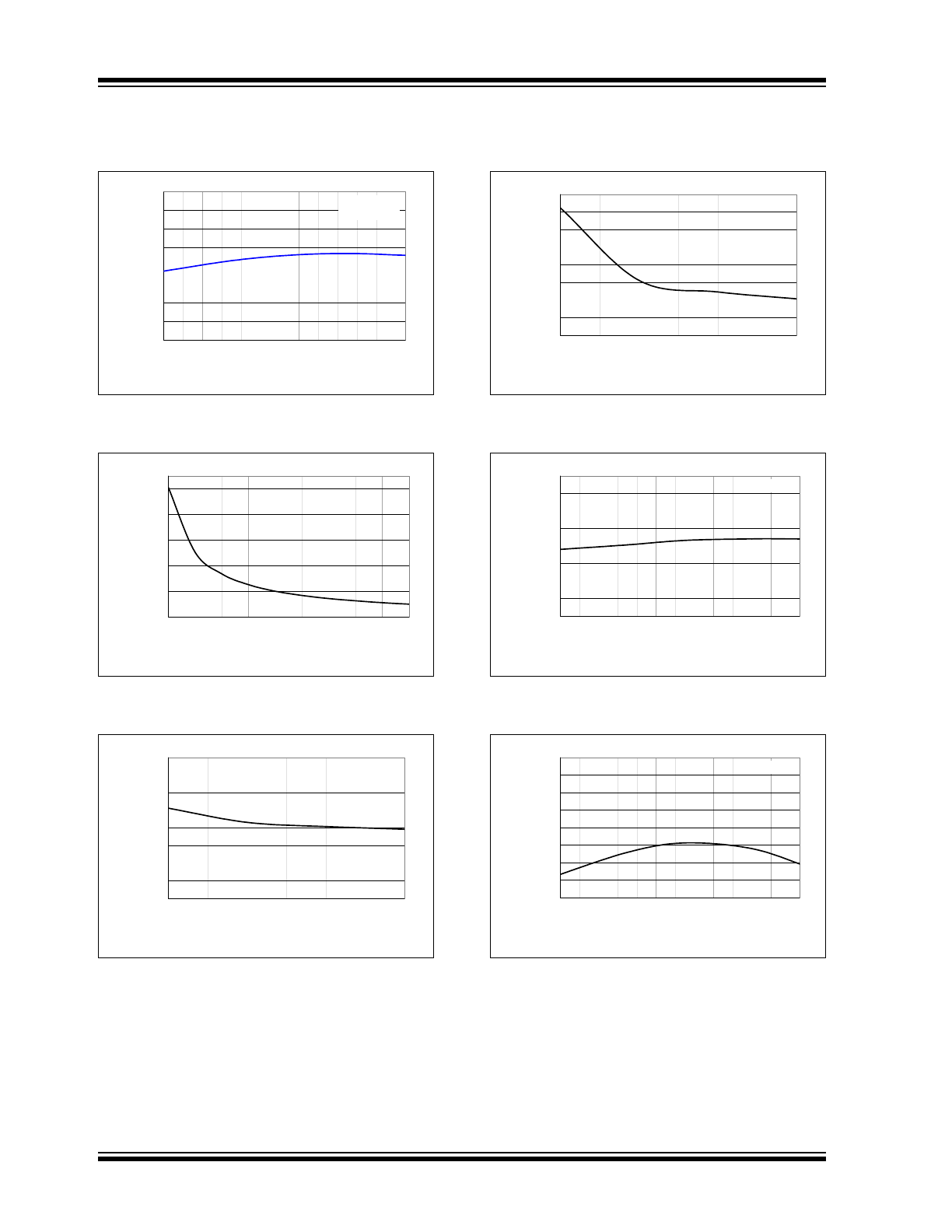
Typical Performance Curves (Continued)
Note: Unless otherwise indicated, V
DD
= [V
REG
(typ.) + 1V], I
OUT
= 10 mA and T
A
= +25°C, Constant-voltage mode.
FIGURE 2-7:
Charge Current (I
OUT
) vs.
Ambient Temperature (T
A
) - MCP73811.
FIGURE 2-8:
Charge Current (I
OUT
) vs.
Programming Resistor (R
PROG
) - MCP73812.
FIGURE 2-9:
Charge Current (I
OUT
) vs.
Supply Voltage (V
DD
) - MCP73812.
FIGURE 2-10:
Charge Current (I
OUT
) vs.
Supply Voltage (V
DD
) - MCP73812.
FIGURE 2-11:
Charge Current (I
OUT
) vs.
Ambient Temperature (T
A
) - MCP73812.
FIGURE 2-12:
Charge Current (I
OUT
) vs.
Ambient Temperature (T
A
) - MCP73812.
400
410
420
430
440
450
460
470
480
-40 -30 -20 -10 0 10 20 30 40 50 60 70 80
Ambient Temperature (°C)
Ch
arge
Curre
nt (mA)
PROG = High
V
DD
= 5V
0
50
100
150
200
250
300
350
400
450
500
550
2
4
6
8
10
12
14
16
18
20
Programming Resistor (kΩ)
C
h
a
rge
Cu
rren
t (m
A
)
96
97
98
99
100
101
102
103
104
4.50
4.75
5.00
5.25
5.50
5.75
6.00
Supply Voltage (V)
Ch
arg
e C
u
rre
nt (mA)
R
PROG
= 10 kΩ
500
502
504
506
508
510
512
514
516
4.50
4.75
5.00
5.25
5.50
5.75
6.00
Supply Voltage (V)
Ch
ar
g
e
C
u
rr
ent
(
m
A)
R
PROG
= 2 kΩ
96
97
98
99
100
101
102
103
104
-40
-30
-20
-10
0
10
20
30
40
50
60
70
80
Ambient Temperature (°C)
Ch
arg
e Cu
rren
t (mA)
R
PROG
= 10 kΩ
500
502
504
506
508
510
512
514
516
-40
-30
-20
-10
0
10
20
30
40
50
60
70
80
Ambient Temperature (°C)
C
h
arg
e Cur
rent
(mA)
R
PROG
= 2 kΩ
© 2007 Microchip Technology Inc.
DS22036B-page 7
MCP73811/2
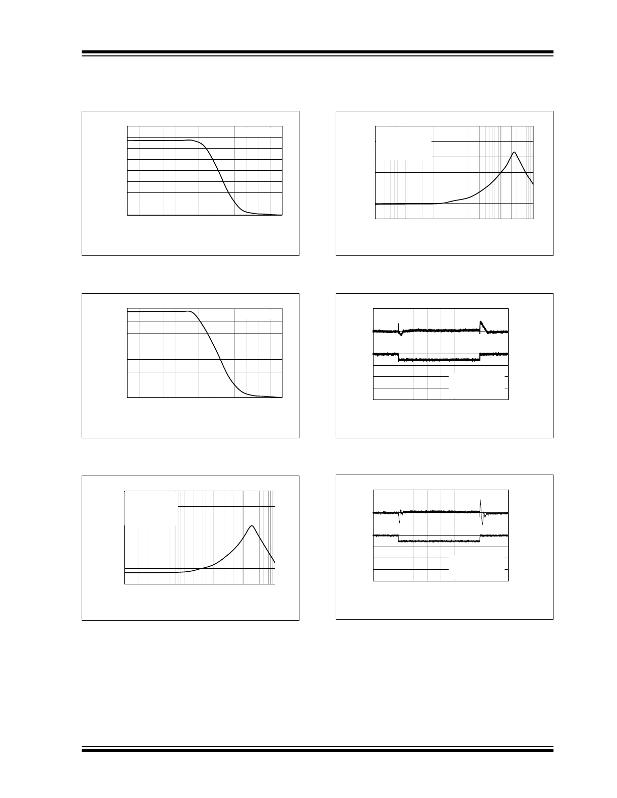
Typical Performance Curves (Continued)
Note: Unless otherwise indicated, V
DD
= [V
REG
(typ.) + 1V], I
OUT
= 10 mA and T
A
= +25°C, Constant-voltage mode.
FIGURE 2-13:
Charge Current (I
OUT
) vs.
Junction Temperature (T
J
) - MCP73812.
FIGURE 2-14:
Charge Current (I
OUT
) vs.
Junction Temperature (T
J
) - MCP73812.
FIGURE 2-15:
Power Supply Ripple
Rejection (PSRR).
FIGURE 2-16:
Power Supply Ripple
Rejection (PSRR).
FIGURE 2-17:
Line Transient Response.
FIGURE 2-18:
Line Transient Response.
0
15
30
45
60
75
90
105
120
25
35
45
55
65
75
85
95
10
5
11
5
12
5
13
5
14
5
15
5
Junction Temperature (°C)
C
h
a
rge Cu
rren
t (
m
A
)
R
PROG
= 10 kΩ
0
75
150
225
300
375
450
525
25
35
45
55
65
75
85
95
10
5
11
5
12
5
13
5
14
5
15
5
Junction Temperature (°C)
Ch
ar
g
e C
u
rr
ent
(
m
A)
R
PROG
= 2 kΩ
-60
-50
-40
-30
-20
-10
0
0.01
0.1
1
10
100
1000
Frequency (kHz)
Attenuation (dB)
V
AC
= 100 mVp-p
I
OUT
= 10 mA
C
OUT
= 4.7 μF, X7R
Ceramic
-60
-50
-40
-30
-20
-10
0
0.01
0.1
1
10
100
1000
Frequency (kHz)
Att
en
u
ation (d
B
)
V
AC
= 100 mVp-p
I
OUT
= 100 mA
C
OUT
= 4.7 µF, X7R
Ceramic
-2
0
2
4
6
8
10
12
14
0
20
40
60
80
10
0
12
0
14
0
16
0
18
0
20
0
Time (µs)
S
o
u
rce Voltage
(V
)
-0.30
-0.25
-0.20
-0.15
-0.10
-0.05
0.00
0.05
0.10
Ou
tput R
ipple (V)
I
OUT
= 10 mA
C
OUT
= 4.7 µF, X7R
Ceramic
-2
0
2
4
6
8
10
12
14
0
20
40
60
80
10
0
12
0
14
0
16
0
18
0
20
0
Time (µs)
Sour
ce Vol
tag
e
(V
)
-0.30
-0.25
-0.20
-0.15
-0.10
-0.05
0.00
0.05
0.10
O
u
tput Ripple
(V
)
I
OUT
= 100 mA
C
OUT
= 4.7 µF, X7R
Ceramic
MCP73811/2
DS22036B-page 8
© 2007 Microchip Technology Inc.
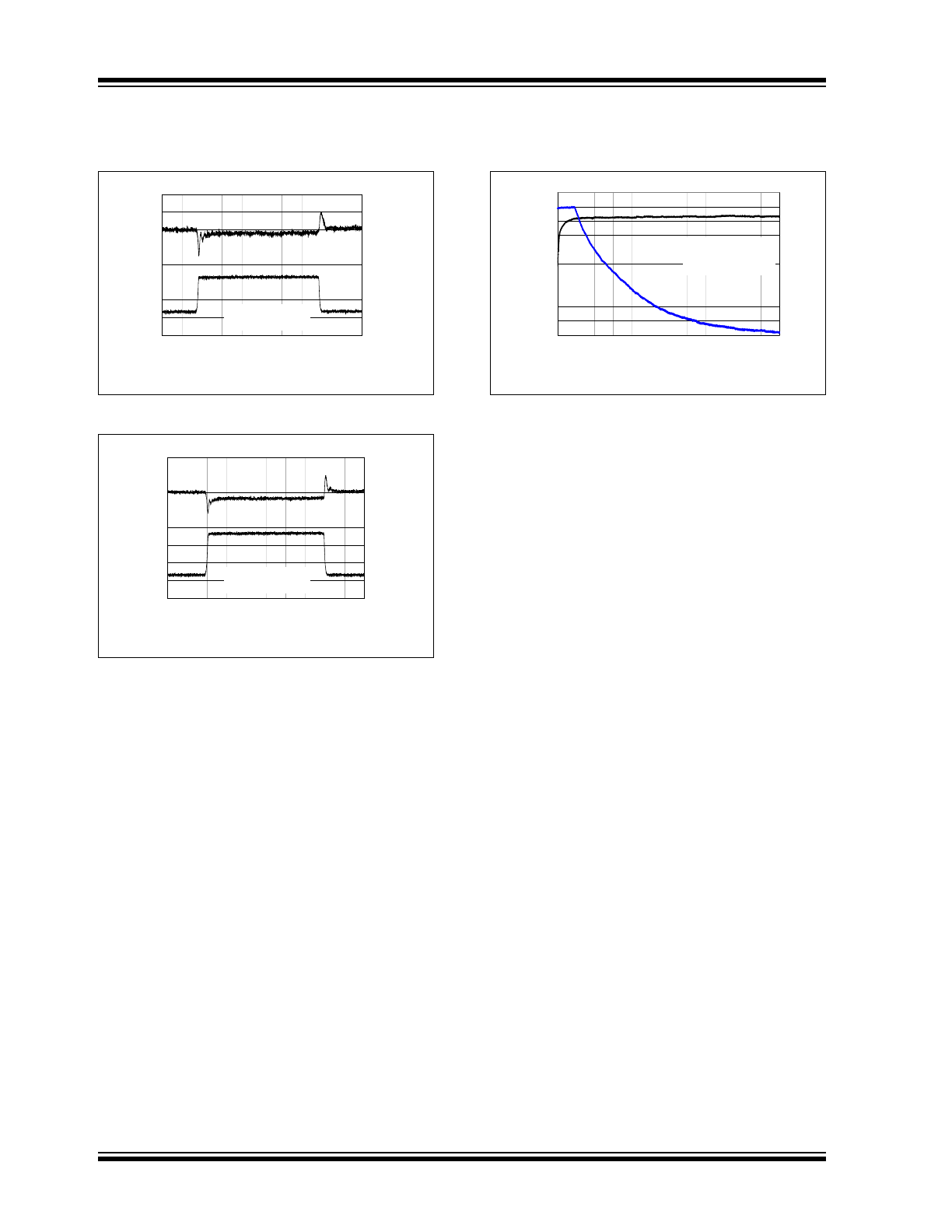
Typical Performance Curves (Continued)
Note: Unless otherwise indicated, V
DD
= [V
REG
(typ.) + 1V], I
OUT
= 10 mA and T
A
= +25°C, Constant-voltage mode.
FIGURE 2-19:
Load Transient Response.
FIGURE 2-20:
Load Transient Response.
FIGURE 2-21:
Typical Charge Profile
(950 mAh) Li-Ion Battery.
-0.05
0.00
0.05
0.10
0.15
0.20
0.25
0.30
0.35
0
20
40
60
80
10
0
12
0
14
0
16
0
18
0
20
0
Time (µs)
O
u
tput Cur
rent (A
)
-0.12
-0.10
-0.08
-0.06
-0.04
-0.02
0.00
0.02
0.04
Ou
tput R
ipple (V)
C
OUT
= 4.7 µF, X7R
Ceramic
-0.20
0.00
0.20
0.40
0.60
0.80
1.00
1.20
1.40
0
20
40
60
80
10
0
12
0
14
0
16
0
18
0
20
0
Time (µs)
Output C
u
rr
ent
(A)
-0.30
-0.25
-0.20
-0.15
-0.10
-0.05
0.00
0.05
0.10
Ou
tput R
ipple (V)
C
OUT
= 4.7 µF, X7R
Ceramic
0.0
1.0
2.0
3.0
4.0
5.0
0
15
30
45
60
75
90
105
120
135
150
165
180
Time (Minutes)
Battery
V
o
lt
a
g
e (V
)
Charge Current
(mA)
0
100
200
300
400
500
MCP73812T-420I/OT
V
DD
= 5.0V
R
PROG
= 2 kΩ
© 2007 Microchip Technology Inc.
DS22036B-page 9
MCP73811/2
3.0
PIN DESCRIPTION
The descriptions of the pins are listed in Table 3-1.
TABLE 3-1:
PIN FUNCTION TABLES
3.1
Charge Enable Input (CE)
A logic High enables battery charging. A logic Low
disables battery charging. The charge enable input is
compatible with 1.8V logic.
3.2
Battery Management 0V Reference
(V
SS
)
Connect to negative terminal of battery and input
supply.
3.3
Battery Charge Control Output
(V
BAT
)
Connect to positive terminal of battery. Drain terminal
of internal P-channel MOSFET pass transistor. Bypass
to V
SS
with a minimum of 1 µF to ensure loop stability
when the battery is disconnected.
3.4
Battery Management Input Supply
(V
DD
)
A supply voltage of [V
REG
(typ.) + 0.3V] to 6V is
recommended. Bypass to V
SS
with a minimum of 1 µF.
3.5
Current Regulation Set (PROG)
For the MCP73811, the current regulation set input
(PROG) functions as a digital input selection. A logic
Low selects a 85 mA charge current; a logic High
selects a 450 mA charge current.
For the MCP73812, the charge current is set by placing
a resistor from PROG to V
SS
.
Pin Number
Symbol
Function
SOT-23-5
1
CE
Active High Charge Enable
2
V
SS
Battery Management 0V Reference
3
V
BAT
Battery Charge Control Output
4
V
DD
Battery Management Input Supply
5
PROG
Current Regulation Set and Charge Control Enable
MCP73811/2
DS22036B-page 10
© 2007 Microchip Technology Inc.
4.0
DEVICE OVERVIEW
The MCP73811/2 are simple, but fully integrated linear
charge management controllers.
Figure 4-1
depicts the
operational flow algorithm.
FIGURE 4-1:
Flow Chart.
4.1
Undervoltage Lockout (UVLO)
The MCP73811/2 does not have an internal under
voltage lockout (UVLO) circuit.
4.2
Charge Qualification
When the input power is applied, the input supply must
rise 150 mV above the battery voltage before the
MCP73811/2 becomes operational.
The automatic power down circuit places the device in
a shutdown mode if the input supply falls to within
+50 mV of the battery voltage.
The automatic circuit is always active. Whenever the
input supply is within +50 mV of the voltage at the V
BAT
pin, the MCP73811/2 is placed in a shutdown mode.
During power down condition, the battery reverse dis-
charge current is less than 2 µA.
For a charge cycle to begin, the automatic power down
conditions must be met and the charge enable input
must be above the input high threshold.
4.3
PRECONDITIONING
The MCP73811/2 does not support preconditioning of
deeply depleted cells.
4.4
Constant Current MODE - Fast
Charge
During the constant current mode, the selected
(MCP73811) or programmed (MCP73812) charge
current is supplied to the battery or load.
For the MCP73812, the charge current is established
using a single resistor from PROG to V
SS
. The program
resistor and the charge current are calculated using the
following equation:
EQUATION 4-1:
Constant current mode is maintained until the voltage
at the V
BAT
pin reaches the regulation voltage, V
REG
.
4.5
Constant Voltage Mode
When the voltage at the V
BAT
pin reaches the
regulation voltage, V
REG
, constant voltage regulation
begins. The regulation voltage is factory set to 4.20V
with a tolerance of ±1.0%.
4.6
Charge Termination
The charge cycle is terminated by removing the battery
from the charger, removing input power, or driving the
charge enable input (CE) to a logic Low. An automatic
charge termination method is not implemented.
4.7
Automatic Recharge
The MCP73811/2 does not support automatic recharge
cycles since automatic charge termination has not
been implemented. In essence, the MCP73811/2 is
always in a charge cycle whenever the qualification
parameters have been met.
SHUTDOWN MODE*
V
DD
< V
PD
CONSTANT CURRENT
MODE
Charge Current = I
REG
CONSTANT VOLTAGE
MODE
Charge Voltage = V
REG
* Continuously
Monitored
V
BAT
= V
REG
STANDBY MODE*
CE = Low
V
BAT
< V
REG
I
REG
1000V
R
PROG
-----------------
=
Where:
R
PROG
=
kilo-ohms
I
REG
=
milliamperes