
2017 Microchip Technology Inc.
DS20005771A-page 1
MIC79050
Features
• High-Accuracy Charge Voltage: ±0.75% over
–5°C to + 60°C (Li-ion charging temperature
range)
• Zero Off-Mode Current
• 10 µA Reverse Leakage
• Ultra-Low 380 mV Dropout at 500 mA
• Wide Input Voltage Range
• Logic-Controlled Enable Input (8-Lead Devices
Only)
• Thermal Shutdown and Current-Limit Protection
• Power MSOP-8, Power SOIC-8, and SOT-223
Packages
• Pulse Charging Capability
Applications
• Li-Ion Battery Charger
• Cellular Phones
• Palmtop Computers
• PDAs
• Self-Charging Battery Packs
General Description
The MIC79050 is a simple single-cell lithium-ion battery
charger. It includes an on-chip pass transistor for high
precision charging. Featuring ultra-high precision
(±0.75% over the Li-ion battery charging temperature
range) and “zero” off-mode current, the MIC79050
provides a very simple, cost effective solution for
charging lithium-ion battery.
Other features of the MIC79050 include current-limit
and thermal shutdown protection. In the event the input
voltage to the charger is disconnected, the MIC79050
also provides minimal reverse-current and
reversed-battery protection.
The MIC79050 is a fixed 4.2V device and comes in the
thermally-enhanced MSOP-8, SOIC-8, and SOT-223
packages. The 8-lead versions also come equipped
with enable and feedback inputs. All versions are
specified over the temperature range of –40°C to
+125°C.
Package Types
MIC79050
3-Lead SOT-223 (S)
IN
BAT
GND
1
3
2
TAB
GND
MIC79050
8-Lead SOIC/MSOP (M/MM)
1
2
3
4
8
7
6
5
GND
GND
GND
GND
EN
IN
BAT
FB
Simple Lithium-Ion Battery Charger
MIC79050
DS20005771A-page 2
2017 Microchip Technology Inc.
Typical Application Circuits
Functional Block Diagrams
Li-Ion
Cell
4.2V 0.75% over Temp
IN
BAT
GND
MIC79050-4.2YS
Regulated or
unregulated
wall adapter
4.2V 0.75%
Li-Ion
Cell
IN
BAT
FB
GND
EN
MIC79050-4.2YMM
External PWM*
*See Applications Information
Regulated or
unregulated
wall adapter
Simplest Battery Charging
Solution
Pulse-Charging
Application
Current Limit
Thermal Shutdown
IN
GND
Bandgap
Ref.
V
BAT
V
IN
MIC79050-4.2YS
3-Lead Version
IN
E N
F B
GND
V
R E F
Bandgap
Ref.
Current Limit
Thermal Shutdown
V
BAT
V
IN
MIC79050-4.2YM/YMM
8-Lead Version
2017 Microchip Technology Inc.
DS20005771A-page 3
MIC79050
1.0
ELECTRICAL CHARACTERISTICS
Absolute Maximum Ratings †
Supply Input Voltage (V
IN
) .......................................................................................................................... –20V to +20V
Power Dissipation (P
D
) (
Note 1
) ............................................................................................................ Internally Limited
Operating Ratings ‡
Supply Input Voltage (V
IN
) ......................................................................................................................... +2.5V to +16V
Enable Input Voltage (V
EN
) .................................................................................................................................0V to V
IN
†
Notice: Stresses above those listed under “Absolute Maximum Ratings” may cause permanent damage to the device.
This is a stress rating only and functional operation of the device at those or any other conditions above those indicated
in the operational sections of this specification is not intended. Exposure to maximum rating conditions for extended
periods may affect device reliability.
‡ Notice:
The device is not guaranteed to function outside its operating ratings.
Note 1:
The maximum allowable power dissipation at any T
A
(ambient temperature) is calculated using: P
D(max)
=
(T
J(max)
– T
A
) ÷ θ
JA
. Exceeding the maximum allowable power dissipation will result in excessive die tem-
perature, and the regulator will go into thermal shutdown.
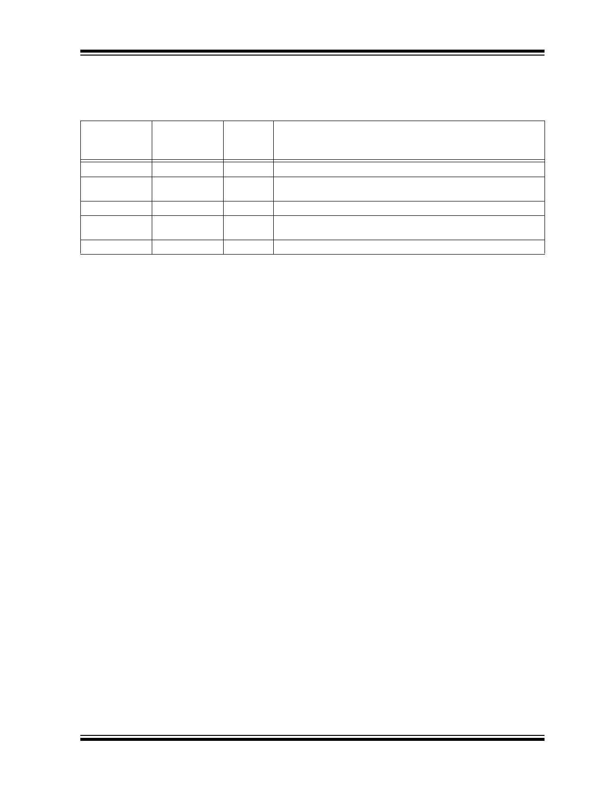
TABLE 1-1:
ELECTRICAL CHARACTERISTICS
Electrical Characteristics:
V
IN
= V
BAT
+ 1.0V; C
OUT
= 4.7 μF, I
OUT
= 100 μA; T
J
= +25°C, bold values indicate
–40°C ≤ T
J
≤ +125°C; unless noted.
Parameter
Symbol
Min.
Typ.
Max.
Units
Conditions
Battery Voltage Accuracy
V
BAT
–0.75
—
0.75
%
Variation from nominal V
OUT
, –5°C
to +60°C
Battery Voltage Temperature
Coefficient
∆V
BAT
/
∆T
—
40
—
ppm/°C
Note 1
Line Regulation
∆V
BAT
/
V
BAT
—
0.009
0.05
%/V
V
IN
= V
BAT
+ 1V to 16V
—
—
0.1
Load Regulation
∆V
BAT
/
V
BAT
—
0.05
0.5
%
I
OUT
= 100 μA to 500 mA,
Note 2
—
—
0.7
Dropout Voltage (
Note 3
)
V
IN
–
V
BAT
—
380
500
mV
I
OUT
= 500 mA
—
—
600
Ground Pin Current (
Note 4
,
Note 5
)
I
GND
—
85
130
µA
V
EN
≥ 3.0V, I
OUT
= 100 μA
—
—
170
—
11
20
mA
V
EN
≥ 3.0V, I
OUT
= 500 mA
—
—
25
Ground Pin Quiescent
Current (
Note 5
)
I
GND
—
0.05
3
µA
V
EN
≤ 0.4V (shutdown)
—
0.10
8
V
EN
≤ 0.18V (shutdown)
Ripple Rejection
PSRR
—
75
—
dB
f = 120 Hz
Current Limit
I
LIMIT
—
750
900
mA
V
BAT
= 0V
—
—
1000
Thermal Regulation
∆V
BAT
/
∆P
D
—
0.05
—
%/W
Note 6
ENABLE Input
Enable Input Logic-Low
Voltage
V
ENL
—
0.4
—
V
V
EN
= logic-low (shutdown)
—
—
0.18
2.0
—
—
V
EN
= logic-high (enabled)
MIC79050
DS20005771A-page 4
2017 Microchip Technology Inc.
Enable Input Current
I
ENL
—
0.01
–1
µA
V
ENL
≤ 0.4V (shutdown)
—
0.01
–2
V
ENL
≤ 0.18V (shutdown)
—
I
ENH
—
5
20
µA
V
ENH
≥ 2.0V (enabled)
—
—
25
Note 1:
Battery voltage temperature coefficient is the worst case voltage change divided by the total temperature
range.
2:
Regulation is measured at constant junction temperature using low duty cycle pulse testing. Parts are
tested for load regulation in the load range from 100 μA to 500 mA. Changes in output voltage due to heat-
ing effects are covered by the thermal regulation specification.
3:
Dropout voltage is defined as the input to battery output differential at which the battery voltage drops 2%
below its nominal value measured at 1V differential.
4:
Ground pin current is the charger quiescent current plus pass transistor base current. The total current
drawn from the supply is the sum of the load current plus the ground pin current.
5:
V
EN
is the voltage externally applied to devices with the EN (enable) input pin. MSOP-8 (MM) and SOIC-8
(M) packages only.
6:
Thermal regulation is the change in battery voltage at a time “t” after a change in power dissipation is
applied, excluding load or line regulation effects. Specifications are for a 500 mA load pulse at V
IN
= 16V
for t = 10 ms.
TABLE 1-1:
ELECTRICAL CHARACTERISTICS (CONTINUED)
Electrical Characteristics:
V
IN
= V
BAT
+ 1.0V; C
OUT
= 4.7 μF, I
OUT
= 100 μA; T
J
= +25°C, bold values indicate
–40°C ≤ T
J
≤ +125°C; unless noted.
Parameter
Symbol
Min.
Typ.
Max.
Units
Conditions
2017 Microchip Technology Inc.
DS20005771A-page 5
MIC79050
TEMPERATURE SPECIFICATIONS (
Note 1
)
Parameters
Sym.
Min.
Typ.
Max.
Units
Conditions
Temperature Ranges
Junction Operating Temperature
Range
T
J
–40
—
+125
°C
—
Storage Temperature Range
T
S
–65
—
+150
°C
—
Lead Temperature
—
—
—
+260
°C
Soldering, 5s
Package Thermal Resistances (
Note 2
)
Thermal Resistance MSOP-8
JA
—
80
—
°C/W
—
Thermal Resistance SOIC-8
JA
—
63
—
°C/W
—
Thermal Resistance SOT-223
JC
—
15
—
°C/W
—
JA
—
62
—
°C/W
—
Note 1:
The maximum allowable power dissipation is a function of ambient temperature, the maximum allowable
junction temperature and the thermal resistance from junction to air (i.e., T
A
, T
J
,
JA
). Exceeding the
maximum allowable power dissipation will cause the device operating junction temperature to exceed the
maximum +125°C rating. Sustained junction temperatures above +125°C can impact the device reliability.
2:
The maximum allowable power dissipation at any T
A
(ambient temperature) is calculated using: P
D(max)
=
(T
J(max)
– T
A
) ÷ θ
JA
. Exceeding the maximum allowable power dissipation will result in excessive die tem-
perature, and the regulator will go into thermal shutdown.
MIC79050
DS20005771A-page 6
2017 Microchip Technology Inc.
2.0
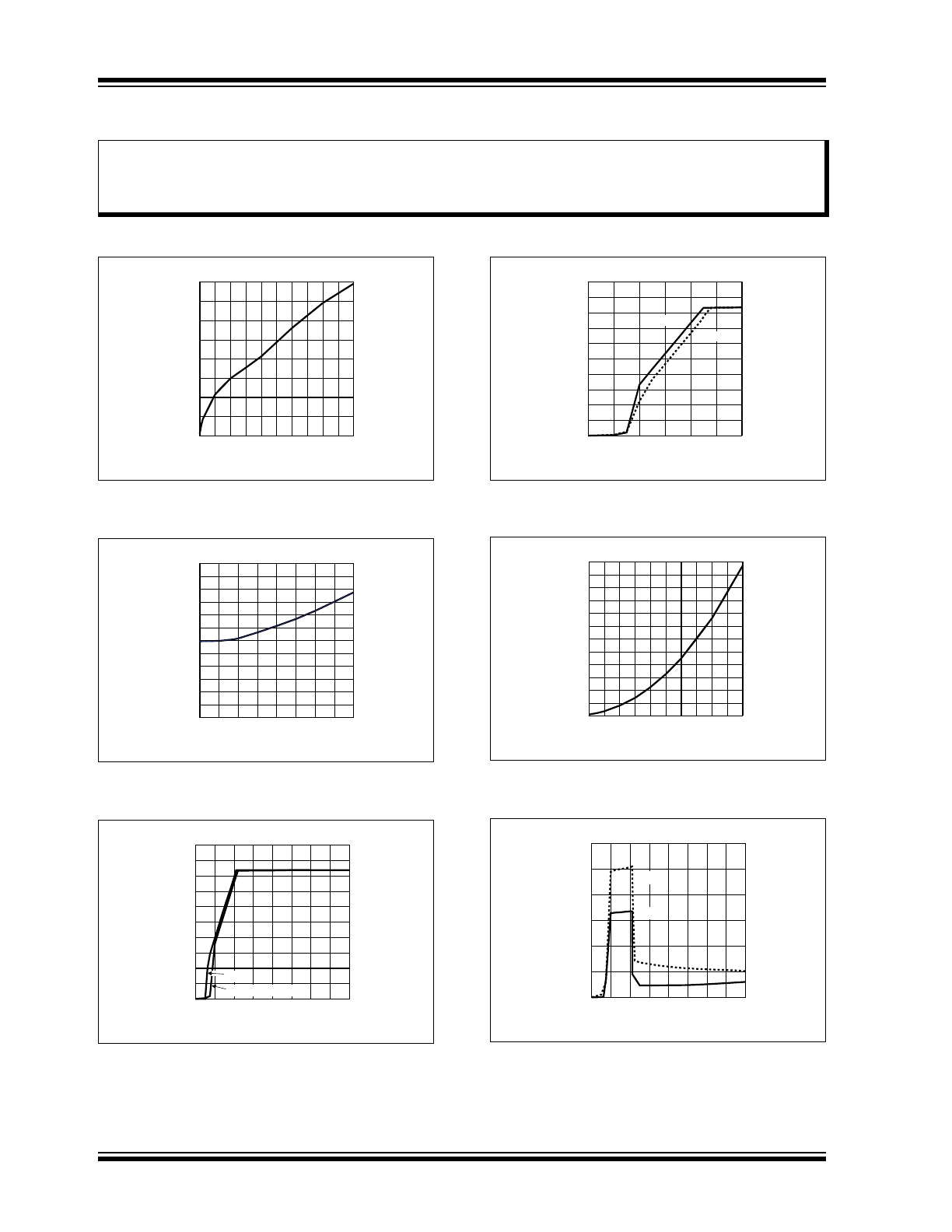
TYPICAL PERFORMANCE CURVES
FIGURE 2-1:
Dropout Voltage vs. Output
Current.
FIGURE 2-2:
Dropout Voltage vs.
Temperature.
FIGURE 2-3:
Dropout Characteristics.
FIGURE 2-4:
Dropout Characteristics.
FIGURE 2-5:
Output Current vs. Ground
Current.
FIGURE 2-6:
Ground Current vs. Supply
Voltage.
Note:
The graphs and tables provided following this note are a statistical summary based on a limited number of
samples and are provided for informational purposes only. The performance characteristics listed herein
are not tested or guaranteed. In some graphs or tables, the data presented may be outside the specified
operating range (e.g., outside specified power supply range) and therefore outside the warranted range.
0
100
200
300
400
0
100
200
300
400
500
DROPOUT VOLTAGE (mV)
OUTPUT CURRENT (mA)
0
100
200
300
400
500
600
-40
0
40
80
120
DROPOUT VOLTAGE (mV)
TEMPERATURE (°C)
0
1
2
3
4
5
0
2
4
6
8
10 12 14 16
OUTPUT VOLTAGE (V)
INPUT VOLTAGE (V)
50mA, 150mA
5mA
0
1
2
3
4
5
0
2
4
6
OUTPUT VOLTAGE (V)
INPUT VOLTAGE (V)
250mA
500mA
0
2
4
6
8
10
12
0
100
200
300
400
500
GROUND CURRENT (mA)
OUTPUT CURRENT (mA)
0
0.5
1
1.5
0
4
8
12
16
GROUND CURRENT (mA)
SUPPLY VOLTAGE (V)
50mA
5mA
2017 Microchip Technology Inc.
DS20005771A-page 7
MIC79050
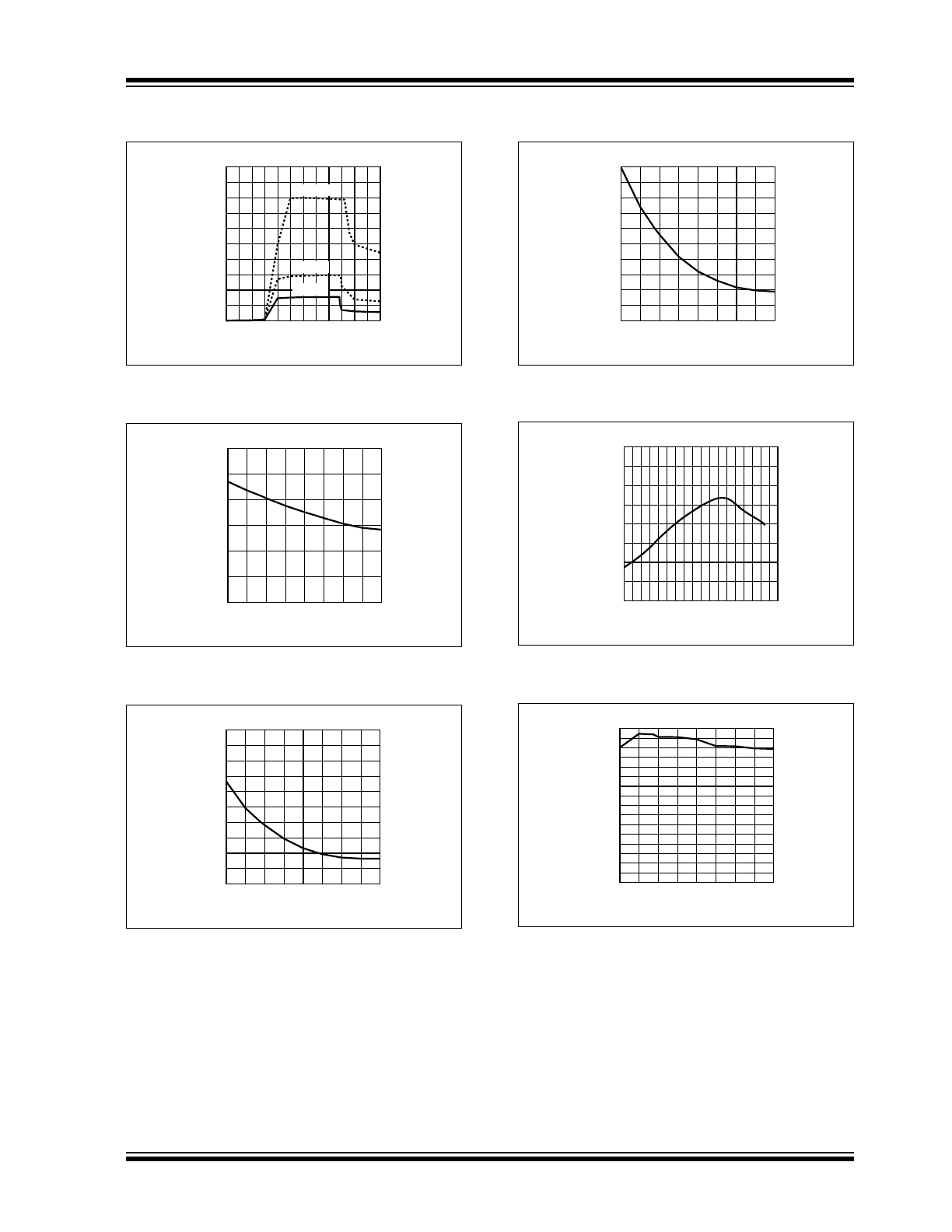
FIGURE 2-7:
Ground Current vs. Supply
Voltage.
FIGURE 2-8:
Ground Current vs.
Temperature.
FIGURE 2-9:
Ground Current vs.
Temperature.
FIGURE 2-10:
Ground Current vs.
Temperature.
FIGURE 2-11:
Battery Voltage vs.
Temperature.
FIGURE 2-12:
Short-Circuit Current vs.
Temperature.
0
5
10
15
20
25
0
1
2
3
4
5
6
GROUND CURRENT (mA)
SUPPLY VOLTAGE (V)
500mA
250mA
125mA
0
50
100
150
-40
0
40
80
120
GROUND CURRENT (μA)
TEMPERATURE (°C)
3.0
3.2
3.4
3.6
3.8
4.0
-40
0
40
80
120
GROUND CURRENT (mA)
TEMPERATURE (°C)
11.0
11.5
12.0
12.5
13.0
13.5
-40
0
40
80
120
GROUND CURRENT (mA)
TEMPERATURE (°C)
4.190
4.195
4.200
4.205
4.210
-40 -20 0 20 40 60 80 100120140
OUTPUT VOLTAGE (V)
TEMPERATURE (°C)
0
100
200
300
400
500
600
700
800
-40
0
40
80
120
SHORT CIRCUIT CURRENT (mA)
TEMPERATURE (°C)
MIC79050
DS20005771A-page 8
2017 Microchip Technology Inc.
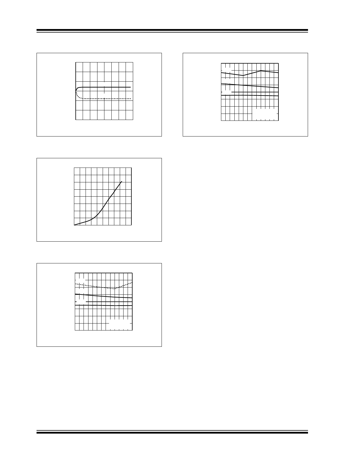
FIGURE 2-13:
Typical Voltage Drift Limits
vs. Time
.
FIGURE 2-14:
Reverse Leakage Current
vs. Output Voltage
.
FIGURE 2-15:
Reverse Leakage Current
vs. Output Voltage.
FIGURE 2-16:
Reverse Leakage Current
vs. Temperature.
-0.75
-0.25
0.25
0.75
0
200
400
600
800
DRIFT FROM NOMINAL VOUT (%)
TIME (hrs)
Upper
Lower
0
5
10
15
20
0
1
2
3
4
5
REVERSE LEAKAGE CURRENT (μA)
OUTPUT VOLTAGE (V)
0
5
10
15
20
-5
5
15
25
35
45
55
REVERSE LEAKAGE CURRENT (μA)
TEMPERATURE (°C)
3.0V
3.6V
4.2V
V
IN
+V
E N
FLOATING
0
5
10
15
20
-5
5
15
25
35
45
55
REVERSE LEAKAGE CURRENT (μA)
TEMPERATURE (°C)
3.0V
3.6V
4.2V
V
IN
+V
E N
GROUNDED
2017 Microchip Technology Inc.
DS20005771A-page 9
MIC79050
3.0
PIN DESCRIPTIONS
The descriptions of the pins are listed in
Table 3-1
.
TABLE 3-1:
PIN FUNCTION TABLE
Pin Number
SOT-223
Pin Number
SOIC-8,
MSOP-8
Pin Name
Description
1
2
IN
Supply input.
2, TAB
5, 6, 7, 8
GND
Ground: SOT-223 pin 2 and TAB are internally connected. SOIC-8
pins 5 through 8 are internally connected.
3
3
BAT
Battery voltage output.
—
1
EN
Enable (Input): TTL/CMOS-compatible control input. Logic-high =
enable; logic-low or open = shutdown.
—
4
FB
Feedback node.

MIC79050
DS20005771A-page 10
2017 Microchip Technology Inc.
4.0
FUNCTIONAL DESCRIPTION
The MIC79050 is a high-accuracy, linear battery
charging circuit designed for the simplest
implementation of a single lithium-ion (Li-ion) battery
charger. The part can operate from a regulated or
unregulated power source, making it ideal for various
applications. The MIC79050 can take an unregulated
voltage source and provide an extremely accurate
termination voltage. The output voltage varies only
0.75% from nominal over the standard temperature
range for Li-ion battery charging (–5°C to +60°C). With
a minimum of external components, an accurate
constant-current charger can be designed to provide
constant-current, constant-voltage charging for Li-ion
cells.
4.1
Input Voltage
The MIC79050 can operate with an input voltage up to
16V (20V absolute maximum), ideal for applications
where the input voltage can float high, such as an
unregulated wall adapter that obeys a load-line. Higher
voltages can be sustained without any performance
degradation to the output voltage. The line regulation of
the device is typically 0.009%/V; that is, a 10V change
on the input voltage corresponds to a 0.09% change in
output voltage.
4.2
Enable
The MIC79050 has an enable pin that allows the
charger to be disabled when the battery is fully charged
and the current drawn by the battery has approached a
minimum and/or the maximum charging time has timed
out. When disabled, the regulator output sinks a
minimum of current with the battery voltage applied
directly onto the output. This current is typically 12 μA
or less.
4.3
Feedback
The feedback pin allows for external manipulation of
the control loop. This node is connected to an external
resistive divider network, which is connected to the
internal error amplifier. This amplifier compares the
voltage at the feedback pin to an internal voltage
reference. The loop then corrects for changes in load
current or input voltage by monitoring the output
voltage and linearly controlling the drive to the large,
PNP pass element. By externally controlling the
voltage at the feedback pin the output can be disabled
or forced to the input voltage. Pulling and holding the
feedback pin low forces the output low. Holding the
feedback pin high forces the pass element into
saturation, where the output will be the input minus the
saturation (dropout) voltage.
4.4
Battery Output
The BAT pin is the output of the MIC79050 and
connects directly to the cell to provide charging current
and voltage. When the input is left floating or grounded,
the BAT pin limits reverse current to <12 μA to minimize
battery drain.