

2013 - 2016 Microchip Technology Inc.
DS00001561C-page 1
General Description
The SEC1110 and SEC1210 provide a single-chip
solution for a Smart Card bridge to USB and UART
interfaces. These bridges are controlled by an
enhanced 8051 micro controller and all chip peripher-
als are accessed and controlled through the SFR or
XDATA register space. TrustSpan
TM
Technology
enables digital systems to securely communicate, pro-
cess, move and store information on system boards,
across networks and through the cloud.
Feature Highlights
• Smart Card
- The SEC1110 provides one Smart Card inter-
face and the SEC1210 provides two
- Fully compliant with ISO/IEC 7816, EMV 4.2/
4.3, ETSI TS 102 221 and PC/SC standards
- Versatile ETU rate generation, supporting
current and proposed rates (up to 826 Kbps)
- Full support of both T=0 and T=1 protocols
- Full-packet FIFO (261 bytes), for transmit
and receive
- Half-duplex operation (no software interven-
tion required between transmit and receive
phases of exchange)
- Loose real-time response required of soft-
ware (approximately 180 ms)
- Dynamically programmable FIFO threshold
with byte granularity
- Time-out FIFO flush interrupt, independent of
threshold
- Programmable Smart Card clock frequency
- UART-like register file structure
- Supports Class A, Class B, Class C, or Class
AB Smart Cards (1.8 V, 3.0 V and 5.0 V
cards)
- Automatic character repetition for T=0 proto-
col parity error recovery
- Automatic card deactivation on card removal
and on other system events, including per-
sistent parity errors
- Internal procedure byte filtering for T=0 proto-
col
- Protocol timers (Guard, Timeout, and CWT)
for EMV-defined timing parameters
–Detection of an unresponsive card
–Activation/deactivation sequences
–Cold/warm resets
–Monitoring for all EMV timing constraints
–16-bit general purpose down counter for software
timing use
- Fully compliant ESD protection on card pins
• USB
- 12 Mbps USB operation compliant to the
USB 2.0 Specification
- Integrated USB 1.5 K pull-up resistor and
Dp,Dm series termination resistors
- Integrated USB devices controller with:
–8/16/32/64 byte control buffer
–Five 8/16/32/64 byte programmable (bulk/
interrupt) endpoint buffers
• 8051 Processor
- Reduced instruction cycle time (approxi-
mately 9 times 80C51)
- 9.6 MHz max clock speed
- Enhanced peripherals; three 16-bit timers,
watchdog timer, interrupt controller, JTAG
- OTP (One Time Programmable)
ROM : 16 KB RAM : 1.5 KB
• Boot ROM : 16 KB UART (SEC1210 only)
—
Standard PC baud rates supported
—
3 M baud high-speed rate (not PC standard)
• SPI (SEC1210 only)
- Master capability with 12 MHz max perfor-
mance
• General
- 5.0 V tolerance on user accessible IO pins
- Self-clocking internal oscillator, no external
crystal required
- 3.6 V - 5.5 V supply input
–Internal 4.8 V comparator disables Class A card
support if the input voltage is too low
- Available in commercial (0ºC to +70ºC) and
industrial (-40ºC to +85ºC) temperature
ranges
Applications
• USB Smart Card reader
• UART-based Smart Card reader
• Dual Smart Card reader
SEC1110/SEC1210
Smart Card Bridge to USB and UART Interfaces

SEC1110/SEC1210
DS00001561C-page 2
2013 - 2016 Microchip Technology Inc.
TO OUR VALUED CUSTOMERS
It is our intention to provide our valued customers with the best documentation possible to ensure successful use of your Microchip
products. To this end, we will continue to improve our publications to better suit your needs. Our publications will be refined and
enhanced as new volumes and updates are introduced.
If you have any questions or comments regarding this publication, please contact the Marketing Communications Department via
E-mail at
docerrors@microchip.com
. We welcome your feedback.
Most Current Data Sheet
To obtain the most up-to-date version of this data sheet, please register at our Worldwide Web site at:
http://www.microchip.com
You can determine the version of a data sheet by examining its literature number found on the bottom outside corner of any page.
The last character of the literature number is the version number, (e.g., DS30000000A is version A of document DS30000000).
Errata
An errata sheet, describing minor operational differences from the data sheet and recommended workarounds, may exist for cur-
rent devices. As device/documentation issues become known to us, we will publish an errata sheet. The errata will specify the
revision of silicon and revision of document to which it applies.
To determine if an errata sheet exists for a particular device, please check with one of the following:
• Microchip’s Worldwide Web site;
http://www.microchip.com
• Your local Microchip sales office (see last page)
When contacting a sales office, please specify which device, revision of silicon and data sheet (include -literature number) you are
using.
Customer Notification System
Register on our web site at
www.microchip.com
to receive the most current information on all of our products.

2013 - 2016 Microchip Technology Inc.
DS00001561C-page 3
SEC1110/SEC1210
Table of Contents
1.0 Introduction ..................................................................................................................................................................................... 4
2.0 Block Diagrams ............................................................................................................................................................................... 7
3.0 Pin Table ......................................................................................................................................................................................... 9
4.0 Pin Configurations ......................................................................................................................................................................... 11
5.0 Pin Descriptions ............................................................................................................................................................................ 13
6.0 Pin Reset States ........................................................................................................................................................................... 16
7.0 8051 Embedded Controller ........................................................................................................................................................... 19
8.0 EC External Interrupts ................................................................................................................................................................... 24
9.0 8051 Special Function Registers .................................................................................................................................................. 27
10.0 Smart Card Interface ................................................................................................................................................................... 46
11.0 USB Controller Description ......................................................................................................................................................... 92
12.0 GPIO and LED Interface ........................................................................................................................................................... 117
13.0 Two Pin Serial Port (UART) ...................................................................................................................................................... 132
14.0 Serial Peripheral Interconnect (SPI1) - Master ......................................................................................................................... 145
15.0 Clock and Reset ........................................................................................................................................................................ 150
16.0 OTP ROM Test Interface .......................................................................................................................................................... 176
17.0 TEST Modes, JTAG, and XNOR .............................................................................................................................................. 187
18.0 DC Parameters ......................................................................................................................................................................... 188
19.0 8051 Timers .............................................................................................................................................................................. 196
20.0 Timing Diagrams ....................................................................................................................................................................... 205
21.0 Package Outlines
................................................................................................................................................................................................. 207
Appendix A: Acronyms, Definitions and Conventions ....................................................................................................................... 209
Appendix B: References ................................................................................................................................................................... 212
Appendix C: Revision History ........................................................................................................................................................... 213
The Microchip Web Site .................................................................................................................................................................... 214
Customer Change Notification Service ............................................................................................................................................. 214
Customer Support ............................................................................................................................................................................. 214
Product Identification System ........................................................................................................................................................... 215

SEC1110/SEC1210
DS00001561C-page 4
2013 - 2016 Microchip Technology Inc.
1.0
INTRODUCTION
The SEC1110 and SEC1210 provide a single-chip solution for a Smart Card bridge to USB and UART interfaces. These
bridges are controlled by an enhanced 8051 micro controller and all chip peripherals are accessed and controlled
through the SFR or XDATA register space.
1.1
Features
• Smart Card
- Fully compliant with standards: ISO/IEC 7816, EMV 4.2/4.3, ETSI TS 102 221 and PC/SC
- Versatile ETU rate generation, supporting current and proposed rates (to 826 Kbps and beyond)
- Full support of both T=0 and T=1 protocols
- Full-packet FIFO (261 bytes), for transmit and receive
- Half-duplex operation, with no software intervention required between Transmit and Receive phases of an
exchange
- Very loose real-time response required of software: approximately 180 ms worst case
- Dynamically programmable FIFO threshold, with byte granularity
- Time-out FIFO flush interrupt, independent of threshold
- Programmable Smart Card clock frequency
- UART-like register file structure
- Supports Class A, Class B, Class C, or Class AB Smart Cards (all 1.8 V, 3.0 V and 5.0 V cards)
- Automatic character repetition for T=0 protocol parity error recovery
- Automatic card deactivation on card removal and on other system events, including persistent parity errors
- Internal procedure byte filtering for T=0 protocol
- Protocol timers (guard, time-out and CWT) for EMV-defined timing parameters
- Detection of an unresponsive card
- Activation/deactivation sequences
- Cold/warm resets
- Monitoring for all EMV timing constraints
- 16-bit general purpose down counter for software timing use
- Fully compliant ESD protection on card pins per JESD22-A114D (March 2006) and JESD22-A115A “Machine
Model” from AN1181
- Fully EMV compliant, internal signal current limits
- 3.3 V internal operation with 5.0 V tolerant buffers where required
- Self-contained management of Smart Card power:
- SC1_VCC and SC2_VCC, supply output
- Regulator for 1.8 V, 3.0 V, and 5.0 V from supply input
- Current limiter with over-current sense interrupt (short circuit detect)
- Hardware-ensured, compliant deactivation sequence on card removal
- Synchronous card support
• USB
- 12 Mbps USB operation compliant with the USB 2.0 Specification
- Integrated USB 1.5 K pull-up resistor
- Integrated Series resistors on USB_DP, USB_DM
- Integrated USB devices controller with:
- 8/16/32/64 byte control endpoint 0 buffer
- Five 8/16/32/64 byte programmable (bulk/interrupt) endpoint buffers
• 8051
- Reduced instruction cycle time (approximately 9 times 80C51)
- 9.6 MHz max clock speed
- Enhanced peripherals: two 16-bit timers, watch dog timer, interrupt controller, JTAG
- 16 KB One Time Programmable (OTP) ROM
- 1.5 KB RAM
- 4 KB (SEC1100/SEC1200)/ 16KB (SEC1110/SEC1210) ROM

2013 - 2016 Microchip Technology Inc.
DS00001561C-page 5
SEC1110/SEC1210
• UART
- Standard PC (9600, 19200, 38400 and 115200) baud rates supported
- 3 M baud high-speed rate (non-PC standard)
• SPI
- Master capability with 12 MHz max performance
• General
- 5.0 V tolerance on user accessible IO pins
- Self-clocking internal oscillator, no external crystal required
- 3.6 V-5.5 V supply input
- Internal 4.8 V
comparator disables Class A card support if the input voltage is too low
1.2
Smart Card Subsystem
The SEC1110 and SEC1210 are fully compliant with the prevailing Smart Card standards: ISO7816, EMV, and PC/SC.
It meets and exceeds all existing requirements for communication bit rate (ETU duration) and includes support for pro-
posed bit rates up to 826 Kbps. Signal levels and current limits are also fully compliant.
The Smart Card power is regulated and switched internally, supporting all 5.0 V, 3.0 V, and 1.8 V Smart Cards (classes
A, B, and C, respectively). Over-current protection is provided, and a detected over-current condition is available as an
interrupt. The required standard activation and deactivation sequences are provided with software interaction. However,
deactivation is handled in hardware as the card is being removed. This scenario ensures the required sequence regard-
less of software participation. If the system clock is inactive at the time, the card movement is detected asynchronously,
and the Wake-On Event feature is used to re-start the system clock so that the de-activation sequence can continue.
Interface signals to the Smart Card are designed to meet both standard drive levels and current limitations internally,
requiring no external series resistors. ESD protection on these signals meets the full standard requirements.
The device is a superset of the familiar 16450 UART architecture, with extensions in the form of a larger FIFO, special-
ized state machines for T=0 protocol parsing, automatic half-duplex turnaround at the completion of a transmitted mes-
sage, and a specially-designed set of timers to enforce standards compliance in timing (as required of a terminal by the
ISO7816 and EMV standards).
With the full-packet-depth FIFO on-chip, software is almost totally excluded from real-time requirements. It loads an out-
going message into the FIFO, triggers the transfer, and reads the returned data at any time after it becomes available.
The reset sequence (cold or warm) is equally hands-off: software sets up the sequence and activates the reset, and is
alerted when the ATR message has been received (via the FIFO Threshold Interrupt). The threshold is dynamically pro-
grammable with byte granularity, so that threshold interrupts can be received at various stages in the processing of a
message of initially unknown length (such as ATR).
For detecting data time-outs, and for other mandatory timing tasks having to do with communication with a Smart Card,
a set of three protocol timers is provided:
• Time-out timer, for monitoring the standard WWT, BWT and WTX time-out intervals
• CWT timer, for monitoring the T=1 CWT time-out interval
• Guard timer, for ensuring the BGT and EGT transmission intervals, with special usage during a Reset sequence.
A separate general purpose timer is provided for software driver use.
Synchronous card support using GPIOs controlled via registers in the Smart Card device.
SEC1110/SEC1210
DS00001561C-page 6
2013 - 2016 Microchip Technology Inc.
1.3
USB Subsystem
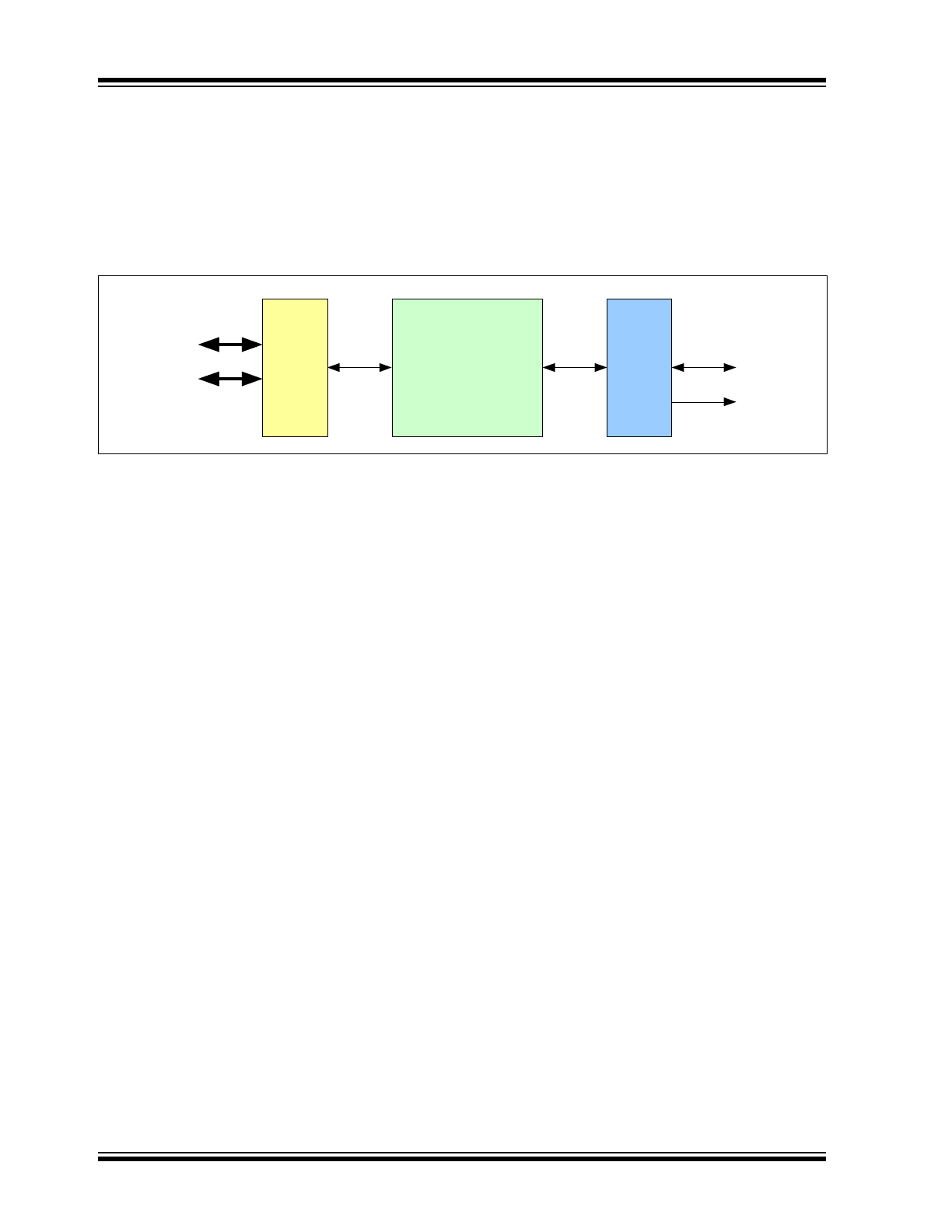
The USB Subsystem is made up of the following 3 functional blocks
• FS USB PHY
• USB Device Controller (UDC)
• Interface Bridge with USB endpoint buffers
1.3.1
FS USB PHY AND DEVICE CONTROLLER
The FS USB PHY contains the D+ pull-up resistor and handles the reception of USB data. The D+ and D- signals are
passed through the differential receiver (which is external to the device controller core) to get a single-ended bit stream.
The device controller has a digital phase-locked loop (DPLL) to extract the clock and data information. The clock and
data are passed to the SIE (serial interface engine) block to identify the sync pattern and for NRZI-NRZ conversion. This
NRZ data is then passed through a bit-stripper which strips off excessive inserted zeros. The data stream is passed
through a PID decoder and checker to identify different PID’s. The SIE block handles the protocol according to the type
of PID and the endpoint to which the current transaction is addressed. If it is a data PID, the serial data is assembled
into byte format and the received data is CRC is checked, then put into a one-byte buffer. The protocol layer takes the
data from the buffer and forwards it to the Interface Bridge. On control transfers to endpoint 0, the protocol layer forwards
the transfers to the endpoint block. If the application violates the data transfer protocol during the transfer of data from
the buffer to the application bus, the protocol layer controls the SIE to recover from this error.
1.3.2
INTERFACE BRIDGE AND ENDPOINT BUFFERS
These act as the interface between the 8051 micro controller and the USB device controller. The USB endpoint buffers
are memory mapped on the 8051 XDATA bus. A simple buffer scheme is employed, which assigns a single/ping-pong
buffer to each USB endpoint for ease of software control. Each buffer must be cleared before the next data transfer can
be started.
When USB OUT data is received, it is placed into the appropriate OUT endpoint buffer and the 8051 is signaled with an
interrupt (polling is also available)
When an IN request is received, the 8051 is signaled with an interrupt and the 8051 will transfer data to the appropriate
IN endpoint buffer and set a ready flag. The data will automatically be encoded for transfer over the USB bus.
1.4
Power Management Unit
The programmable clock divider supports division of the 48 MHz main clock. Additionally it enables power down under
program or hardware control. Exit from power down is accomplished through a single input pin. The power management
methods employed will enable a USB Suspend current of 200
A typical (400 A typical including Rpu current). In STOP
Mode, 1
A is the maximum current for a bare bones design.
FIGURE 1-1:
USB SUBSYSTEM BLOCK
USB
FS
PHY
USB 1.1
Device Controller
Interface
Bridge
+
Endpoint
Buffers
USB D+
USB D-
XDATA
Interrupt
2013 - 2016 Microchip Technology Inc.
DS00001561C-page 7
SEC1110/SEC1210
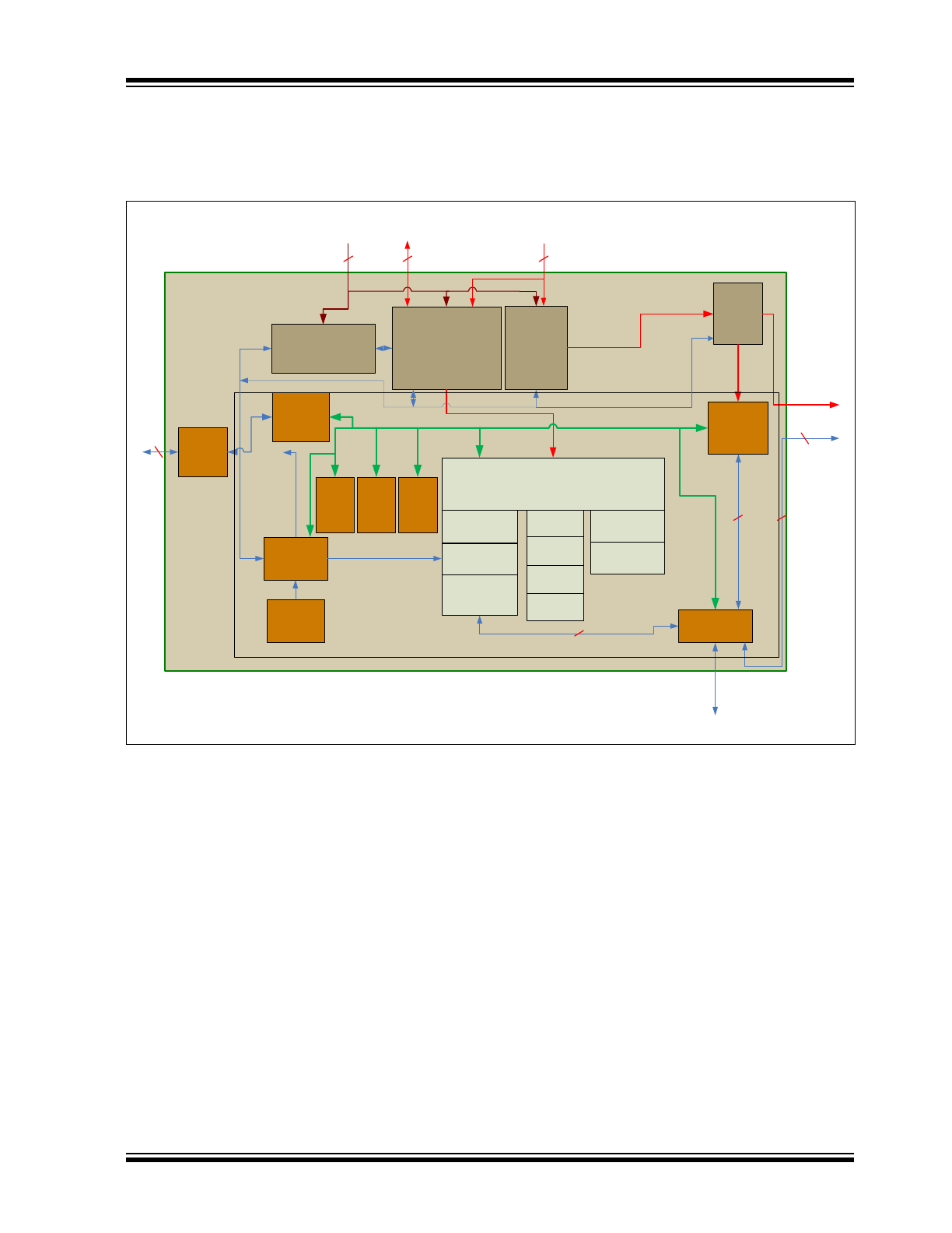
2.0
BLOCK DIAGRAMS
FIGURE 2-1:
SEC1110 BLOCK DIAGRAM
3.0 V - 5.5 V or VBUS
Smart
Card
Regulators
5.0 V
3.0 V
1.8 V
16
KB
OTP
ROM
1.5
KB
RAM
USB
PHY
CLK_PWR
USB
Device
Controller
ISO7816 /
Smart
Card
Interface
Smart
Card
Power
Control
Power On Reset
Power Fail Detect
Reset
8051
CPU
256 x 8
RAM
On Chip
Debug
JTAG
Timer 0
Timer 1
Watchdog
Timer
External
Interrupts
CPU Clock
Management
CPU Power
Management
USB/GPIO/Core
Regulators
3.3 V
1.2 V
4
XDATA
48 MHz
Oscillator
GPIO
Smart Card 1
7 pins
Miscellaneous
D+
D-
VDD33
1
1
1
4
6
6
2
4/16
KB
ROM
Timer 2
SEC1110/SEC1210
DS00001561C-page 8
2013 - 2016 Microchip Technology Inc.
FIGURE 2-2:
SEC1210 BLOCK DIAGRAM
3.0 V - 5.5 V or VBUS
Smart
Card
Regulators
5.0 V
3.0 V
1.8 V
16
KB
OTP
ROM
1.5 KB
RAM
USB
PHY
CLK_PWR
USB
Device
Controller
ISO7816 /
Smart
Card
Interface
Smart Card
Power
Control
Power On Reset
Power Fail Detect
Reset
8051
CPU
256 x 8
RAM
On Chip
Debug
JTAG
Timer 0
Timer 1
Watchdog
Timer
External
Interrupts
CPU Clock
Management
CPU Power
Management
USB/GPIO/Core
Regulators
3.3 V
1.2 V
XDATA
48 MHz
Oscillator
SPI1
UART
16550
GPIO
Smart Card1
7 pins
1
Miscellaneous
D+
D-
Smart
Card
Regulators
5.0 V
3.0 V
1.8 V
Smart Card
Power
Control
SAM2
4
VDD33
1
1
1
4
4
6
1
3
2
8
6
6 + 3
Timer 2
4/16
KB
OTP
ROM
2013 - 2016 Microchip Technology Inc.
DS00001561C-page 9
SEC1110/SEC1210
3.0
PIN TABLE
3.1
SEC1110 16-Pin QFN
3.2
SEC1210 24-Pin QFN
TABLE 3-1:
SEC1110 16-PIN PACKAGE
SMART CARD (7 PINS)
SC1_VCC
Sc1_rst_N
sc1_clk
sc1_io
SC1_C8
SC1_PRSNT_N/
JTAG_TMS
SC1_C4
USB INTERFACE (2 PINS)
USB_DP
usb_DM
MISC (5 PINS)
RESET_N
SC_LED_ACT_N/
JTAG_TDO
TEST
JTAG_CLK
JTAG_TDI
DIGITAL, POWER (2 PINS)
VDD33
VDD5
TOTAL 16 (VSS - THERMAL SLUG)
TABLE 3-2:
SEC1210 24-PIN PACKAGE
SMART CARD (7 PINS)
SC1_VCC
Sc1_rst_N
sc1_clk
sc1_io
SC1_C8
SC1_PRSNT_N/
JTAG_TMS
SC1_C4
SMART CARD 2/SECURITY AUTHENTICATION MODULE (5 PINS)
SC2_VCC
Sc2_rst_N
sc2_clk
sc2_io
SC2_PRSNT_N/
JTAG_TDI
USB INTERFACE (2 PINS)
USB_DP
usb_DM
SPI1/UART (4 PINS)
SPI1_MISO/RXD
SPI1_MOSI/TXD
SPI1_CLK/CTS_OUT
SPI1_CE/RTS_IN
MISC (4 PINS)
SEC1110/SEC1210
DS00001561C-page 10
2013 - 2016 Microchip Technology Inc.
RESET_N
SC_LED_ACT_N/
JTAG_TDO
TEST
JTAG_CLK
DIGITAL, POWER (2 PINS)
VDD33
VDD5
TOTAL 24 (VSS - THERMAL SLUG)
Note:
The NC pins are “No Connects”. There are no NC pads in the Known Good Die (KGD).
TABLE 3-2:
SEC1210 24-PIN PACKAGE
2013 - 2016 Microchip Technology Inc.
DS00001561C-page 1
General Description
The SEC1110 and SEC1210 provide a single-chip
solution for a Smart Card bridge to USB and UART
interfaces. These bridges are controlled by an
enhanced 8051 micro controller and all chip peripher-
als are accessed and controlled through the SFR or
XDATA register space. TrustSpan
TM
Technology
enables digital systems to securely communicate, pro-
cess, move and store information on system boards,
across networks and through the cloud.
Feature Highlights
• Smart Card
- The SEC1110 provides one Smart Card inter-
face and the SEC1210 provides two
- Fully compliant with ISO/IEC 7816, EMV 4.2/
4.3, ETSI TS 102 221 and PC/SC standards
- Versatile ETU rate generation, supporting
current and proposed rates (up to 826 Kbps)
- Full support of both T=0 and T=1 protocols
- Full-packet FIFO (261 bytes), for transmit
and receive
- Half-duplex operation (no software interven-
tion required between transmit and receive
phases of exchange)
- Loose real-time response required of soft-
ware (approximately 180 ms)
- Dynamically programmable FIFO threshold
with byte granularity
- Time-out FIFO flush interrupt, independent of
threshold
- Programmable Smart Card clock frequency
- UART-like register file structure
- Supports Class A, Class B, Class C, or Class
AB Smart Cards (1.8 V, 3.0 V and 5.0 V
cards)
- Automatic character repetition for T=0 proto-
col parity error recovery
- Automatic card deactivation on card removal
and on other system events, including per-
sistent parity errors
- Internal procedure byte filtering for T=0 proto-
col
- Protocol timers (Guard, Timeout, and CWT)
for EMV-defined timing parameters
–Detection of an unresponsive card
–Activation/deactivation sequences
–Cold/warm resets
–Monitoring for all EMV timing constraints
–16-bit general purpose down counter for software
timing use
- Fully compliant ESD protection on card pins
• USB
- 12 Mbps USB operation compliant to the
USB 2.0 Specification
- Integrated USB 1.5 K pull-up resistor and
Dp,Dm series termination resistors
- Integrated USB devices controller with:
–8/16/32/64 byte control buffer
–Five 8/16/32/64 byte programmable (bulk/
interrupt) endpoint buffers
• 8051 Processor
- Reduced instruction cycle time (approxi-
mately 9 times 80C51)
- 9.6 MHz max clock speed
- Enhanced peripherals; three 16-bit timers,
watchdog timer, interrupt controller, JTAG
- OTP (One Time Programmable)
ROM : 16 KB RAM : 1.5 KB
• Boot ROM : 16 KB UART (SEC1210 only)
—
Standard PC baud rates supported
—
3 M baud high-speed rate (not PC standard)
• SPI (SEC1210 only)
- Master capability with 12 MHz max perfor-
mance
• General
- 5.0 V tolerance on user accessible IO pins
- Self-clocking internal oscillator, no external
crystal required
- 3.6 V - 5.5 V supply input
–Internal 4.8 V comparator disables Class A card
support if the input voltage is too low
- Available in commercial (0ºC to +70ºC) and
industrial (-40ºC to +85ºC) temperature
ranges
Applications
• USB Smart Card reader
• UART-based Smart Card reader
• Dual Smart Card reader
SEC1110/SEC1210
Smart Card Bridge to USB and UART Interfaces
SEC1110/SEC1210
DS00001561C-page 2
2013 - 2016 Microchip Technology Inc.
TO OUR VALUED CUSTOMERS
It is our intention to provide our valued customers with the best documentation possible to ensure successful use of your Microchip
products. To this end, we will continue to improve our publications to better suit your needs. Our publications will be refined and
enhanced as new volumes and updates are introduced.
If you have any questions or comments regarding this publication, please contact the Marketing Communications Department via
E-mail at
docerrors@microchip.com
. We welcome your feedback.
Most Current Data Sheet
To obtain the most up-to-date version of this data sheet, please register at our Worldwide Web site at:
http://www.microchip.com
You can determine the version of a data sheet by examining its literature number found on the bottom outside corner of any page.
The last character of the literature number is the version number, (e.g., DS30000000A is version A of document DS30000000).
Errata
An errata sheet, describing minor operational differences from the data sheet and recommended workarounds, may exist for cur-
rent devices. As device/documentation issues become known to us, we will publish an errata sheet. The errata will specify the
revision of silicon and revision of document to which it applies.
To determine if an errata sheet exists for a particular device, please check with one of the following:
• Microchip’s Worldwide Web site;
http://www.microchip.com
• Your local Microchip sales office (see last page)
When contacting a sales office, please specify which device, revision of silicon and data sheet (include -literature number) you are
using.
Customer Notification System
Register on our web site at
www.microchip.com
to receive the most current information on all of our products.
2013 - 2016 Microchip Technology Inc.
DS00001561C-page 3
SEC1110/SEC1210
Table of Contents
1.0 Introduction ..................................................................................................................................................................................... 4
2.0 Block Diagrams ............................................................................................................................................................................... 7
3.0 Pin Table ......................................................................................................................................................................................... 9
4.0 Pin Configurations ......................................................................................................................................................................... 11
5.0 Pin Descriptions ............................................................................................................................................................................ 13
6.0 Pin Reset States ........................................................................................................................................................................... 16
7.0 8051 Embedded Controller ........................................................................................................................................................... 19
8.0 EC External Interrupts ................................................................................................................................................................... 24
9.0 8051 Special Function Registers .................................................................................................................................................. 27
10.0 Smart Card Interface ................................................................................................................................................................... 46
11.0 USB Controller Description ......................................................................................................................................................... 92
12.0 GPIO and LED Interface ........................................................................................................................................................... 117
13.0 Two Pin Serial Port (UART) ...................................................................................................................................................... 132
14.0 Serial Peripheral Interconnect (SPI1) - Master ......................................................................................................................... 145
15.0 Clock and Reset ........................................................................................................................................................................ 150
16.0 OTP ROM Test Interface .......................................................................................................................................................... 176
17.0 TEST Modes, JTAG, and XNOR .............................................................................................................................................. 187
18.0 DC Parameters ......................................................................................................................................................................... 188
19.0 8051 Timers .............................................................................................................................................................................. 196
20.0 Timing Diagrams ....................................................................................................................................................................... 205
21.0 Package Outlines
................................................................................................................................................................................................. 207
Appendix A: Acronyms, Definitions and Conventions ....................................................................................................................... 209
Appendix B: References ................................................................................................................................................................... 212
Appendix C: Revision History ........................................................................................................................................................... 213
The Microchip Web Site .................................................................................................................................................................... 214
Customer Change Notification Service ............................................................................................................................................. 214
Customer Support ............................................................................................................................................................................. 214
Product Identification System ........................................................................................................................................................... 215
SEC1110/SEC1210
DS00001561C-page 4
2013 - 2016 Microchip Technology Inc.
1.0
INTRODUCTION
The SEC1110 and SEC1210 provide a single-chip solution for a Smart Card bridge to USB and UART interfaces. These
bridges are controlled by an enhanced 8051 micro controller and all chip peripherals are accessed and controlled
through the SFR or XDATA register space.
1.1
Features
• Smart Card
- Fully compliant with standards: ISO/IEC 7816, EMV 4.2/4.3, ETSI TS 102 221 and PC/SC
- Versatile ETU rate generation, supporting current and proposed rates (to 826 Kbps and beyond)
- Full support of both T=0 and T=1 protocols
- Full-packet FIFO (261 bytes), for transmit and receive
- Half-duplex operation, with no software intervention required between Transmit and Receive phases of an
exchange
- Very loose real-time response required of software: approximately 180 ms worst case
- Dynamically programmable FIFO threshold, with byte granularity
- Time-out FIFO flush interrupt, independent of threshold
- Programmable Smart Card clock frequency
- UART-like register file structure
- Supports Class A, Class B, Class C, or Class AB Smart Cards (all 1.8 V, 3.0 V and 5.0 V cards)
- Automatic character repetition for T=0 protocol parity error recovery
- Automatic card deactivation on card removal and on other system events, including persistent parity errors
- Internal procedure byte filtering for T=0 protocol
- Protocol timers (guard, time-out and CWT) for EMV-defined timing parameters
- Detection of an unresponsive card
- Activation/deactivation sequences
- Cold/warm resets
- Monitoring for all EMV timing constraints
- 16-bit general purpose down counter for software timing use
- Fully compliant ESD protection on card pins per JESD22-A114D (March 2006) and JESD22-A115A “Machine
Model” from AN1181
- Fully EMV compliant, internal signal current limits
- 3.3 V internal operation with 5.0 V tolerant buffers where required
- Self-contained management of Smart Card power:
- SC1_VCC and SC2_VCC, supply output
- Regulator for 1.8 V, 3.0 V, and 5.0 V from supply input
- Current limiter with over-current sense interrupt (short circuit detect)
- Hardware-ensured, compliant deactivation sequence on card removal
- Synchronous card support
• USB
- 12 Mbps USB operation compliant with the USB 2.0 Specification
- Integrated USB 1.5 K pull-up resistor
- Integrated Series resistors on USB_DP, USB_DM
- Integrated USB devices controller with:
- 8/16/32/64 byte control endpoint 0 buffer
- Five 8/16/32/64 byte programmable (bulk/interrupt) endpoint buffers
• 8051
- Reduced instruction cycle time (approximately 9 times 80C51)
- 9.6 MHz max clock speed
- Enhanced peripherals: two 16-bit timers, watch dog timer, interrupt controller, JTAG
- 16 KB One Time Programmable (OTP) ROM
- 1.5 KB RAM
- 4 KB (SEC1100/SEC1200)/ 16KB (SEC1110/SEC1210) ROM
2013 - 2016 Microchip Technology Inc.
DS00001561C-page 5
SEC1110/SEC1210
• UART
- Standard PC (9600, 19200, 38400 and 115200) baud rates supported
- 3 M baud high-speed rate (non-PC standard)
• SPI
- Master capability with 12 MHz max performance
• General
- 5.0 V tolerance on user accessible IO pins
- Self-clocking internal oscillator, no external crystal required
- 3.6 V-5.5 V supply input
- Internal 4.8 V
comparator disables Class A card support if the input voltage is too low
1.2
Smart Card Subsystem
The SEC1110 and SEC1210 are fully compliant with the prevailing Smart Card standards: ISO7816, EMV, and PC/SC.
It meets and exceeds all existing requirements for communication bit rate (ETU duration) and includes support for pro-
posed bit rates up to 826 Kbps. Signal levels and current limits are also fully compliant.
The Smart Card power is regulated and switched internally, supporting all 5.0 V, 3.0 V, and 1.8 V Smart Cards (classes
A, B, and C, respectively). Over-current protection is provided, and a detected over-current condition is available as an
interrupt. The required standard activation and deactivation sequences are provided with software interaction. However,
deactivation is handled in hardware as the card is being removed. This scenario ensures the required sequence regard-
less of software participation. If the system clock is inactive at the time, the card movement is detected asynchronously,
and the Wake-On Event feature is used to re-start the system clock so that the de-activation sequence can continue.
Interface signals to the Smart Card are designed to meet both standard drive levels and current limitations internally,
requiring no external series resistors. ESD protection on these signals meets the full standard requirements.
The device is a superset of the familiar 16450 UART architecture, with extensions in the form of a larger FIFO, special-
ized state machines for T=0 protocol parsing, automatic half-duplex turnaround at the completion of a transmitted mes-
sage, and a specially-designed set of timers to enforce standards compliance in timing (as required of a terminal by the
ISO7816 and EMV standards).
With the full-packet-depth FIFO on-chip, software is almost totally excluded from real-time requirements. It loads an out-
going message into the FIFO, triggers the transfer, and reads the returned data at any time after it becomes available.
The reset sequence (cold or warm) is equally hands-off: software sets up the sequence and activates the reset, and is
alerted when the ATR message has been received (via the FIFO Threshold Interrupt). The threshold is dynamically pro-
grammable with byte granularity, so that threshold interrupts can be received at various stages in the processing of a
message of initially unknown length (such as ATR).
For detecting data time-outs, and for other mandatory timing tasks having to do with communication with a Smart Card,
a set of three protocol timers is provided:
• Time-out timer, for monitoring the standard WWT, BWT and WTX time-out intervals
• CWT timer, for monitoring the T=1 CWT time-out interval
• Guard timer, for ensuring the BGT and EGT transmission intervals, with special usage during a Reset sequence.
A separate general purpose timer is provided for software driver use.
Synchronous card support using GPIOs controlled via registers in the Smart Card device.
SEC1110/SEC1210
DS00001561C-page 6
2013 - 2016 Microchip Technology Inc.
1.3
USB Subsystem
The USB Subsystem is made up of the following 3 functional blocks
• FS USB PHY
• USB Device Controller (UDC)
• Interface Bridge with USB endpoint buffers
1.3.1
FS USB PHY AND DEVICE CONTROLLER
The FS USB PHY contains the D+ pull-up resistor and handles the reception of USB data. The D+ and D- signals are
passed through the differential receiver (which is external to the device controller core) to get a single-ended bit stream.
The device controller has a digital phase-locked loop (DPLL) to extract the clock and data information. The clock and
data are passed to the SIE (serial interface engine) block to identify the sync pattern and for NRZI-NRZ conversion. This
NRZ data is then passed through a bit-stripper which strips off excessive inserted zeros. The data stream is passed
through a PID decoder and checker to identify different PID’s. The SIE block handles the protocol according to the type
of PID and the endpoint to which the current transaction is addressed. If it is a data PID, the serial data is assembled
into byte format and the received data is CRC is checked, then put into a one-byte buffer. The protocol layer takes the
data from the buffer and forwards it to the Interface Bridge. On control transfers to endpoint 0, the protocol layer forwards
the transfers to the endpoint block. If the application violates the data transfer protocol during the transfer of data from
the buffer to the application bus, the protocol layer controls the SIE to recover from this error.
1.3.2
INTERFACE BRIDGE AND ENDPOINT BUFFERS
These act as the interface between the 8051 micro controller and the USB device controller. The USB endpoint buffers
are memory mapped on the 8051 XDATA bus. A simple buffer scheme is employed, which assigns a single/ping-pong
buffer to each USB endpoint for ease of software control. Each buffer must be cleared before the next data transfer can
be started.
When USB OUT data is received, it is placed into the appropriate OUT endpoint buffer and the 8051 is signaled with an
interrupt (polling is also available)
When an IN request is received, the 8051 is signaled with an interrupt and the 8051 will transfer data to the appropriate
IN endpoint buffer and set a ready flag. The data will automatically be encoded for transfer over the USB bus.
1.4
Power Management Unit
The programmable clock divider supports division of the 48 MHz main clock. Additionally it enables power down under
program or hardware control. Exit from power down is accomplished through a single input pin. The power management
methods employed will enable a USB Suspend current of 200
A typical (400 A typical including Rpu current). In STOP
Mode, 1
A is the maximum current for a bare bones design.
FIGURE 1-1:
USB SUBSYSTEM BLOCK
USB
FS
PHY
USB 1.1
Device Controller
Interface
Bridge
+
Endpoint
Buffers
USB D+
USB D-
XDATA
Interrupt
2013 - 2016 Microchip Technology Inc.
DS00001561C-page 7
SEC1110/SEC1210
2.0
BLOCK DIAGRAMS
FIGURE 2-1:
SEC1110 BLOCK DIAGRAM
3.0 V - 5.5 V or VBUS
Smart
Card
Regulators
5.0 V
3.0 V
1.8 V
16
KB
OTP
ROM
1.5
KB
RAM
USB
PHY
CLK_PWR
USB
Device
Controller
ISO7816 /
Smart
Card
Interface
Smart
Card
Power
Control
Power On Reset
Power Fail Detect
Reset
8051
CPU
256 x 8
RAM
On Chip
Debug
JTAG
Timer 0
Timer 1
Watchdog
Timer
External
Interrupts
CPU Clock
Management
CPU Power
Management
USB/GPIO/Core
Regulators
3.3 V
1.2 V
4
XDATA
48 MHz
Oscillator
GPIO
Smart Card 1
7 pins
Miscellaneous
D+
D-
VDD33
1
1
1
4
6
6
2
4/16
KB
ROM
Timer 2
SEC1110/SEC1210
DS00001561C-page 8
2013 - 2016 Microchip Technology Inc.
FIGURE 2-2:
SEC1210 BLOCK DIAGRAM
3.0 V - 5.5 V or VBUS
Smart
Card
Regulators
5.0 V
3.0 V
1.8 V
16
KB
OTP
ROM
1.5 KB
RAM
USB
PHY
CLK_PWR
USB
Device
Controller
ISO7816 /
Smart
Card
Interface
Smart Card
Power
Control
Power On Reset
Power Fail Detect
Reset
8051
CPU
256 x 8
RAM
On Chip
Debug
JTAG
Timer 0
Timer 1
Watchdog
Timer
External
Interrupts
CPU Clock
Management
CPU Power
Management
USB/GPIO/Core
Regulators
3.3 V
1.2 V
XDATA
48 MHz
Oscillator
SPI1
UART
16550
GPIO
Smart Card1
7 pins
1
Miscellaneous
D+
D-
Smart
Card
Regulators
5.0 V
3.0 V
1.8 V
Smart Card
Power
Control
SAM2
4
VDD33
1
1
1
4
4
6
1
3
2
8
6
6 + 3
Timer 2
4/16
KB
OTP
ROM
2013 - 2016 Microchip Technology Inc.
DS00001561C-page 9
SEC1110/SEC1210
3.0
PIN TABLE
3.1
SEC1110 16-Pin QFN
3.2
SEC1210 24-Pin QFN
TABLE 3-1:
SEC1110 16-PIN PACKAGE
SMART CARD (7 PINS)
SC1_VCC
Sc1_rst_N
sc1_clk
sc1_io
SC1_C8
SC1_PRSNT_N/
JTAG_TMS
SC1_C4
USB INTERFACE (2 PINS)
USB_DP
usb_DM
MISC (5 PINS)
RESET_N
SC_LED_ACT_N/
JTAG_TDO
TEST
JTAG_CLK
JTAG_TDI
DIGITAL, POWER (2 PINS)
VDD33
VDD5
TOTAL 16 (VSS - THERMAL SLUG)
TABLE 3-2:
SEC1210 24-PIN PACKAGE
SMART CARD (7 PINS)
SC1_VCC
Sc1_rst_N
sc1_clk
sc1_io
SC1_C8
SC1_PRSNT_N/
JTAG_TMS
SC1_C4
SMART CARD 2/SECURITY AUTHENTICATION MODULE (5 PINS)
SC2_VCC
Sc2_rst_N
sc2_clk
sc2_io
SC2_PRSNT_N/
JTAG_TDI
USB INTERFACE (2 PINS)
USB_DP
usb_DM
SPI1/UART (4 PINS)
SPI1_MISO/RXD
SPI1_MOSI/TXD
SPI1_CLK/CTS_OUT
SPI1_CE/RTS_IN
MISC (4 PINS)
SEC1110/SEC1210
DS00001561C-page 10
2013 - 2016 Microchip Technology Inc.
RESET_N
SC_LED_ACT_N/
JTAG_TDO
TEST
JTAG_CLK
DIGITAL, POWER (2 PINS)
VDD33
VDD5
TOTAL 24 (VSS - THERMAL SLUG)
Note:
The NC pins are “No Connects”. There are no NC pads in the Known Good Die (KGD).
TABLE 3-2:
SEC1210 24-PIN PACKAGE