

2016-2017 Microchip Technology Inc.
DS00002121B-page 1
Product Features
• General Features
- 3.3 Volt Operation (SIO Block is 5 Volt Tolerant)
- Programmable Wake-up Event (PME) Interface
- PC99, PC2001 Compliant
- ACPI 2.0 Compliant
- Serial IRQ Interface Compatible with Serialized
IRQ Support for PCI Systems
- ISA Plug-and-Play Compatible Register Set
- Four Address Options for Power On Configuration
Port
- System Management Interrupt (SMI)
- General Purpose I/O pins: 23 to 40
- GPIOs with VID compatible inputs: 0 to 6
- Support for power button on PS/2 Keyboard
- Security Key Register (32 byte) for Device Authen-
tication
• Low Pin Count Bus (LPC) Interface
- Supports Bus frequencies of 19MHz to 33MHz
• Watchdog Timer
• Resume and Main Power Good Generator
• Programmable Clock Output to 16 Hz
• Keyboard Controller
- 8042 Software Compatible
- 8 Bit Microcomputer
- 2k Bytes of Program ROM
- 256 Bytes of Data RAM
- Four Open Drain Outputs Dedicated for Keyboard/
Mouse Interface
- Asynchronous Access to Two Data Registers and
One Status Register
- Supports Interrupt and Polling Access
- 8 Bit Counter Timer
- Port 92 Support
- Fast Gate A20 and KRESET Outputs
- Phoenix Keyboard BIOS ROM
• Multiple Serial Ports
- 4 Full Function Serial Ports (SCH3227, SCH3226,
SCH3222)
- 2 Full Function Serial Ports (SCH3224)
- Two additional 4-pin Serial Ports available by strap
option (SCH3227, SCH3226)
- Two additional 4-pin Serial Ports available always
(SCH3224, SCH3222)
- High Speed NS16C550A Compatible UARTs with
Send/Receive 16-Byte FIFOs
- Supports 230k, 460k, 921k and 1.5M Baud
- Programmable Baud Rate Generator
- Modem Control Circuitry
- 480 Address and 15 IRQ Options
- Support IRQ Sharing among serial ports
- RS485 Auto Direction Control Mode
• Infrared Port
- Multiprotocol Infrared Interface
- IrDA 1.0 Compliant
- SHARP ASK IR
- 480 Addresses, Up to 15 IRQ
• Multi-Mode™ Parallel Port with ChiProtect™
- Available in SCH3227, SCH3224
- Standard Mode IBM PC/XT®, PC/AT®, and PS/2™
Compatible Bi-directional ParallelPort
- Enhanced Parallel Port (EPP) Compatible - EPP
1.7 and EPP 1.9 (IEEE 1284 Compliant)
- IEEE 1284 Compliant Enhanced Capabilities Port
(ECP)
- ChiProtect Circuitry for Protection
- 960 Address, Up to 15 IRQ and Four DMA Options
• Hardware Monitor
- Available in SCH3227, SCH3226, SCH3224
- Monitor Power supplies (+2.5V, +5V, +12V, Vccp
(processor voltage), VCC, Vbat and Vtr.
- Remote Thermal Diode Sensing for Two External
Temperature Measurements accurate to 1.5°C
- Internal Ambient Temperature Measurement
- Limit Comparison of all Monitored Values
- Programmable Automatic FAN control based on
temperature
- nHWM_INT Pin for out-of-limit Temperature or Volt-
age Indication
- Thermtrip signal for over temperature indication
• IDE Reset Output and 3 PCI Reset Buffers with
Software Control Capability (SCH3227 and
SCH3226 by strap option)
• Power Button Control and AC Power Failure
Recovery (SCH3227 and SCH3226 by strap
option)
• Temperature Ranges Available
- Industrial (-40°C to +85°C)
- Commercial (0°C to +70°C)
• WFBGA RoHS Compliant Packages
- 144-ball (SCH3227)
- 100-ball (SCH3226, SCH3224)
- 84-ball (SCH3222)
SCH3227/SCH3226/SCH3224/SCH3222
LPC IO with 8042 KBC, Reset Generation, HWM and
Multiple Serial Ports

SCH3227/SCH3226/SCH3224/SCH3222
DS00002121B-page 2
2016-2017 Microchip Technology Inc.
TO OUR VALUED CUSTOMERS
It is our intention to provide our valued customers with the best documentation possible to ensure successful use of your Microchip
products. To this end, we will continue to improve our publications to better suit your needs. Our publications will be refined and
enhanced as new volumes and updates are introduced.
If you have any questions or comments regarding this publication, please contact the Marketing Communications Department via
E-mail at
docerrors@microchip.com
. We welcome your feedback.
Most Current Data Sheet
To obtain the most up-to-date version of this data sheet, please register at our Worldwide Web site at:
http://www.microchip.com
You can determine the version of a data sheet by examining its literature number found on the bottom outside corner of any page.
The last character of the literature number is the version number, (e.g., DS30000000A is version A of document DS30000000).
Errata
An errata sheet, describing minor operational differences from the data sheet and recommended workarounds, may exist for cur-
rent devices. As device/documentation issues become known to us, we will publish an errata sheet. The errata will specify the
revision of silicon and revision of document to which it applies.
To determine if an errata sheet exists for a particular device, please check with one of the following:
• Microchip’s Worldwide Web site;
http://www.microchip.com
• Your local Microchip sales office (see last page)
When contacting a sales office, please specify which device, revision of silicon and data sheet (include -literature number) you are
using.
Customer Notification System
Register on our web site at
www.microchip.com
to receive the most current information on all of our products.

2016-2017 Microchip Technology Inc.
DS00002121B-page 3
SCH3227/SCH3226/SCH3224/SCH3222
Table of Contents
1.0 General Description ........................................................................................................................................................................ 4
2.0 Pin Layouts ..................................................................................................................................................................................... 7
3.0 Block Diagram ............................................................................................................................................................................... 31
4.0 Power Functionality ....................................................................................................................................................................... 32
5.0 LPC Interface ................................................................................................................................................................................ 35
6.0 Serial Port (UART) ........................................................................................................................................................................ 37
7.0 Parallel Port .................................................................................................................................................................................. 56
8.0 Power Management ...................................................................................................................................................................... 73
9.0 Serial IRQ ..................................................................................................................................................................................... 74
10.0 8042 Keyboard Controller Description ........................................................................................................................................ 77
11.0 General Purpose I/O (GPIO) ....................................................................................................................................................... 86
12.0 System Management Interrupt (SMI) .......................................................................................................................................... 93
13.0 PME Support ............................................................................................................................................................................... 94
14.0 Watchdog Timer .......................................................................................................................................................................... 99
15.0 Programmable Clock Output ..................................................................................................................................................... 100
16.0 Reset Generation ...................................................................................................................................................................... 101
17.0 Buffered PCI Outputs ................................................................................................................................................................ 104
18.0 Power Control Features ............................................................................................................................................................ 106
19.0 Low Battery Detection Logic ..................................................................................................................................................... 119
20.0 Battery Backed Security Key Register ...................................................................................................................................... 121
21.0 Temperature Monitoring and Fan Control ................................................................................................................................. 123
22.0 Hardware Monitoring Register Set ............................................................................................................................................ 157
23.0 Configuration Registers ............................................................................................................................................................ 194
24.0 Runtime Register ...................................................................................................................................................................... 213
25.0 Valid Power Modes ................................................................................................................................................................... 251
26.0 Operational Description ............................................................................................................................................................ 252
27.0 Timing Diagrams ....................................................................................................................................................................... 260
28.0 Package Outlines ...................................................................................................................................................................... 281
Appendix A: ADC Voltage Conversion .............................................................................................................................................. 284
Appendix B: Example Fan Circuits ................................................................................................................................................... 285
Appendix C: Test Mode .................................................................................................................................................................... 288
Appendix D: Data Sheet Revision History ........................................................................................................................................ 291
Product Identification System ........................................................................................................................................................... 292
The Microchip Web Site .................................................................................................................................................................... 293
Customer Change Notification Service ............................................................................................................................................. 293
Customer Support ............................................................................................................................................................................. 293

SCH3227/SCH3226/SCH3224/SCH3222
DS00002121B-page 4
2016-2017 Microchip Technology Inc.
1.0
GENERAL DESCRIPTION
The SCH3227/SCH3226/SCH3224/SCH3222 Product Family is a 3.3V (Super I/O Block is 5V tolerant) PC99/PC2001
compliant Super I/O controller with an LPC interface. The Product Family also includes Hardware Monitoring capabili-
ties, enhanced Security features, Power Control logic and Motherboard Glue logic.
1.1
Scope and Definitions
For the purposes of this document, the term “SCH322x Family” refers only to the parts numbered SCH3227, SCH3226,
SCH3224 and SCH3222. Similarly-numbered parts may also exist, but they are outside the scope of this document.
1.2
Important New Usage Considerations
The SCH322x Family is the next generation of the SCH311x family components. They mainly differ in the number of
pins brought out of the package. In some cases (SCH3227, SCH3226) a new pin called STRAPOPT is brought out,
allowing a hard-wired selection between the legacy SCH3114 vs. SCH3116 features of 8 of the pins. This selection also
affects the Device ID register, which will display the legacy SCH3114 or SCH3116 code. Other SCH322x members,
which do not have a STRAPOPT pin, are hard-wired internally to identify themselves as the legacy SCH3116.
CAUTION: This device contains circuits and registers affecting pin functions which must not be used when they are not
brought out of the package. These pins are pulled to known states internally. Any features, especially Logical Devices
and GPIOs, that are not listed in this document for a particular family member must not be activated, accessed, or in
any way changed from its default reset state. Doing so may cause unpredictable behavior and/or excessive currents,
and therefore may damage the device and/or the system. See
Table 2-1
SCH3227,
Table 2-2
SCH3226,
Table 2-3
SCH3224, or
Table 2-4
SCH3222, for the pin features that are brought out.
1.3
Feature Sets
See
Table 1-1 on page 5
for features available per family member.
The Product Family is ACPI 1.0/2.0 compatible and therefore supports multiple low power-down modes. It incorporates
sophisticated power control circuitry (PCC), which includes support for keyboard.
The Product Family supports the ISA Plug-and-Play Standard register set (Version 1.0a). The I/O Address, hardware
IRQ and DMA Channel of each Logical Device may be reprogrammed through the internal configuration registers. There
are up to 480 I/O address location options (960 for the Parallel Port), a Serialized IRQ interface, and a choice of three
Legacy DMA channel assignments.
Super I/O functionality includes an 8042 based keyboard and mouse controller, one IrDA 1.0 infrared port and multiple
serial ports. Some family members (
Table 1-1
) also provide an IEEE 1284 EPP/ECP compatible parallel port.
The serial ports are fully functional NS16550 compatible UARTs that support data rates up to 1.5 Mbps. There are both
8-pin Serial Ports and 4-pin Serial Ports. The reduced-pin serial ports have selectable input and output controls. The
Serial Ports contain programmable direction control, which will automatically drive nRTS when the Output Buffer is
loaded, then drive nRTS when the Output Buffer is empty.
Hardware Monitoring capability has programmable, automatic fan control. Three fan tachometer inputs and three pulse
width modulator (PWM) fan control outputs are available.
Hardware Monitoring capability also includes temperature, voltage and fan speed monitoring. It has the ability to alert
the system to out-of-limit conditions and automatically control the speeds of multiple fans in response. There are four
analog inputs for monitoring external voltages of +5V, +2.5V, +12V and Vccp (core processor voltage), as well as internal
monitoring of the device’s internal VCC, VTR, and VBAT power supplies. Hardware Monitoring includes support for
monitoring two external temperatures via thermal diode inputs and an internal sensor for measuring local ambient tem-
perature. The nHWM_INT pin is implemented to indicate out-of-limit temperature, voltage, and fan speed conditions.
Hardware Monitoring features are accessible via the LPC bus, and the same interrupt event reported on the nHWM_INT
pin also creates PME wakeup events. A separate THERMTRIP output is available, which generates a pulse output on
a programmed over-temperature condition. This can be used to generate a reset or shutdown indication to the system.
The Motherboard Glue logic includes various power management and system logic including generation of nRSMRST,
a programmable Clock output, and reset generation. The reset generation includes a watchdog timer which can be used
to generate a reset pulse. The width of this pulse is selectable via an external strapping option.
System related functionality, which offers flexibility to the system designer, includes General Purpose I/O control func-
tions, and control of two LED's.

2016-2017 Microchip Technology Inc.
DS00002121B-page 5
SCH3227/SCH3226/SCH3224/SCH3222
TABLE 1-1:
DEVICE SPECIFIC SUMMARY
Function
SCH3227
SCH3226
SCH3224
SCH3222
LPC Bus Interface
YES
YES
YES
YES
PnP Config w/
4 Port Addresses
YES
YES
YES
YES
Serial IRQ and SMI
YES
YES
YES
YES
Keyboard Controller
YES
YES
YES
YES
Watchdog Timer
YES
YES
YES
YES
Parallel Port
YES
NO
YES
NO
Reset Generator
YES
YES
YES
YES
Serial Ports, Full
4
4
2
4
Additional Serial
Ports, 4-Pin
2 avail.
(by strap option)
2 avail.
(by strap option)
2
2
Infrared Port
YES
YES
YES
YES
Programmable Clock
Output
YES
YES
YES
YES
IDE / PCI Reset
Outputs
By strap option (vs.
4-pin Serial Ports).
By strap option (vs.
4-pin Serial Ports).
NO
NO
Power Button / AC
Fail Support
By strap option (vs.
4-pin Serial Ports).
By strap option (vs.
4-pin Serial Ports).
NO
NO
GPIOs
40
40
24
23
GPIO with VID
Compatible Inputs
6
6
0
6
Hardware Monitor
YES
YES
YES
NO
WFBGA Package
144-ball
100-ball
100-ball
84-ball

SCH3227/SCH3226/SCH3224/SCH3222
DS00002121B-page 6
2016-2017 Microchip Technology Inc.
1.4
Reference Documents
1.
Intel Low Pin Count Specification, Revision 1.0, September 29, 1997
2.
PCI Local Bus Specification, Revision 2.2, December 18, 1998
3.
Advanced Configuration and Power Interface Specification, Revision 1.0b, February 2, 1999
4.
IEEE 1284 Extended Capabilities Port Protocol and ISA Standard, Rev. 1.14, July 14, 1993
5.
Hardware Description of the 8042, Intel 8 bit Embedded Controller Handbook
6.
Application Note (AN 8-8) “Keyboard and Mouse Wakeup Functionality”, dated 03/23/02
2016-2017 Microchip Technology Inc.
DS00002121B-page 7
SCH3227/SCH3226/SCH3224/SCH3222
2.0
PIN LAYOUTS
2.1
SCH322x Pin Layout Summary
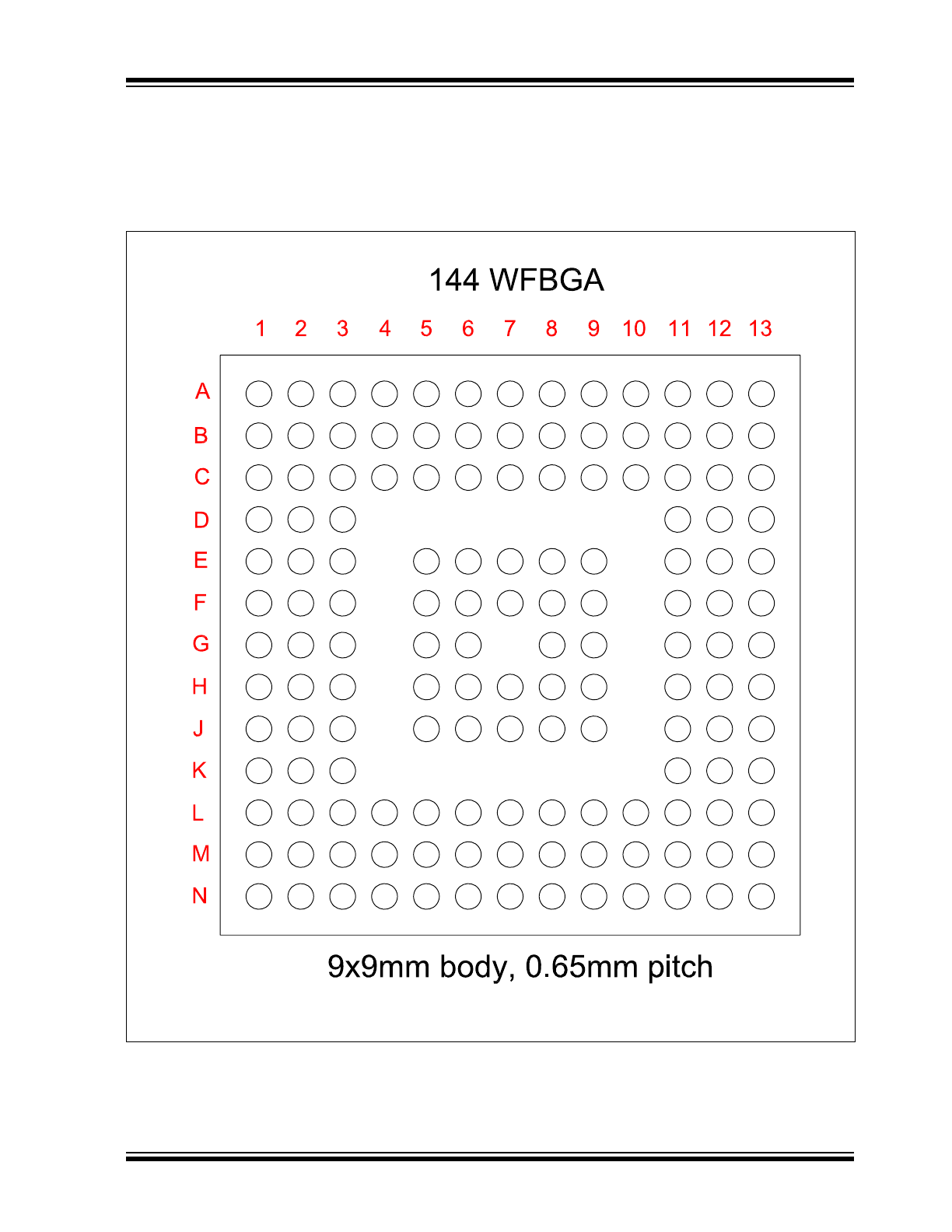
FIGURE 2-1:
SCH3227 PIN DIAGRAM

SCH3227/SCH3226/SCH3224/SCH3222
DS00002121B-page 8
2016-2017 Microchip Technology Inc.
Highlighted rows indicate balls whose function depends on the STRAPOPT strap input.
TABLE 2-1:
SCH3227 SUMMARIES BY STRAP OPTION
Ball#
Function: StrapOPT=1
Function: StrapOPT=0
K13
STRAPOPT (=VTR
a
)
STRAPOPT (=VSS
a
)
M4
RESERVED=VTR
b
RESERVED=VTR
b
C3
+12V_IN
+12V_IN
D3
+5V_IN
+5V_IN
E6
GP40
GP40
E3
VTR
VTR
E5
RESERVED=VSS
c
RESERVED=VSS
c
F8
TEST=VSS
c
TEST=VSS
c
F7
RESERVED=VSS
c
RESERVED=VSS
c
F3
VSS
VSS
F6
RESERVED=VSS
c
RESERVED=VSS
c
F5
RESERVED=VSS
c
RESERVED=VSS
c
G8
RESERVED=VSS
c
RESERVED=VSS
c
G6
RESERVED=VSS
c
RESERVED=VSS
c
H8
RESERVED=VSS
c
RESERVED=VSS
c
G5
RESERVED=VSS
c
RESERVED=VSS
c
H7
RESERVED=VSS
c
RESERVED=VSS
c
H6
RESERVED=VSS
c
RESERVED=VSS
c
H5
RESERVED=VSS
c
RESERVED=VSS
c
D2
CLOCKI
CLOCKI
E2
LAD0
LAD0
D1
LAD1
LAD1
E1
LAD2
LAD2
F2
LAD3
LAD3
F1
LFRAME#
LFRAME#
G2
LDRQ#
LDRQ#
H1
PCI_RESET#
PCI_RESET#
G1
PCI_CLK
PCI_CLK
H2
SER_IRQ
SER_IRQ
H3
VSS
VSS
J3
VCC
VCC
J1
GP44 / TXD6
nIDE_RSTDRV / GP44
J2
GP45 / RXD6
nPCIRST1 / GP45
K3
GP46 / nSCIN6
nPCIRST2 / GP46
L3
GP47 / nSCOUT6
nPCIRST3 / GP47
K1
AVSS
AVSS
L1
VBAT
VBAT
K2
GP27 / nIO_SMI / P17
GP27 / nIO_SMI / P17
L2
KDAT / GP21
KDAT / GP21
M1
KCLK / GP22
KCLK / GP22
M2
MDAT / GP32
MDAT / GP32
N1
MCLK / GP33
MCLK / GP33
M3
GP36 / nKBDRST
GP36 / nKBDRST

2016-2017 Microchip Technology Inc.
DS00002121B-page 9
SCH3227/SCH3226/SCH3224/SCH3222
N2
GP37 / A20M
GP37 / A20M
L5
VSS
VSS
N3
VTR VTR
N4
nINIT
nINIT
M5
nSLCTIN
nSLCTIN
L6
PD0
PD0
N5
PD1
PD1
M6
PD2
PD2
L7
PD3
PD3
N6
PD4
PD4
M7
PD5
PD5
N7
PD6
PD6
L8
PD7
PD7
L9
VSS
VSS
M8
SLCT
SLCT
N8
PE
PE
N9
BUSY
BUSY
M9
nACK
nACK
N10
nERROR
nERROR
M10
nALF
nALF
N11
nSTROBE
nSTROBE
M11
nRI1
nRI1
N12
nDCD1
nDCD1
L11
RXD1
RXD1
M12
TXD1 / SIOXNOROUT
TXD1 / SIOXNOROUT
N13
nDSR1
nDSR1
L12
nRTS1 / SYSOPT0
nRTS1 / SYSOPT0
M13
nCTS1
nCTS1
J12
nDTR1 / SYSOPT1
nDTR1 / SYSOPT1
K12
GP50 / nRI2
GP50 / nRI2
L13
VTR
VTR
J13
VSS
VSS
H11
GP51 / nDCD2
GP51 / nDCD2
H12
GP52 / RXD2(IRRX2)
GP52 / RXD2(IRRX2)
H13
GP53 / TXD2(IRTX2)
GP53 / TXD2(IRTX2)
G13
GP54 / nDSR2
GP54 / nDSR2
G12
GP55 / nRTS2 / RESGEN
GP55 / nRTS2 / RESGEN
G11
GP56 / nCTS2
GP56 / nCTS2
F13
GP57 / nDTR2
GP57 / nDTR2
F12
RXD5
PB_OUT#
F11
TXD5
PS_ON#
E13
nSCOUT5
PB_IN#
E12
nSCIN5
SLP_SX#
D13
GP10 / RXD3
GP10 / RXD3
TABLE 2-1:
SCH3227 SUMMARIES BY STRAP OPTION (CONTINUED)
Ball#
Function: StrapOPT=1
Function: StrapOPT=0

SCH3227/SCH3226/SCH3224/SCH3222
DS00002121B-page 10
2016-2017 Microchip Technology Inc.
D12
GP11 / TXD3
GP11 / TXD3
E11
GP14 / nDSR3
GP14 / nDSR3
C13
GP17 / nRTS3
GP17 / nRTS3
B13
GP16 / nCTS3
GP16 / nCTS3
C12
GP42 / nIO_PME
GP42 / nIO_PME
D11
VTR
VTR
A13
GP15 / nDTR3
GP15 / nDTR3
B12
GP61 / nLED2 / CLKO
GP61 / nLED2 / CLKO
C11
GP60 / nLED1 / WDT
GP60 / nLED1 / WDT
A12
GP13 / nRI3
GP13 / nRI3
B11
GP12 / nDCD3
GP12 / nDCD3
A11
GP31 / nRI4
GP31 / nRI4
C10
GP63 / nDCD4
GP63 / nDCD4
B10
CLKI32
CLKI32
A10
nRSMRST
nRSMRST
B9
VSS
VSS
C9
GP64 / RXD4
GP64 / RXD4
A9
GP65 / TXD4
GP65 / TXD4
A8
GP66 / nDSR4
GP66 / nDSR4
B8
GP67 / nRTS4
GP67 / nRTS4
C8
GP62 / nCTS4
GP62 / nCTS4
A7
GP34 / nDTR4
GP34 / nDTR4
B7
PWRGD_OUT
PWRGD_OUT
A6
PWRGD_PS
PWRGD_PS
C7
nFPRST / GP30
nFPRST / GP30
E8
VTR
VTR
E7
VSS
VSS
B6
nTHERMTRIP
nTHERMTRIP
A5
nHWM_INT
nHWM_INT
C6
PWM3
PWM3
B5
PWM2
PWM2
A4
PWM1
PWM1
B4
FANTACH3
FANTACH3
C5
FANTACH2
FANTACH2
C4
FANTACH1
FANTACH1
A3
HVSS
HVSS
B3
HVTR
HVTR
A2
REMOTE2-
REMOTE2-
A1
REMOTE2+
REMOTE2+
B1
REMOTE1- REMOTE1-
C1
REMOTE1+
REMOTE1+
C2
VCCP_IN
VCCP_IN
TABLE 2-1:
SCH3227 SUMMARIES BY STRAP OPTION (CONTINUED)
Ball#
Function: StrapOPT=1
Function: StrapOPT=0