

2016 Microchip Technology Inc.
DS00002120A-page 1
Product Features
• General Features
- 3.3 Volt Operation (5 Volt Tolerant)
- PC99, PC2001 Compliant
- ACPI Compliant
- Serial IRQ Interface Compatible with Serial-
ized IRQ Support for PCI Systems
- Two Address Options for Power On Configu-
ration Port
- System Management Interrupt (SMI)
• Low Pin Count Bus (LPC) Interface
• 33 General Purpose I/O pins
• Programmable Wake-up Event (PME) Interface
- Serial Modem RI Inputs
- GPIOs
- Watchdog
• 4 Full Function Serial Ports
- High Speed NS16C550A Compatible UARTs
with Send/Receive 16-Byte FIFOs
- Supports 230k and 460k Baud
- Programmable Baud Rate Generator
- Modem Control Circuitry
- 480 Address and 15 IRQ Options
• Infrared Communications Controller
- IrDA v1.2 (4Mbps), HPSIR, ASKIR,
Consumer IR Support
- 2 IR Ports
- 96 Base I/O Address, 15 IRQ, and 4 DMA
Options
• Two LED Drivers with Blinking Options
• Watchdog Timer
• Temperature Ranges Available
- Industrial (+85°C to -40°C)
- Commercial (+70°C to 0°C)
• 64-Ball WFBGA RoHS Compliant Package
SCH3221
LPC I/O with Quad UARTs, GPIO and Wake

SCH3221
DS00002120A-page 2
2016 Microchip Technology Inc.
TO OUR VALUED CUSTOMERS
It is our intention to provide our valued customers with the best documentation possible to ensure successful use of your Microchip
products. To this end, we will continue to improve our publications to better suit your needs. Our publications will be refined and
enhanced as new volumes and updates are introduced.
If you have any questions or comments regarding this publication, please contact the Marketing Communications Department via
E-mail at
docerrors@microchip.com
. We welcome your feedback.
Most Current Data Sheet
To obtain the most up-to-date version of this data sheet, please register at our Worldwide Web site at:
http://www.microchip.com
You can determine the version of a data sheet by examining its literature number found on the bottom outside corner of any page.
The last character of the literature number is the version number, (e.g., DS30000000A is version A of document DS30000000).
Errata
An errata sheet, describing minor operational differences from the data sheet and recommended workarounds, may exist for cur-
rent devices. As device/documentation issues become known to us, we will publish an errata sheet. The errata will specify the
revision of silicon and revision of document to which it applies.
To determine if an errata sheet exists for a particular device, please check with one of the following:
• Microchip’s Worldwide Web site;
http://www.microchip.com
• Your local Microchip sales office (see last page)
When contacting a sales office, please specify which device, revision of silicon and data sheet (include -literature number) you are
using.
Customer Notification System
Register on our web site at
www.microchip.com
to receive the most current information on all of our products.

2016 Microchip Technology Inc.
DS00002120A-page 3
SCH3221
Table of Contents
1.0 Introduction ..................................................................................................................................................................................... 4
2.0 Pin Layout ....................................................................................................................................................................................... 7
3.0 Description of Pin Functions ......................................................................................................................................................... 10
4.0 3.3 Volt Operation / 5 Volt Tolerance ............................................................................................................................................ 15
5.0 Power Functionality ....................................................................................................................................................................... 16
6.0 Functional Description .................................................................................................................................................................. 19
7.0 Runtime Registers ........................................................................................................................................................................ 52
8.0 Configuration ................................................................................................................................................................................. 61
9.0 Operational Description .............................................................................................................................................................. 102
10.0 Timing Diagrams ....................................................................................................................................................................... 106
11.0 XNOR-Chain Test Mode ........................................................................................................................................................... 115
12.0 Package Outline ........................................................................................................................................................................ 117
Appendix A: Data Sheet Revision History ......................................................................................................................................... 118
The Microchip Web Site .................................................................................................................................................................... 119
Customer Change Notification Service ............................................................................................................................................. 119
Customer Support ............................................................................................................................................................................. 119
Product Identification System ........................................................................................................................................................... 120

SCH3221
DS00002120A-page 4
2016 Microchip Technology Inc.
1.0
INTRODUCTION
1.1
Description
The SCH3221 is a 3.3V (5V tolerant) PC99/PC2001 compliant I/O controller with an LPC interface. The SCH3221
includes 4 Full-Function Serial Ports, IrDA and Consumer IR capability, GPIOs, and extensive PME Wake support from
these features.
The SCH3221 is ACPI compatible and supports multiple low power-down modes.
I/O functionality includes four serial ports. The serial ports are fully functional NS16550 compatible UARTs that support
data rates up to 460 Kbps. They all have the full 8 pin interface.
The PME Wake logic includes the ability to wake from a watchdog timer, any of the UART Ring Indicator (RI) Inputs, or
GPIOs.
SMI Generation is also supported.
System related functionality, which offers flexibility to the system designer, includes General Purpose I/O control func-
tions, a Watchdog Timer, and control of two LED's.
CAUTION: This device contains circuits which must not be used because their pins are not brought out of the package,
and are pulled to known states internally. Any features, and especially SIO blocks that are not listed in this document,
must not be activated or accessed. Doing so may cause unpredictable behavior and/or excessive currents, and there-
fore may damage the device and/or the system.
As part of this, it is also necessary to pull the GP57/nDTR2 pin low, as a strap, to disable LPC Memory cycle handling.
See
Note 3-12 on page 13
.
2016 Microchip Technology Inc.
DS00002120A-page 5
SCH3221
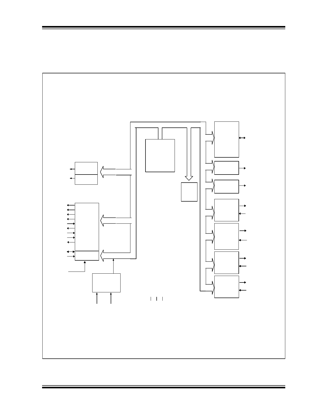
1.2
Block Diagram
FIGURE 1-1:
SCH3221 BLOCK DIAGRAM
SCH3221
Vcc Vss
V
TR
LPC BUS
INTERFACE
Serial
IRQ
SER_IRQ
PCI_CLK
LAD0
LAD1
LAD2
LAD3
LFRAME#
LDRQ#
LPCPD#
PCI_RESET#
CLKRUN#
CLOCK
GEN
CLOCKI
CLKI32
Denotes Multifunction Pins
*
16C550
COMPATIBLE
SERIAL
PORT 1
TXD1, nRTS1, nDTR1
nCTS1, RXD1,
nDSR1, nDCD1, nRI1
16C550
COMPATIBLE
SERIAL
PORT 4
TXD4*, nRTS4*, nDTR4*
nCTS4*, RXD*,
nDSR4*, nDCD*, nRI4*
16C550
COMPATIBLE
SERIAL
PORT 3
TXD3*, nRTS3,* nDTR3*
nCTS3*, RXD3*,
nDSR3*, nDCD3*, nRI3*
16C550
COMPATIBLE
SERIAL
PORT 2 WITH
INFRARED
INTERFACE
IRTX2*, IRMODE*,
TXD2*, nRTS2*, nDTR2*
IRRX2*, IRRX3*,
RXD2*, nCTS2*,
nDSR2*, nDCD2*, nRI2*
LED Driver
LED1*, LED2*
Watch Dog
Timer
WDT*
GP[11:13]*, GP[16:17]*,
GP[20:23]*,
GP[30:37]*,
GP[40:47]*,
GP[50:57]*
GENERAL
PURPOSE
I/O
CONTROL, ADDRESS, DATA
CONFIGURATION
REGISTERS
ACPI
BLOCK
nIO_PME
nIO_SMI*
S
M
I
P
M
E
IRQIN1*
IRQIN2*
IRQIN3*

SCH3221
DS00002120A-page 6
2016 Microchip Technology Inc.
1.3
References
1.
SMSC Infrared Communications Controller (IrCC) Specification, dated 5/10/96
2.
PCI Bus Power Management Interface Specification, Revision 1.0, Draft, March 18, 1997
3.
Low Pin Count (LPC) Interface Specification, Revision 1.0, September 29, 1997, Intel Document
4.
Advanced Configuration and Power interface Specification, Revision 1.0
2016 Microchip Technology Inc.
DS00002120A-page 7
SCH3221
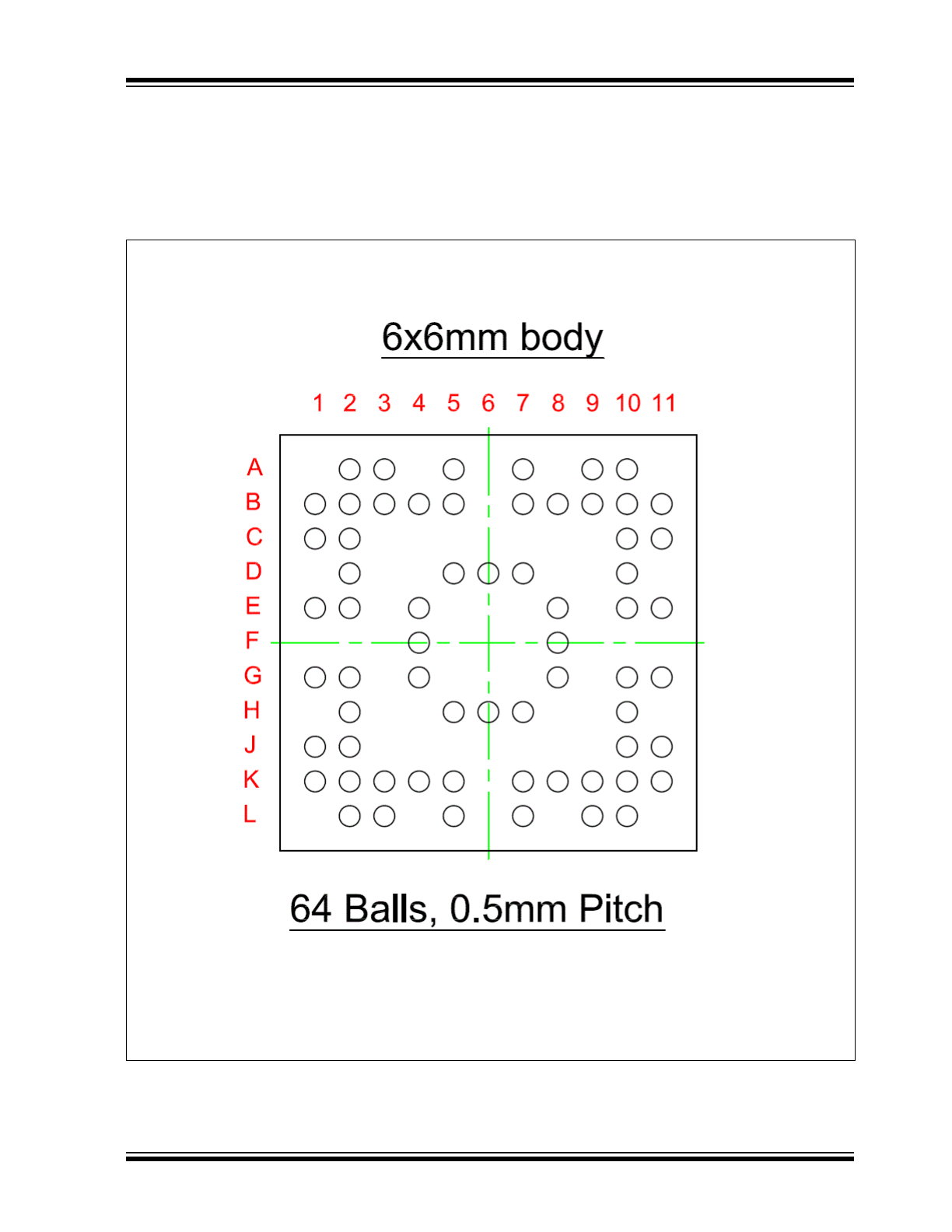
2.0
PIN LAYOUT
Figure 2-1
shows the ball footprint for the SCH3221. See
Table 2-1
below it for the pin function assignments.
FIGURE 2-1:
SCH3221 FOOTPRINT DIAGRAM, TOP VIEW

SCH3221
DS00002120A-page 8
2016 Microchip Technology Inc.
TABLE 2-1:
SCH3221 SUMMARY
BALL#
FUNCTION
B3
GP11
A3
TEST=VSS
B5
CLOCKI
D6
VSS
B2
CLKI32
B1
IO_PME#
F4
VTR
C1
GP23 / nLED2 / IRQIN2
E2
LAD0
D2
LAD1
E1
LAD2
G1
LAD3
E4
VCC
G2
LFRAME#
H5
VSS
B4
LDRQ#
A2
PCI_RESET#
J1
LPCPD#
J2
CLKRUN#
K1
PCI_CLK
K2
SER_IRQ
K3
GP30 / nRI3
L2
GP31 / nDCD3
L3
GP32 / RXD3
K4
GP33 / TXD3
H2
GP34 / nDSR3
L5
GP35 / nRTS3
K5
GP36 / nCTS3
L7
GP37 / nDTR3
G4
GP40 / nRI4
A5
GP41 / nDCD4
C2
GP42 / RXD4
L9
GP43 / TXD4
F8
GP44 / nDSR4
H6
GP45 / nRTS4
G8
GP46 / nCTS4
E8
VCC
K7
GP47 / nDTR4
J11
GP12 / IO_SMI#
H7
VSS
L10
GP13 / IRQIN1 / nLED1
K11
GP16
K8
GP17
K9
GP20 / IRRX2 / IRQIN3

2016 Microchip Technology Inc.
DS00002120A-page 9
SCH3221
J10
GP21 / IRTX2 / WDT
K10
GP22 / IRMODE / IRRX3
G11
RXD1
G10
TXD1
H10
nDSR1
A7
nRTS1 / SYSOPT
B7
nCTS1
E10
nDTR1
B8
nRI1
E11
nDCD1
C11
GP50 / nRI2
D10
GP51 / nDCD2
B9
GP52 / RXD2 / IRRX
C10
GP53 / TXD2 / IRTX
B10
GP54 / nDSR2
B11
GP55 / nRTS2
A10
GP56 / nCTS2
A9
GP57 / nDTR2
D5
VCC
D7
VSS
TABLE 2-1:
SCH3221 SUMMARY (CONTINUED)
BALL#
FUNCTION

SCH3221
DS00002120A-page 10
2016 Microchip Technology Inc.
3.0
DESCRIPTION OF PIN FUNCTIONS
The following section describes the functionality of the pins for the SCH3221.
TABLE 3-1:
PIN FUNCTIONS
Name
Function
Buffer Type
(
Note 3-1
)
Power Well
POWER PINS
VCC
+3.3 Volt Supply Voltage (
Note 3-8
)
VTR
+3.3 Volt Standby Supply Voltage (
Note 3-8
)
VSS
Ground
CLOCK PINS
CLKI32
32.768kHz Standby Clock Input (
Note 3-3
)
IS
VTR
CLOCKI
14.318MHz Clock Input
IS
VCC
SERIAL PORT 1 INTERFACE
RXD1
Receive Data 1
IS
VCC
TXD1
Transmit Data 1
O12
VCC
nDSR1
Data Set Ready 1
I
VCC
nRTS1
/SYSOPT
Request to Send 1 /(System Option) (
Note 3-4
)
OP14
VCC
nCTS1
Clear to Send 1
I
VCC
nDTR1
Data Terminal Ready 1
OP14
VCC
nRI1
Ring Indicator 1
I
VCC
(
Note 3-13
)
nDCD1
Data Carrier Detect 1
I
VCC
SERIAL PORT 2 INTERFACE
GP50 /nRI2
General Purpose I/O /Ring Indicator 2
IO8
VCC
(
Note 3-13
)
GP51 /nDCD2
General Purpose I/O /Data Carrier Detect 2
IO8
VCC
GP52
/RXD2
/IRRX
General Purpose I/O
/Receive Data 2
/IRRX
IS/O8
VCC
GP53
/TXD2
/IRTX
General Purpose I/O
/Transmit Data 2
/IRTX (
Note 3-6
,
Note 3-7
)
IO12
VCC
GP54
/nDSR2
General Purpose I/O
/Data Set Ready 2
IO8
VCC
GP55
/nRTS2
General Purpose I/O
/Request to Send 2
IO8
VCC
GP56 /nCTS2
General Purpose I/O /Clear to Send 2
IO8
VCC
GP57
/nDTR2
General Purpose I/O
/Data Terminal Ready 2
CAUTION: External pull-down is required on this
pin (
Note 3-12
).
IOP14
VCC
SERIAL PORT 3 INTERFACE
GP30
/nRI3
General Purpose I/O (
Note 3-11
)
/Ring Indicator 3
IO8
VCC
(
Note 3-13
)
GP31
/nDCD3
General Purpose I/O (
Note 3-11
)
/Data Carrier Detect 3
IO8
VCC
(
Note 3-13
)
GP32
/RXD3
General Purpose I/O (
Note 3-11
)
/Receive Data 3
IS/O8
VCC
(
Note 3-13
)