
2003 Microchip Technology Inc.
Preliminary
DS70090A-page 1
rfRXD0420/0920
Features:
• Low cost single conversion superheterodyne
receiver architecture
• Compatible with rfPIC™ and rfHCS series of RF
transmitters
• Easy interface to PICmicro
®
microcontroller
(MCU) and K
EE
L
OQ®
decoders
• VCO phase locked to quartz crystal reference:
- Narrow receiver bandwidth
- Maximizes range and interference immunity
• Selectable LNA gain control for improved dynamic
range
• Selectable IF bandwidth via external ceramic IF
filter
• Received Signal Strength Indicator (RSSI) for
signal strength indication (FSK, FM) and ASK
demodulation
• FSK/FM quadrature (phase coincidence) detector
demodulator
• 32-Lead LQFP package
UHF ASK/FSK Receiver:
• Single frequency receiver set by crystal frequency
• Receive frequency range:
• Maximum data rate:
- ASK: 80 Kbps NRZ
- FSK: 40 Kbps NRZ
• IF frequency range: 455 kHz to 21.4 MHz
• RSSI range: 70 dB
• Frequency deviation range: ±5 kHz to ±120 kHz
• Maximum FM modulation frequency: 15 kHz
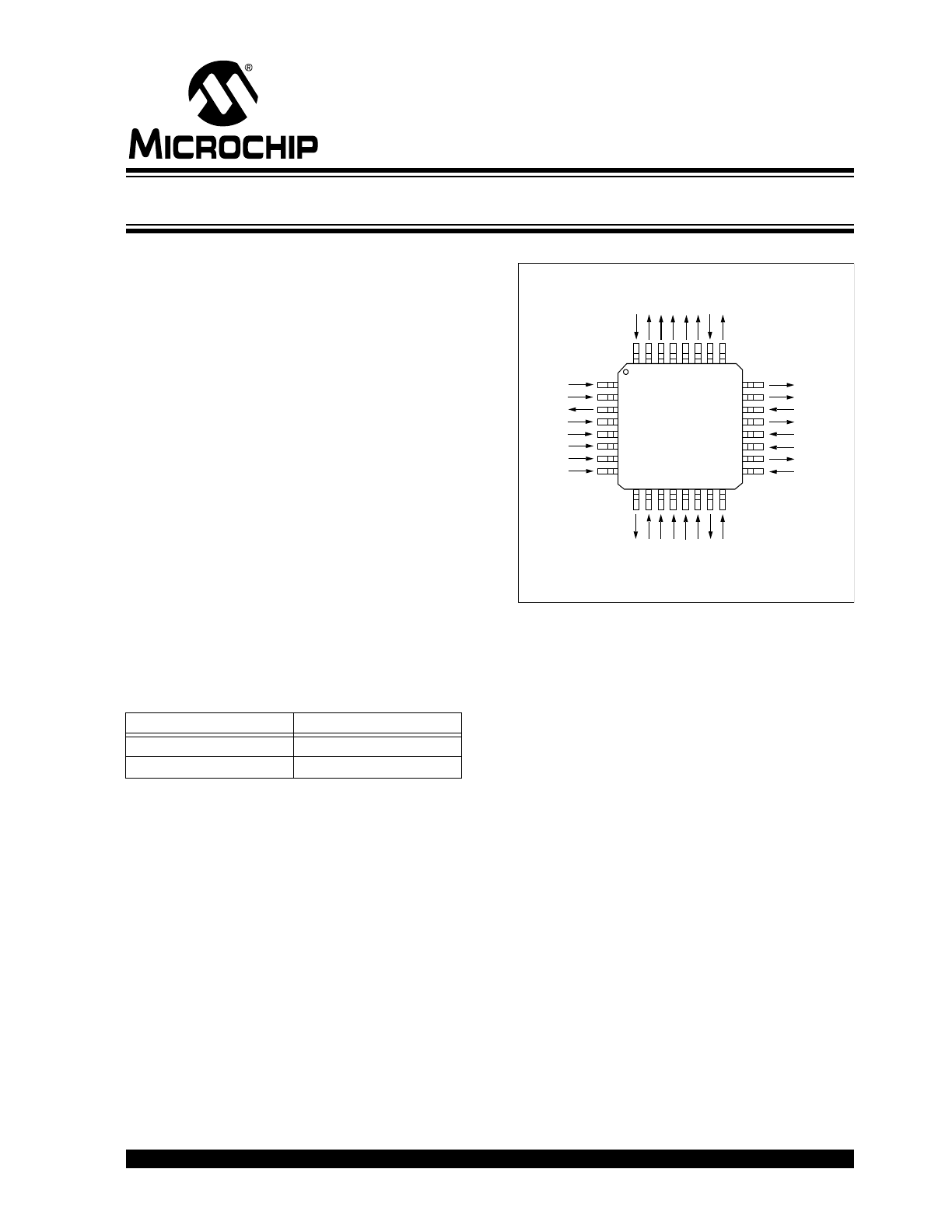
Pin Diagram:
Applications:
• Wireless remote command and control
• Wireless security systems
• Remote Keyless Entry (RKE)
• Low power telemetry
• Low power FM receiver
• Home automation
• Remote sensing
Bi-CMOS Technology:
• Wide operating voltage range
• Low current consumption in Active and Standby
modes
- rfRXD0420
- 8.2 mA (typical, LNA High Gain mode)
- <100 nA standby
- rfRXD0920
- 9.2 mA (typical, LNA High Gain mode)
- <100 nA standby
• Wide temperature range:
- Industrial: -40°C to +85°C
Device
Frequency Range
rfRXD0420
300 MHz to 450 MHz
rfRXD0920
800 MHz to 930 MHz
2
3
4
5
6
1
15 16
9 10 11 12
29
8
7
32 31 30
13 14
23
24
17
18
19
20
21
22
27
25
26
28
DEM
IN
2IF
OU
T
1IF
OUT
V
DD
FBC2
FBC1
2IF
IN
V
SS
V
DD
LNA
IN
V
SS
LF ENRX V
DD
XT
AL
V
SS
DEM
OUT
-
DEM
OUT
+
V
SS
RSSI
OPA+
OPA-
OPA
V
DD
V
SS
LNA
GAIN
LNA
OUT
1IF
IN
V
SS
1IF+
1IF-
V
DD
rfRXD0420
LQFP
rfRXD0920
UHF ASK/FSK/FM Receiver

rfRXD0420/0920
DS70090A-page 2
Preliminary
2003 Microchip Technology Inc.
1.0
DEVICE OVERVIEW
The rfRXD0420/0920 are low cost, compact single
frequency short-range radio receivers requiring only a
minimum number of external components for a
complete receiver system. The rfRXD0420 covers the
receive frequency range of 300 MHz to 450 MHz and
the rfRXD0920 covers 800 MHz to 930 MHz. The
rfRXD0420 and rfRXD0920 share a common architec-
ture. They can be configured for Amplitude Shift Keying
(ASK), Frequency Shift Keying (FSK), or FM modula-
tion. The rfRXD0420/0920 are compatible with rfPIC™
and rfHCS series of RF transmitters.
• High frequency stability over temperature and
power supply variations
• Low spurious signal emission
• High large-signal handling capability with
selectable LNA gain control for improved dynamic
range
• Selectable IF bandwidth via external low cost
ceramic IF filter. The IF Frequency range is
selectable between 455 kHz to 21.4 MHz. This
facilitates the use of readily available low cost
10.7 MHz ceramic IF filters in a variety of
bandwidths.
• ASK or FSK for digital data reception
• FM modulation for analog signal reception
• FSK/FM demodulation using quadrature detector
(phase coincidence detector)
• Received Signal Strength Indication (RSSI) for
signal strength indication and ASK detection
• Wide supply voltage range
• Low active current consumption
• Very low standby current
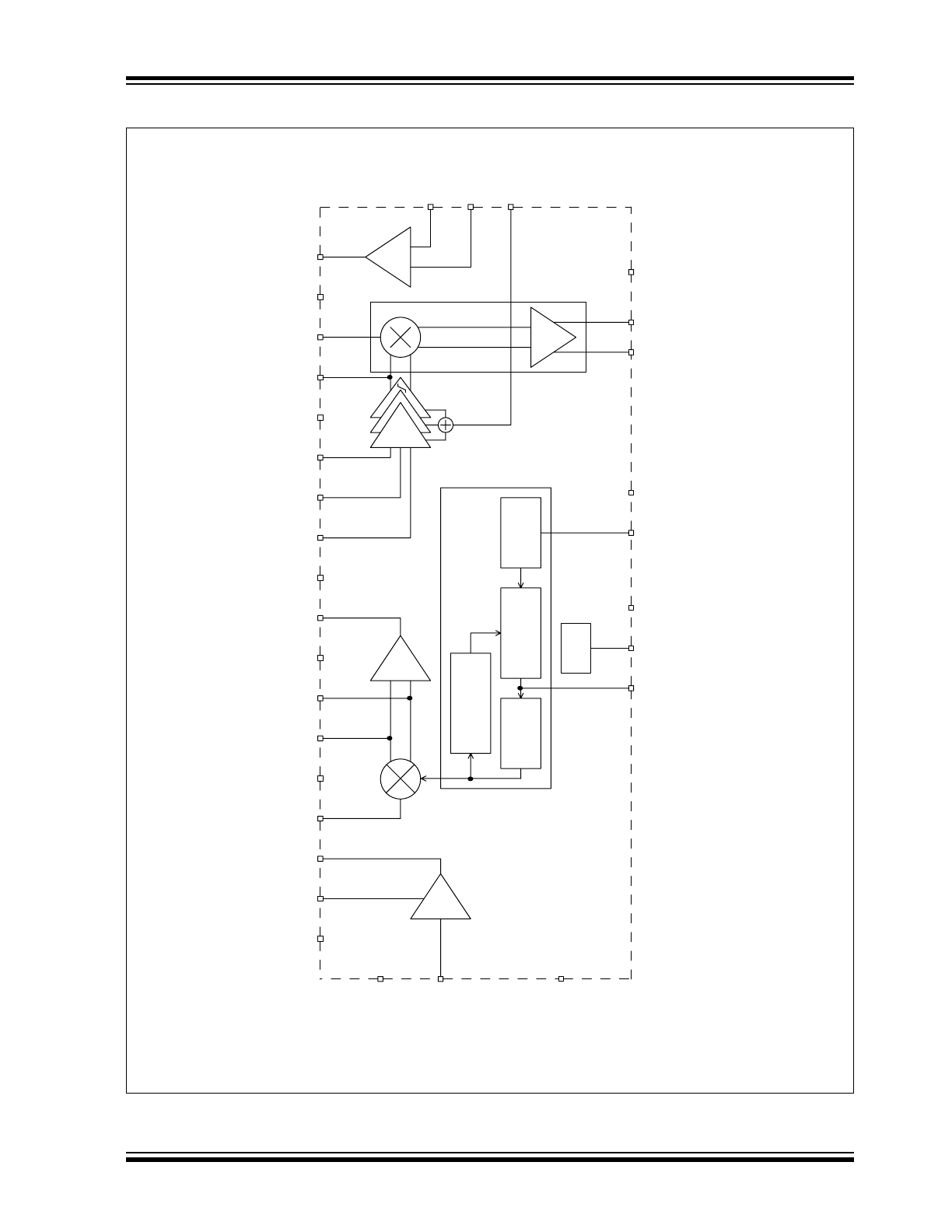
The rfRXD0420/0920 is a single conversion superhet-
erodyne architecture. A block diagram is illustrated in
Figure 1-1. The rfRXD0420/0920 consists of:
• Low-noise amplifier (LNA) - Gain selectable
• Mixer for down-conversion of the RF signal to the
Intermediate Frequency (IF) followed by an IF
preamplifier
• Fully integrated Phase-Locked Loop (PLL)
frequency synthesizer for generation of the Local
Oscillator (LO) signal. The frequency synthesizer
consists of:
- Crystal oscillator
- Phase-frequency detector and charge pump
- High-frequency Voltage Controlled Oscillator
(VCO)
- Fixed feedback divider
- rfRXD0420 = divide by 16
- rfRXD0920 = divide by 32
• IF limiting amplifier to amplify and limit the IF
signal and for Received Signal Strength Indication
(RSSI) generation
• Demodulator (DEMOD) section consists of a
phase detector (MIXER2) and amplifier creating a
quadrature detector (also known as a phase
coincidence detector) to demodulate the IF signal
in FSK and FM modulation applications
• Operational amplifier (OPA) that can be config-
ured as a comparator for ASK or FSK data
decision or as a filter for FM modulation.
• Bias circuitry for bandgap biasing and circuit
shutdown
2003 Microchip Technology Inc.
Preliminary
DS70090A-page 3
rfRXD0420/0920
FIGURE 1-1:
rfRXD0420/0920 BLOCK DIAGRAM
LNA
LNA
LNA
1IF
31
34
1IF+
1IF-
7
6
9
11
12
13
21
1IF
2IF
FBC1
FBC2
RSSI
20
19
18
OPA+
OPA-
OPA
XTAL
LF
29
26
Bias
ENRX
28
LNA
2
OPA
16
15
2IF
DEM
+
--
+-
OUT+
OUT-
24
23
DEMOD
IN
OUT
IN
OUT
IN
GAIN
OUT
IN
V
SS
1
V
SS
5
V
DD
8
V
SS
10
V
DD
14
V
DD
17
V
DD
32
V
SS
30
27
V
DD
25
V
SS
DEM
DEM
MIXER1
IF Preamp
IF Limiting Amplifier
MIXER2
22
V
SS
with RSSI
Crystal
Oscillator
Phase Detector
and
Charge Pump
Voltage
Controlled
Oscillator
Fixed Divide by
Frequency
Synthesizer
16: rfRXD0420
32: rfRXD0920
rfRXD0420/0920
DS70090A-page 4
Preliminary
2003 Microchip Technology Inc.
TABLE 1-1:
rfRXD0420/0920
PINOUT I/O DESCRIPTION
Pin Name
Pin Number
Pin Type
Buffer Type
Description
LNA
GAIN
2
I
CMOS
LNA gain control (with hysteresis)
LNA
OUT
3
O
Analog
LNA output (open collector)
1IF
IN
4
I
Analog
1st IF stage input
1IF+
6
--
Analog
MIXER1 bias (open collector)
1IF-
7
--
Analog
MIXER1 bias (open collector)
1IF
OUT
9
O
Analog
1st IF stage output
2IF
IN
11
I
Analog
2nd IF stage input
FBC1
12
--
Analog
Limiter IF Amplifier external feedback capacitor
FBC2
13
--
Analog
Limiter IF Amplifier external feedback capacitor
2IF
OUT
15
O
Analog
2nd IF stage output
DEM
IN
16
I
Analog
Demodulator input
OPA
18
O
Analog
Operational amplifier output
OPA-
19
I
Analog
Operational amplifier input (negative)
OPA+
20
I
Analog
Operational amplifier input (positive)
RSSI
21
O
Analog
Received signal strength indicator output
DEM
OUT
+
23
O
Analog
Demodulator output (positive)
DEM
OUT
-
24
O
Analog
Demodulator output (negative)
XTAL
26
I
Analog
Crystal oscillator input
ENRX
28
I
CMOS
Receiver enable input
LF
29
I
Analog
External loop filter connection. Common node of
charge pump output and VCO tuning input.
LNA
IN
31
I
Analog
LNA input
V
DD
8, 14, 17, 27, 32
P
Positive supply
V
SS
1, 5, 10, 25, 30
P
Ground reference
Legend: I = Input, O = Output, I/O = Input/Output, P = Power, CMOS = CMOS compatible input or output
2003 Microchip Technology Inc.
Preliminary
DS70090A-page 5
rfRXD0420/0920
2.0
CIRCUIT DESCRIPTION
This section gives a circuit description of the internal
circuitry of the rfRXD0420/0920 receiver. External
connections and components are given in the
APPLICATION CIRCUITS section.
2.1
Bias Circuitry
Bias circuitry provides bandgap biasing and circuit
shutdown capabilities. The ENRX (Pin 28) modes are
summarized in Table 2-1. The ENRX pin is a CMOS
compatible input and is internally pulled down to Vss.
2.2
Frequency Synthesizer
The Phase-locked Loop (PLL) frequency synthesizer
generates the Local Oscillator (LO) signal. It consists
of:
• Crystal oscillator
• Phase-frequency detector and charge pump
• Voltage Controlled Oscillator (VCO)
• Fixed feedback divider:
- rfRXD0420 = divide by 16
- rfRXD0920 = divide by 32
2.2.1
CRYSTAL OSCILLATOR
The internal crystal oscillator is a Colpitts type oscilla-
tor. It provides the reference frequency to the PLL. A
crystal is normally connected to the XTAL (Pin 26) and
ground. The internal capacitance of the crystal oscilla-
tor is 15 pF. Alternatively, a signal can be injected into
the XTAL pin from a signal source. The signal should
be AC coupled via a series capacitor at a level of
approximately 600 mV
pp
.
The XTAL pin is illustrated in Figure 2-1.
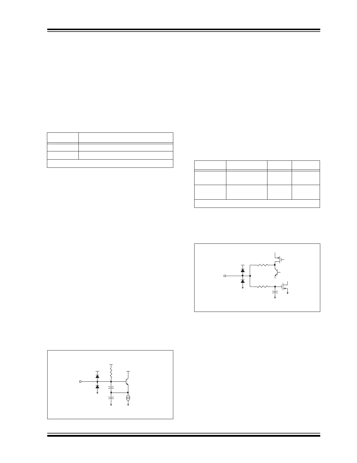
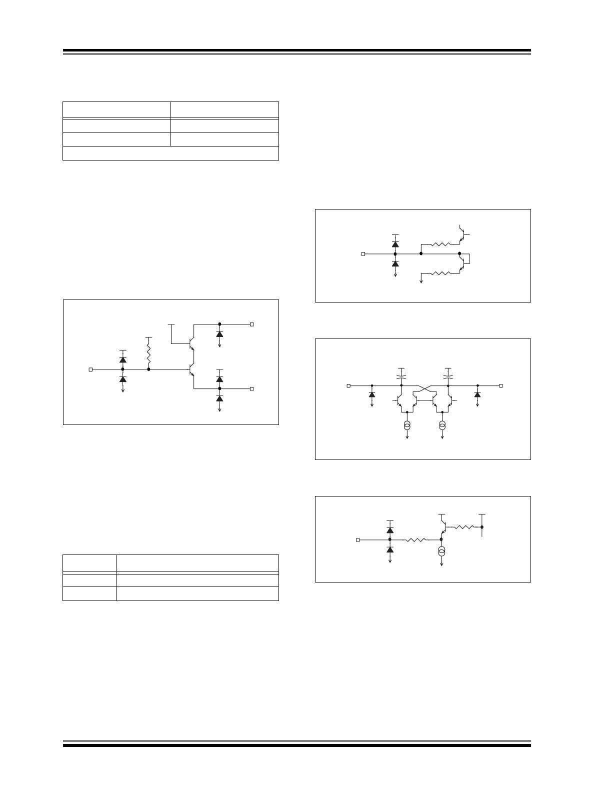
FIGURE 2-1:
BLOCK DIAGRAM OF
XTAL PIN
The PLL consists of a phase-frequency detector,
charge pump, voltage-controlled oscillator (VCO), and
fixed divide-by-16 (rfRXD0420) or divide-by-32
(rfRXD0920) divider. The rfRXD0420/0920 employs a
charge pump PLL that offers many advantages over
the classical voltage phase detector PLL: infinite pull-in
range and zero steady state phase error. The charge
pump PLL allows the use of passive loop filters that are
lower cost and minimize noise. Charge pump PLLs
have reduced flicker noise thus limiting phase noise.
An external loop filter is connected to pin LF (Pin 29).
The loop filter controls the dynamic behavior of the
PLL, primarily lock time and spur levels. The applica-
tion determines the loop filter requirements.
The VCO gain for the rfRXD0420/0920 receivers are
listed in Table 2-2.
The LF pin is illustrated in Figure 2-2.
FIGURE 2-2:
BLOCK DIAGRAM OF LOOP
FILTER PIN
2.3
Low Noise Amplifier
The Low-Noise Amplifier (LNA) is a high-gain amplifier
whose primary purpose is to lower the overall noise
figure of the entire receiver thus enhancing the receiver
sensitivity. The LNA is an open-collector cascode
design. The benefits of a cascode design are:
• high gain with low noise
• high-frequency
• wide bandwidth
• low effective input capacitance with stable input
impedance
• high output resistance
• high reverse isolation that provides improved
stability and reduces LO leakage
TABLE 2-1:
BIAS CIRCUITRY CONTROL
ENRX
(1)
Description
0
Standby mode
1
Receiver enabled
Note 1: ENRX has internal pull-down to Vss
XTAL
26
40 µA
V
SS
V
SS
V
SS
30 pF
30 pF
50 kΩ
V
DD
V
DD
V
DD
TABLE 2-2:
PLL PARAMETERS
Device
K
VCO(1)
I
CP(1)
Divider
rfRXD0420
250 MHz/V at
433 MHz
60
µA
16
rfRXD0920
300 MHz/V at
868 MHz
60
µA
32
Note 1: Typical value
LF
29
V
SS
V
SS
V
SS
4 pF
200 Ω
400 Ω
V
DD
rfRXD0420/0920
DS70090A-page 6
Preliminary
2003 Microchip Technology Inc.
Approximate LNA noise figures are listed in Table 2-3.
LNA
IN
(Pin 31) has an input impedance of approxi-
mately 26
Ω || 2 pF single-ended.
LNA
OUT
(Pin 3) has an open-collector output and is
pulled up to V
DD
via a tuned circuit.
Important: To ensure LNA stability the V
SS
pin (Pin 1)
must be connected to a low impedance ground.
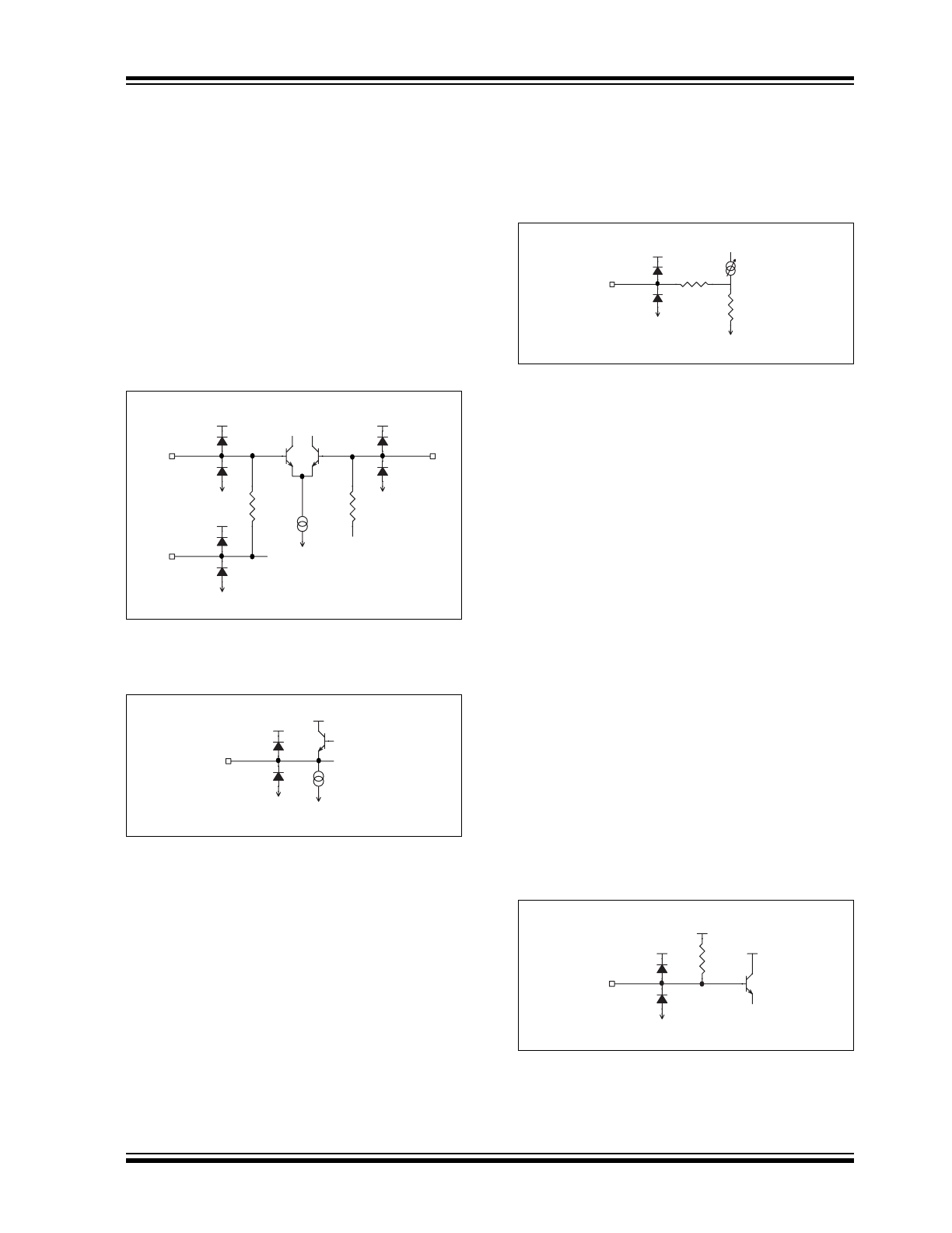
The LNA pins are illustrated in Figure 2-3.
FIGURE 2-3:
BLOCK DIAGRAM OF LNA
PINS
The gain of the LNA can be selected between High and
Low Gain modes by the LNA
GAIN
pin (Pin 2). LNA
GAIN
is a CMOS input with hysteresis. Table 2-4 summarizes
the voltage levels and modes for LNA gain.
In the High Gain mode the LNA operates normally. In
Low Gain mode the gain of the LNA is reduced approx-
imately 25 dB, reduces total supply current, and
increases maximum input signal levels (see Electrical
Characteristics section for values).
2.4
MIXER1 and IF Preamp
MIXER1 performs down-conversion of the RF signal to
the Intermediate Frequency (IF) and is followed by an
IF preamplifier.
1IF
IN
(Pin 4) has an approximately 33
Ω single-ended
input impedance. The 1IF
IN
pin is illustrated in Figure 2-
4.
The 1IF+ (Pin 6) and 1IF- (Pin 7) are bias connections
to the MIXER1 balanced collectors. Both pins are
open-collector outputs and are individually pulled up to
V
DD
by a load resistor. The MIXER1 bias pins are illus-
trated in Figure 2-5.
1IF
OUT
(Pin 9) has an approximately 330
Ω single-
ended output impedance. The 330
Ω impedance
provides a direct match to low cost ceramic IF filters.
The 1IF
OUT
pins is illustrated in Figure 2-6.
FIGURE 2-4:
BLOCK DIAGRAM OF MIXER1
PIN
FIGURE 2-5:
BLOCK DIAGRAM OF MIXER1
BIAS PINS
FIGURE 2-6:
BLOCK DIAGRAM OF IF
PREAMP PIN
2.5
IF Limiting Amplifier with RSSI
The IF Limiting Amplifier amplifies and limits the IF
signal at the 2IF
IN
pin (Pin 11). It also generates the
Received Signal Strength Indicator (RSSI) signal
(Pin 21).
2.5.1
IF LIMITING AMPLIFIER
Magnitude control circuitry is used in the last stage of
the receiver to keep the signal constant for demodula-
tion. It can consist of a limiting or Automatic Gain
Control (AGC) amplifier. A limiting amplifier is
TABLE 2-3:
LNA NOISE FIGURES
Device
Noise Figure
(1)
rfRXD0420
TBD
rfRXD0920
TBD
Note 1: Approximate value
TABLE 2-4:
LNA GAIN CONTROL
LNA
GAIN
Description
< 0.8 V
High Gain mode
> 1.4 V
Low Gain mode
LNA
LNA
31
3
IN
OUT
V
SS
1
V
SS
V
SS
V
SS
5 kΩ
V
DD
0.8V
1.6V
V
DD
1IF
4
IN
V
SS
V
SS
13 Ω
13 Ω
V
DD
500 µA
1IF+
6
500 µA
1IF-
7
500 µA
V
SS
V
SS
V
SS
V
SS
20 pF
20 pF
V
DD
V
DD
1IF
9
OUT
230 µA
V
SS
V
SS
130 Ω
6.8 kΩ
V
DD
V
DD
V
DD
2003 Microchip Technology Inc.
Preliminary
DS70090A-page 7
rfRXD0420/0920
employed in this design because it can handle a larger
dynamic range while consuming less power with simple
circuitry than AGC circuitry.
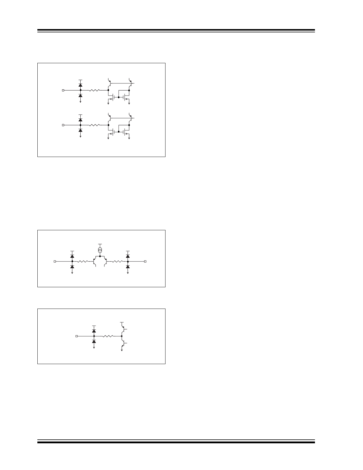
The internal resistance of the 2IF
IN
pin is approximately
2.2 k
Ω. In order to terminate ceramic IF filters whose
output impedance is 330
Ω, a 390 Ω resistor can be
paralleled to the 2IF
IN
and FBC2 pins.
FBC1 (Pin 12) and FBC2 (Pin 13) are connected to
external feedback capacitors.
The IF Limiting Amplifier pins are illustrated in
Figures 2-7 and 2-8.
FIGURE 2-7:
BLOCK DIAGRAM OF IF
LIMITING AMPLIFIER INPUT
PINS
FIGURE 2-8:
BLOCK DIAGRAM OF IF
LIMITING AMPLIFIER OUTPUT
PIN
2.5.2
RECEIVED SIGNAL STRENGTH
INDICATOR (RSSI)
The RSSI signal is proportional to the log of the signal
at 2IF
IN
. The 2IF
IN
input RSSI range is approximately
40
µV to 160 mV. The slope of the RSSI output is
approximately 26 mV/dB of RF signal.
The RSSI output has an internal 36 k
Ω resister to Vss
fed by a current source. This resistor converts the
RSSI current to voltage.
For Amplitude Shift Keying (ASK) demodulation, RSSI
is compared to a reference voltage (static or dynamic).
Post detector filtering is easily implemented by
connecting a capacitor to ground from the RSSI pin
effectively creating an RC filter with the internal 36 k
Ω
resistor.
For FSK and FM demodulation, the RSSI represents
the received signal strength of the incoming RF signal.
The RSSI pin is illustrated in Figure 2-9.
FIGURE 2-9:
BLOCK DIAGRAM OF RSSI
PIN
2.6
Demodulator
The demodulator (DEMOD) section consists of a phase
detector (MIXER2) and amplifier creating a quadrature
detector (also known as a phase coincidence detector)
to demodulate the IF signal in FSK and FM modulation
applications. The quadrature detector provides all the
IF functions required for FSK and FM demodulation
with only a few external parts.
The in-phase signal comes directly from the output of
the IF limiting amplifier to MIXER2. The quadrature
signal is created by an external tuned circuit from the
output of the IF limiting amplifier (2IF
OUT
, Pin 15) AC-
coupled to the MIXER2 DEM
IN
(Pin 16) input. The input
impedance of the DEM
IN
pin is approximately 47 k
Ω.
The external tuned circuit can be constructed from sim-
ple inductor-capacitor (LC) components but will require
one of the elements to be tunable. A no-tune solution
can be constructed with a ceramic discriminator.
The output voltage of the DEMOD amplifier (DEMout+
and DEMout-, Pins 23 and 24) depends on the peak
deviation of the FSK or FM signal and the Q of the
external tuned circuit. DEMout+ and DEMout- are high
impedance outputs with only a 20
µA current capability.
The Demodulator pins are illustrated in Figures 2-10
and 2-11.
FIGURE 2-10: BLOCK DIAGRAM OF
DEMODULATOR INPUT PIN
2IF
11
IN
200 µA
FBC2
13
FBC1
12
V
SS
Vss
V
SS
V
SS
2.2 kΩ
2.2 kΩ
V
DD
V
DD
V
DD
2IF
15
OUT
40 µA
V
SS
V
SS
V
DD
V
DD
RSSI
21
I (Pi)
V
SS
V
SS
50 Ω
36 kΩ
V
DD
DEM
16
IN
V
SS
47 kΩ
V
DD
V
DD
V
DD
rfRXD0420/0920
DS70090A-page 8
Preliminary
2003 Microchip Technology Inc.
FIGURE 2-11: BLOCK DIAGRAM OF
DEMODULATOR OUTPTUT
PINS
2.7
Operational Amplifier
The internal operational amplifier (OPA) can be
configured as a comparator for ASK or FSK or as a filter
for FM modulation applications.
The Op Amp pins are illustrated in Figures 2-12 and
2-13.
FIGURE 2-12: BLOCK DIAGRAM OF OP AMP
INPUT PINS
FIGURE 2-13: BLOCK DIAGRAM OF OP AMP
OUTPUT PIN
DEM
23
OUT+
DEM
24
OUT-
V
SS
V
SS
V
SS
V
SS
V
SS
V
SS
50 Ω
50 Ω
V
DD
20 µA
20 µA
V
DD
20 µA
20 µA
OPA-
19
OPA+
20
20 µA
V
SS
V
SS
50 Ω
50 Ω
V
DD
V
DD
V
DD
OPA
18
V
SS
V
SS
50 Ω
V
DD
V
DD
2003 Microchip Technology Inc.
Preliminary
DS70090A-page 9
rfRXD0420/0920
3.0
APPLICATION CIRCUITS
This section provides general information on applica-
tion circuits for the rfRXD0420/0920 receiver. The
following connections and external components
provide starting points for designs and list the minimum
circuitry recommended for general purpose
applications.
Performance of the radio system (transmitter and
receiver) is affected by component selection and the
environment in which it operates. Each system design
has its own unique requirements. Specifications for a
particular design requires careful analysis of the appli-
cation and compromises for a practical implementation.
3.1
General
This subsection lists connections and components that
are common between applications. The following
subsections give specific circuit connections and
components for ASK, FSK and FM applications.
3.1.1
BYPASS CAPACITORS
Bypass capacitors should be placed as physically close
as possible to V
DD
pins 8, 14, 17, 27 and 32
respectively. Additional bypassing and board level low-
pass filtering of the power supply may be required
depending on the application.
3.1.2
FREQUENCY PLANNING
The rfRXD0420/0920 receivers are single-conversion
superheterodyne architecture with a single IF
frequency. The receive frequency is set by the crystal
frequency (f
XTAL
) and intermediate frequency (f
if
). For
a majority of applications an external crystal is
connected to XTAL (Pin 26). Figure 3-1 illustrates an
example circuit with an optional trim capacitor.
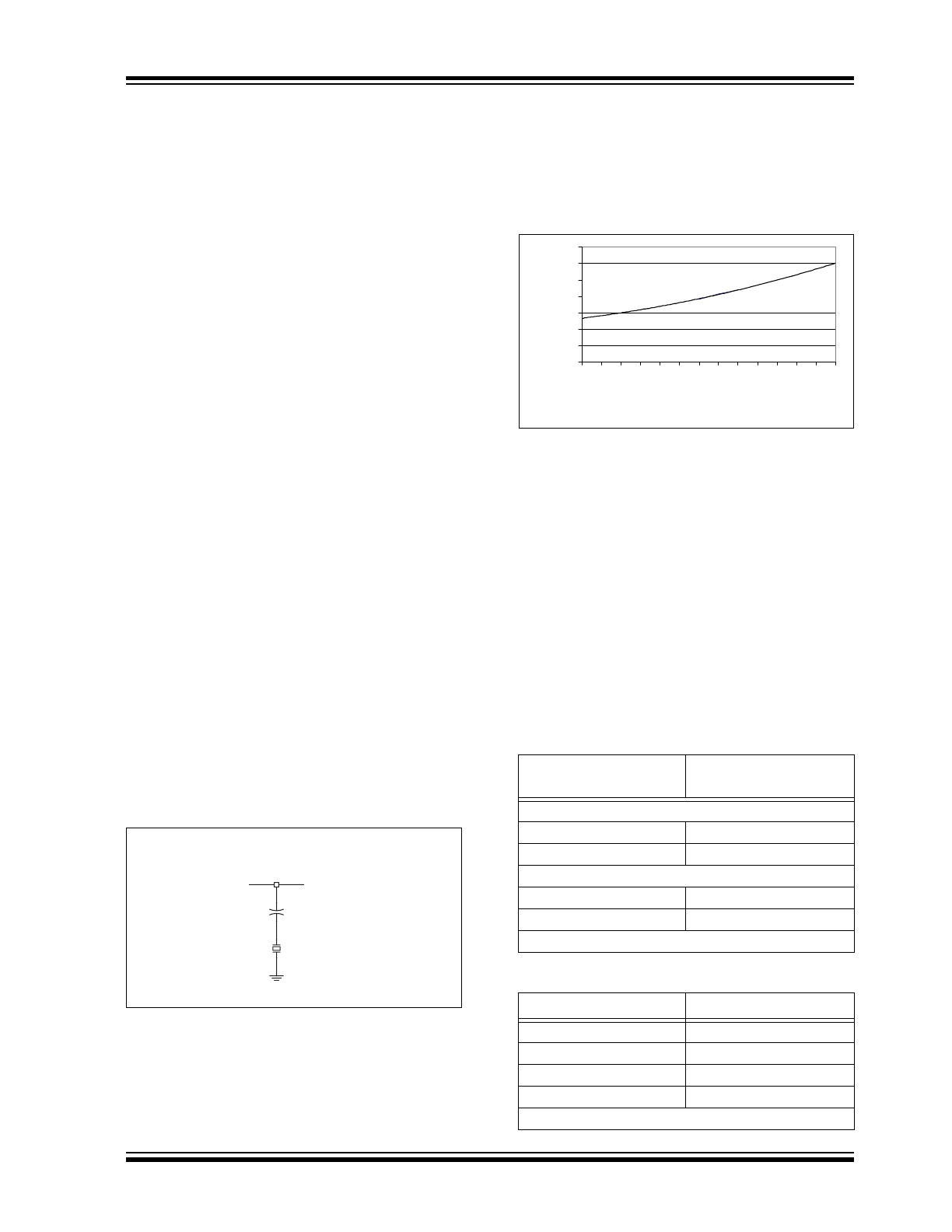
FIGURE 3-1:
XTAL EXAMPLE CIRCUIT
WITH OPTIONAL TRIM
CAPACITOR
The crystal load capacitance should be specified to
include the internal load capacitance of the XTAL pin of
15 pF plus PCB stray capacitance (approximately 2 to
3 pF). A trim capacitor can be used to trim the crystal
on frequency within the limitations of the crystal’s trim
sensitivity and pullability. Figure 3-2 illustrates the
effect the trim capacitor has on the receive frequency
for the rfRXD0420 at 433.92 MHz. Keep in mind that
this graph represents one example circuit and the
actual results depends on the crystal and PCB layout.
FIGURE 3-2:
RECEIVE FREQUENCY VS.
TRIM CAPACITANCE
Note that a 0
Ω resistor, in the lower left of the graph,
represents an infinite capacitance. This will be the
lowest frequency obtainable for the crystal and PCB
combination.
Calculation of the crystal frequency requires knowl-
edge of the receive frequency (f
rf
) and intermediate
frequency (f
if
). Figure 3-3 is a worksheet to assist the
designer in calculating the crystal frequency. Table 3-1
lists crystal frequencies for popular receive frequen-
cies. Table 3-2 lists crystal parameters required for
ordering crystals. For background information on
crystal selection see Application Note AN826, Crystal
Oscillator Basics and Crystal Selection for rfPIC
TM
and
PICmicro
®
Devices.
XTAL
26
C TRIM
(OPTIONAL)
X1
TABLE 3-1:
CRYSTAL FREQUENCIES FOR
POPULAR RECEIVE
FREQUENCIES
Receive
Frequency
Crystal
Frequency
rfRXD0420
315 MHz
20.35625 MHz
(2)
433.92 MHz
26.45125 MHz
(1)
rfRXD0920
868.3 MHz
26.8 MHz
(1)
915 MHz
28.259375 MHz
(1)
(1) Low-side injection (2) High-side injection
TABLE 3-2:
CRYSTAL PARAMETERS
Parameter
Value
Frequency:
(see Figure 3-1)
Mode:
Fundamental
Load Capacitance:
15-20 pF
ESR:
60
Ω Maximum
These values are for design guidance only.
433.75
433.80
433.85
433.90
433.95
434.00
434.05
434.10
0 ohms
82 pF
68 pF
56 pF
47 pF
39 pF
33 pF
27 pF
22 pF
18 pF
15 pF
12 pF
10 pF
5 pF
Trim Capacitor (pF)
Receive Frequency (MHz)
rfRXD0420/0920
DS70090A-page 10
Preliminary
2003 Microchip Technology Inc.
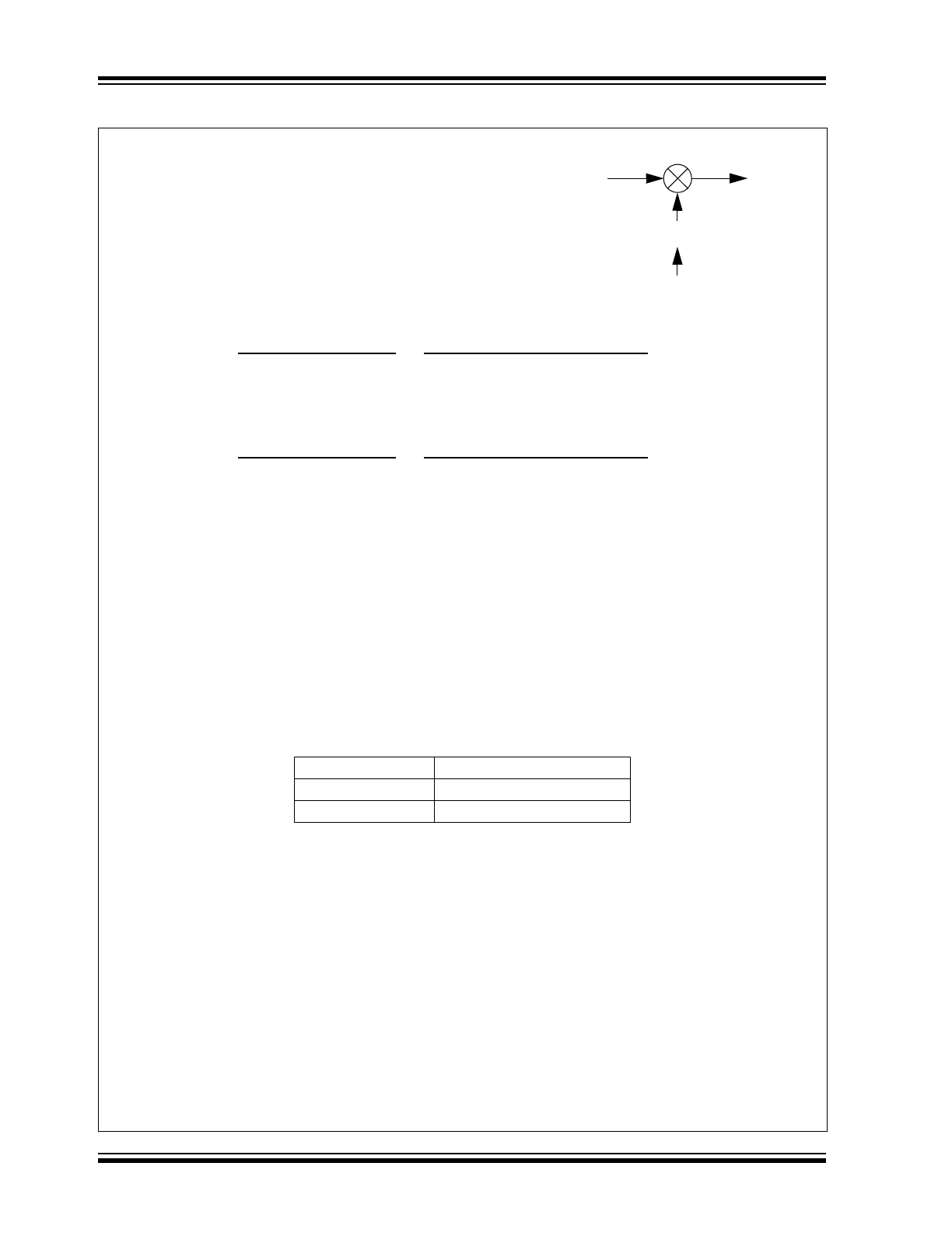
FIGURE 3-3:
FREQUENCY PLANNING WORKSHEET
Step 1: Identify receive (f
rf
) and IF frequency (f
if
).
Step 2: Calculate crystal frequencies for high- and low-side injection:
High-side Injection
Low-side Injection
Step 3: Calculate Local Oscillator (LO) frequencies (f
lo
) using f
XTAL-HIGH
and f
XTAL-LOW
:
High-side Injection
Low-side Injection
Step 4: Select high-side injection (f
lo-HIGH
) or low-side injection (f
lo-LOW
) that corresponds to the LO frequency
that is between the ranges of:
Step 5: From the chosen injection mode in Step 4, write the selected crystal frequency (f
XTAL
) and circle
injection mode.
Step 6: Calculate image frequency (f
rf-image
) for the Injection mode chosen:
if High-side Injection
if Low-side Injection
Note:
Image frequency should be sufficiently filtered by the preselector for the application.
f
rf
=
____________________
f
if
=
____________________
f
XTAL-HIGH
=
(
f
rf
+ f
if
)
=
(
_________ + _________
)
= _______________
PLL divide ratio
16 if rfRXD0420
32 if rfRXD0920
f
XTAL-LOW
=
(
f
rf
- f
if
)
=
(
_________ - _________
)
= _______________
PLL divide ratio
16 if rfRXD0420
32 if rfRXD0920
f
lo-HIGH
=
f
XTAL-HIGH
x PLL Divide Ratio =
_________ x
16 if rfRXD0420
= _____________
32 if rfRXD0920
f
lo-LOW
=
f
XTAL-LOW
x PLL Divide Ratio =
_________ x
16 if rfRXD0420
= _____________
32 if rfRXD0920
Device
LO Frequency Range
rfRXD0420
300 to 430 MHz
rfRXD0920
800 to 915 MHz
(circle one)
f
XTAL
=
____________________
High-side Injection
Low-side Injection
f
rf-image
=
f
rf
+ (2 x f
if
)
=
___________ + ( 2 x ___________ )
= ______________
f
rf-image
=
f
rf
- (2 x f
if
)
=
___________ - ( 2 x ___________ )
= ______________
f
rf
f
if
f
lo
f
XTAL
x PLL divide ratio