
© 2011 Microchip Technology Inc.
DS41189B-page 1
rfHCS362G/362F
General
• Combination K
EE
L
OQ®
encoder and synthesized
UHF ASK/FSK transmitter in a single package
• Operates on a single lithium coin cell
- <200 nA typical standby current
- 4.8 to 11.5 mA transmit current
- 2.2 to 5.5V operation
• Integrated solution with minimum external parts
• Separate pin-outs for K
EE
L
OQ
encoder and RF
transmitter provides for design flexibility
Code Hopping Encoder
• Programmable minimum code word completion
• Battery low signal transmitted to receiver with pro-
grammable threshold
• Non-volatile EEPROM storage of synchronization
data
• Easy to use EEPROM programming interface
• PWM or Manchester modulation
• Selectable encoder data rate 417 to 3334 bps
• On-chip tunable encoder oscillator
• RF Enable output for transmitter control
• Button inputs have internal pull-down resistors
• Elapsed time and button queuing options
• Current limiting on LED output
• 2-bit CRC for error detection
UHF ASK/FSK Transmitter
• Conforms to US FCC Part 15.231 regulations and
European ERC 70-03E and EN 300 220-1
requirements
• VCO phase locked to quartz crystal reference;
allows narrow receiver bandwidth to maximize
range and interference immunity
• Crystal frequency divide by 4 output (CLKOUT)
• Transmit frequency range (310 – 440 MHz) set by
Crystal frequency
• ASK Modulation
• FSK Modulation through crystal pulling
(rfHCS362F)
• Adjustable output power: -12 dBm to +2 dBm
• Differential output configurable for single or
double ended loop antenna
• Automatic power amplifier inhibit until PLL lock
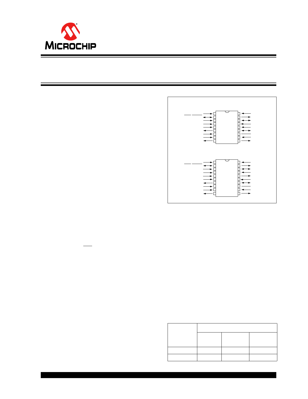
Pin Diagrams
Security
• Programmable 28/32-bit serial number
• Two programmable 64-bit encryption keys
• Programmable 60-bit seed
• Each 69-bit transmission is unique with 32 bits of
hopping code
• Encryption keys are read protected
Applications
• Automotive Remote Keyless Entry (RKE) systems
• Automotive alarm systems
• Automotive immobilizers
• Community gate and garage door openers
• Identity tokens with usage counters
• Burglar alarm systems
• Building access
Device
Features
Encrypt
Keys
Encoding
Transmitter
rfHCS362AG
2 x 64
PWM/MAN
ASK
rfHCS362AF
2 x 64
PWM/MAN
ASK/FSK
SOIC
V
SS
S2
XTAL
S3/RFEN
OUT
V
DD
LED/SHIFT
S1
RFEN
IN
CLKOUT
PS/DATA
ASK
V
DDRF
S0
LF
2
3
4
5
6
7
8
9
•1
17
16
14
13
12
11
10
15
18
r
fHCS36
2G
DATA
ANT2
NC
V
SSRF
ANT1
SSOP
V
SS
S2
DATA
FSK
S3/RFEN
OUT
V
DD
LED/SHIFT
S1
RFEN
IN
CLKOUT
PS/DATA
ASK
V
DDRF
S0
LF
2
3
4
5
6
7
8
9
•1
19
18
16
15
14
13
12
17
20
rf
HCS
36
2
F
DATA
NC
V
SSRF
ANT2
ANT1
10
11
FSK
OUT
XTAL
K
EE
L
OQ®
Code Hopping Encoder with
UHF ASK/FSK Transmitter

rfHCS362G/362F
DS41189B-page 2
© 2011 Microchip Technology Inc.
1.0
GENERAL DESCRIPTION
The rfHCS362G/362F is a code hopping encoder plus
UHF transmitter designed for secure wireless com-
mand and control systems. The rfHCS362G/362F uti-
lizes the K
EE
L
OQ
®
code hopping technology which
incorporates high security in a small package outline at
a low cost to make this device well suited for unidirec-
tional remote keyless entry systems and access control
systems.
The rfHCS362G/362F combines a 32-bit hopping code
generated by a nonlinear encryption algorithm with a
28/32-bit serial number and 9/5 status bits to create a
69-bit transmission stream. The length of the transmis-
sion strongly resists the threat of code scanning. The
code hopping mechanism makes each transmission
unique, thus rendering code capture and resend (code
grabbing) schemes virtually useless.
The encryption key, serial number and configuration
data are stored in an EEPROM array which is not
accessible via any external connection. The EEPROM
data is programmable but read protected. The data can
be verified only after an automatic erase and program-
ming operation. This protects against attempts to gain
access to keys or manipulate synchronization values.
The rfHCS362G/362F provides an easy to use serial
interface for programming the necessary keys, system
parameters and configuration data.
The transmitter is a fully integrated UHF ASK/FSK
transmitter consisting of crystal oscillator, Phase-
Locked Loop (PLL), open-collector differential-output
Power Amplifier (PA), and mode control logic. External
components consist of bypass capacitors, crystal, and
PLL loop filter. There are no internal electrical connec-
tions between the encoder and the transmitter. The
encoder oscillator is independent from the transmitter
crystal oscillator.
The rfHCS362G is capable of Amplitude Shift Keying
(ASK) modulation by turning the PA on and off. The
rfHCS362F is capable of ASK or Frequency Shift Key-
ing (FSK) modulation by employing an internal FSK
switch to pull the transmitter crystal via a second load
capacitor.
The rfHCS362G/362F is a single channel device. The
transmit frequency is fixed and set by an external refer-
ence crystal. Transmit frequencies in the range of 310
to 440 MHz can be selected. Output drive is an open-
collector differential amplifier. The differential output is
well suited for loop antennas. Output power is adjust-
able from +2 dBm to -12 dBm in six discrete steps.
The rfHCS362G/362F are radio frequency (RF) emit-
ting devices. Wireless RF devices are governed by a
country’s regulating agency. For example, in the United
States it is the Federal Communications Committee
(FCC) and in Europe it is the European Conference of
Postal and Telecommunications Administrations
(CEPT). It is the responsibility of the designer to ensure
that their end product conforms to rules and regulations
of the country of use and/or sale.
RF devices require correct board level implementation
in order to meet regulatory requirements. Layout con-
siderations are given in Section 6.0 UHF ASK/FSK
Transmitter.
1.1
Important Terms
The following is a list of key terms used throughout this
data sheet. For additional information on K
EE
L
OQ
and
Code Hopping refer to Technical Brief 3 (TB003).
• RKE - Remote Keyless Entry
• Button Status - Indicates what button input(s)
activated the transmission. Encompasses the 4
button status bits S3, S2, S1 and S0 (Figure 3-6).
• Code Hopping - A method by which a code,
viewed externally to the system, appears to
change unpredictably each time it is transmitted.
• Code word - A block of data that is repeatedly
transmitted upon button activation (Figure 3-6).
• Transmission - A data stream consisting of
repeating code words (Figure 10-1).
• Encryption key - A unique and secret 64-bit
number used to encrypt and decrypt data. In a
symmetrical block cipher such as the K
EE
L
OQ
algorithm, the encryption and decryption keys are
equal and will be referred to generally as the
encryption key.
• Encoder - A device that generates and encodes
data.
• Encryption Algorithm - A recipe whereby data is
scrambled using a encryption key. The data can
only be interpreted by the respective decryption
algorithm using the same encryption key.
• Decoder - A device that decodes data received
from an encoder.
• Decryption algorithm - A recipe whereby data
scrambled by an encryption algorithm can be
unscrambled using the same encryption key.
• Learn – Learning involves the receiver calculating
the transmitter’s appropriate encryption key,
decrypting the received hopping code and storing
the serial number, synchronization counter value
and encryption key in EEPROM. The K
EE
L
OQ
product family facilitates several learning strate-
gies to be implemented on the decoder. The fol-
lowing are examples of what can be done.
- Simple Learning
The receiver uses a fixed encryption key,
common to all components of all systems by
the same manufacturer, to decrypt the
received code word’s encrypted portion.
© 2011 Microchip Technology Inc.
DS41189B-page 3
rfHCS362G/362F
- Normal Learning
The receiver uses information transmitted
during normal operation to derive the encryp-
tion key and decrypt the received code
word’s encrypted portion.
- Secure Learn
The transmitter is activated through a special
button combination to transmit a stored 60-bit
seed value used to generate the transmitter’s
encryption key. The receiver uses this seed
value to derive the same encryption key and
decrypt the received code word’s encrypted
portion.
• Manufacturer’s code – A unique and secret 64-
bit number used to generate unique encoder
encryption keys. Each encoder is programmed
with a encryption key that is a function of the man-
ufacturer’s code. Each decoder is programmed
with the manufacturer code itself.
1.2
Applications
The rfHCS362G/362F is suited for secure wireless
remote control applications. The EEPROM technology
makes customizing application programs (transmitter
codes, appliance settings, etc.) extremely fast and con-
venient. The small footprint packages are suitable for
applications with space limitations. Low-cost, low-
power, high performance, ease of use and I/O flexibility
make the rfHCS362G/362F very versatile. Typical
application circuits are shown in Figure 1-5 and
Figure 1-6.
Most low-end keyless entry transmitters are given a
fixed identification code that is transmitted every time a
button is pushed. The number of unique identification
codes in a low-end system is usually a relatively small
number. These shortcomings provide an opportunity
for a sophisticated thief to create a device that ‘grabs’
a transmission and retransmits it later, or a device that
quickly ‘scans’ all possible identification codes until the
correct one is found.
The rfHCS362G/362F, on the other hand, employs the
K
EE
L
OQ
code hopping technology coupled with a trans-
mission length of 66 bits to virtually eliminate the use of
code ‘grabbing’ or code ‘scanning’. The high security
level of the rfHCS362G/362F is based on patented
technology. A block cipher based on a block length of
32 bits and a key length of 64 bits is used. The algo-
rithm obscures the information in such a way that even
if the transmission information (before coding) differs
by only one bit from that of the previous transmission,
the next coded transmission will be completely differ-
ent. Statistically, if only one bit in the 32-bit string of
information changes, approximately 50 percent of the
coded transmission bits will change.
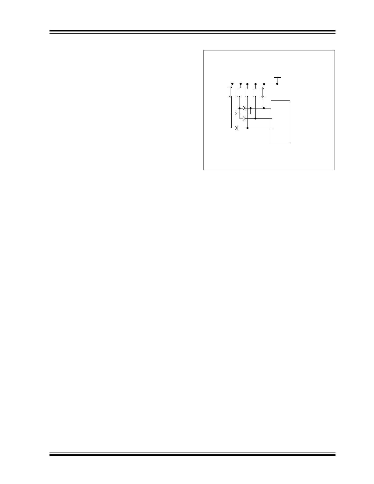
FIGURE 1-1: ADDITIONAL BUTTON INPUTS
Up to 7 button inputs can be implemented making them
look like a binary value to the 3 Sx inputs. This is done
with switching diodes as shown in Figure 1-1. The dis-
advantage is that simultaneously pressed buttons now
appear as if a single button is pressed.
The rfHCS362G/362F has a small EEPROM array
which must be loaded with several parameters before
use. These are most often programmed by the manu-
facturer at the time of production. The most important
of these are:
• A 28-bit serial number, typically unique for every
encoder
• An encryption key
• An initial 16-bit synchronization value
• A 16-bit configuration value
The encryption key generation typically inputs the
transmitter serial number and 64-bit manufacturer’s
code into the key generation algorithm (Figure 1-2).
The manufacturer’s code is chosen by the system
manufacturer and must be carefully controlled as it is a
pivotal part of the overall system security.
The 16-bit synchronization counter is the basis behind
the transmitted code word changing for each transmis-
sion; it increments each time a button is pressed. Due
to the code hopping algorithm’s complexity, each incre-
ment of the synchronization value results in about 50%
of the bits changing in the transmitted code word.
V
DD
S0
S1
S2
RFEN
B4 B3 B2 B1 B0
rfHCS362G/362F
DS41189B-page 4
© 2011 Microchip Technology Inc.
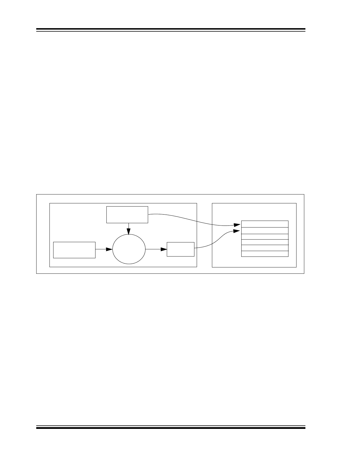
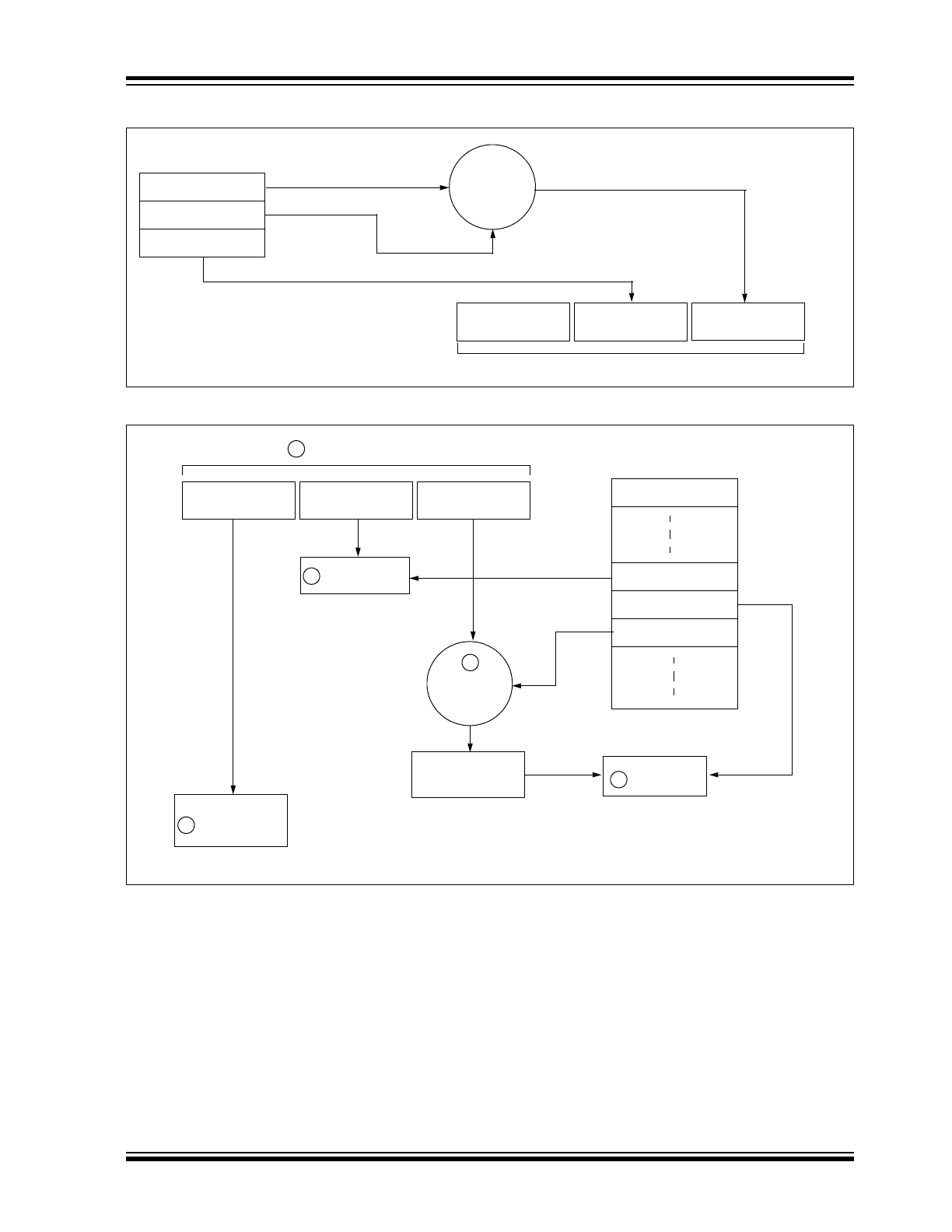
Figure 1-3 shows how the key values in EEPROM are
used in the encoder. Once the encoder detects a button
press, it reads the button inputs and updates the syn-
chronization counter. The synchronization counter and
encryption key are input to the encryption algorithm
and the output is 32 bits of encrypted information. This
data will change with every button press, its value
appearing externally to ‘randomly hop around’, hence it
is referred to as the hopping portion of the code word.
The 32-bit hopping code is combined with the button
information and serial number to form the code word
transmitted to the receiver. The code word format is
explained in greater detail in Section 3.1.
A receiver may use any type of controller as a decoder,
but it is typically a microcontroller with compatible firm-
ware that allows the decoder to operate in conjunction
with an rfHCS362G/362F based transmitter.
Section 7.0 provides detail on integrating the
rfHCS362G/362F into a system.
A transmitter must first be ‘learned’ by the receiver
before its use is allowed in the system. Learning
includes calculating the transmitter’s appropriate
encryption key, decrypting the received hopping code
and storing the serial number, synchronization counter
value and encryption key in EEPROM.
In normal operation, each received message of valid
format is evaluated. The serial number is used to deter-
mine if it is from a learned transmitter. If from a learned
transmitter, the message is decrypted and the synchro-
nization counter is verified. Finally, the button status is
checked to see what operation is requested. Figure 1-4
shows the relationship between some of the values
stored by the receiver and the values received from
the transmitter.
FIGURE 1-2:
CREATION AND STORAGE OF ENCRYPTION KEY DURING PRODUCTION
Transmitter
Manufacturer’s
Serial Number
Code
Encryption
Key
Key
Generation
Algorithm
Serial Number
Encryption Key
Sync Counter
.
.
.
rfHCS362
Production
Programmer
EEPROM Array
© 2011 Microchip Technology Inc.
DS41189B-page 5
rfHCS362G/362F
FIGURE 1-3:
BUILDING THE TRANSMITTED CODE WORD (ENCODER)
FIGURE 1-4:
BASIC OPERATION OF RECEIVER (DECODER)
NOTE: Circled numbers indicate the order of execution.
Button Press
Information
EEPROM Array
32 Bits
Encrypted Data
Serial Number
Transmitted Information
Encryption Key
Sync Counter
Serial Number
K
EE
L
OQ®
Encryption
Algorithm
Button Press
Information
EEPROM Array
Manufacturer Code
32 Bits of
Encrypted Data
Serial Number
Received Information
Decrypted
Synchronization
Counter
Check for
Match
Sync Counter
Serial Number
K
EE
L
OQ®
Decryption
Algorithm
1
3
4
Check for
Match
2
Perform Function
Indicated by
button press
5
Encryption Key
rfHCS362G/362F
DS41189B-page 6
© 2011 Microchip Technology Inc.
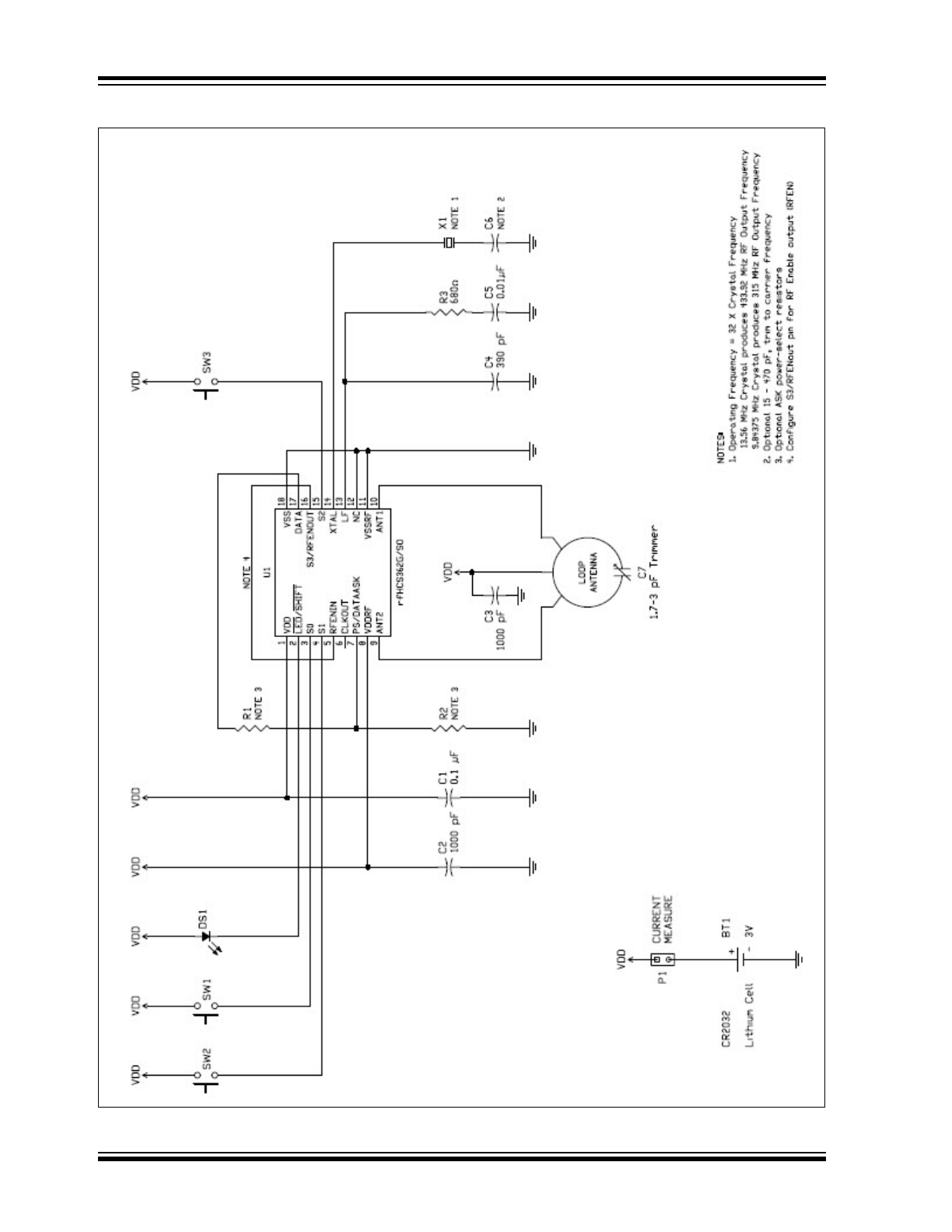
FIGURE 1-5:
ASK EXAMPLE APPLICATIONS CIRCUIT
© 2011 Microchip Technology Inc.
DS41189B-page 7
rfHCS362G/362F
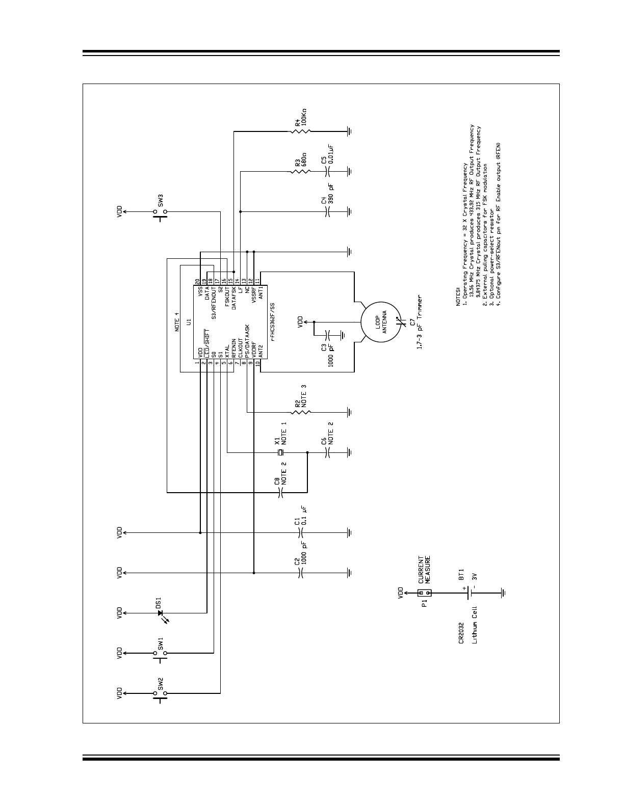
FIGURE 1-6:
FSK EXAMPLE APPLICATIONS CIRCUIT
rfHCS362G/362F
DS41189B-page 8
© 2011 Microchip Technology Inc.
2.0
DEVICE DESCRIPTION
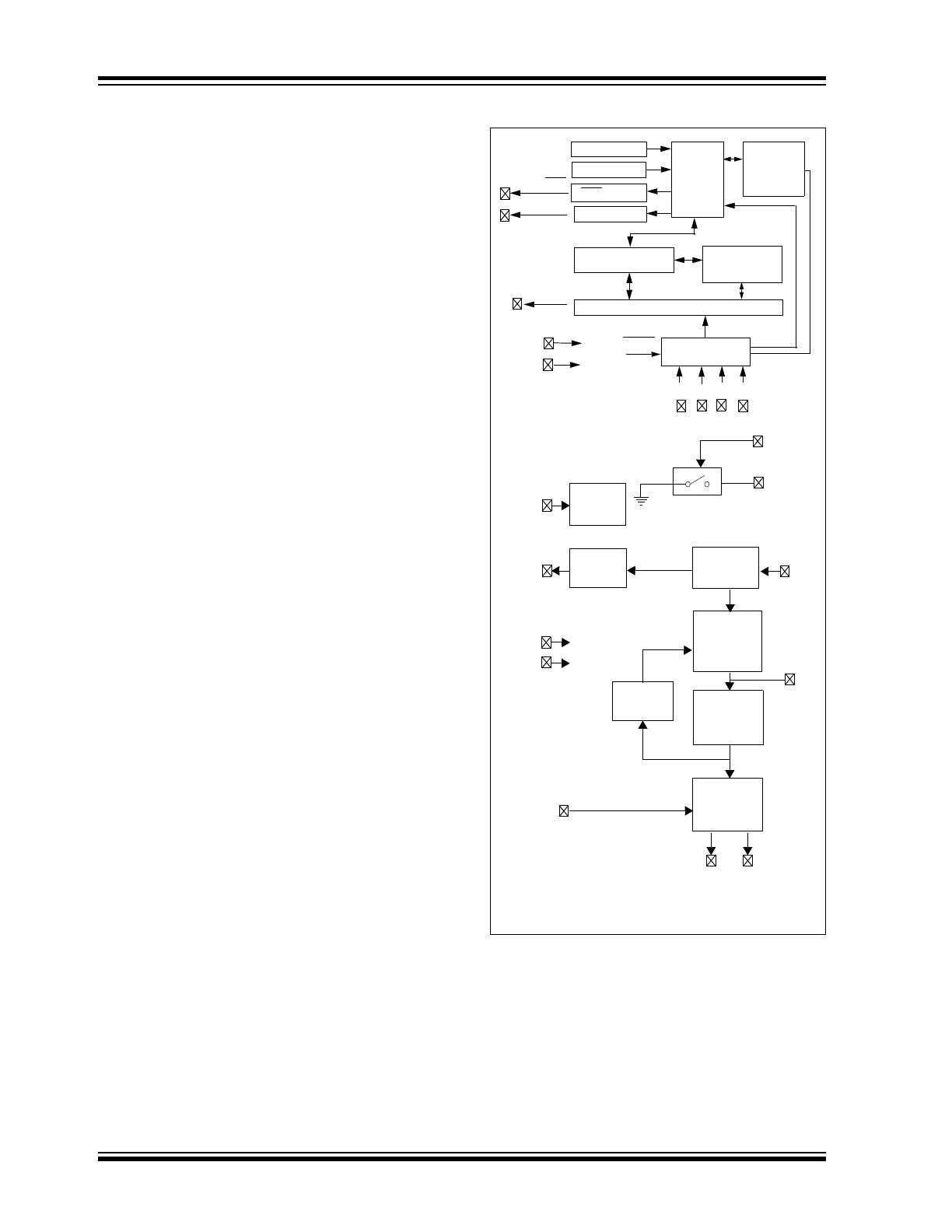
The block diagram in Figure 2-1 shows the internal
configuration with the top half representing the encoder
and the bottom half the UHF transmitter. Note that con-
nections between the encoder and transmitter are
made external to the device for more versability.
Typical application circuits are shown in Figure 1-5 and
Figure 1-6. The rfHCS362G/362F requires only the
addition of push button switches and few external com-
ponents for use as a transmitter in your security appli-
cation. See Table 2-1 for pinout description. Figure 2-2
shows the device I/O circuits.
FIGURE 2-1:
rfHCS362 BLOCK DIAGRAM
V
SS
V
DD
Oscillator
RESET Circuit
LED Driver
Controller
Power
Latching
and
Switching
Button Input Port
32-bit Shift Register
Encoder
EEPROM
DATA
LED
S3 S2 S1 S0
SHIFT
PLL Driver
RFEN
RFEN
IN
Divide
by 4
Mode
Control
Logic
CLKOUT
Power
Amplifier
(PA)
Crystal
Oscillator
ANT2
ANT1
XTAL
Phase
Detector
and
Charge Pump
Voltage
Controlled
Oscillator
(VCO)
Fixed
Divide
by 32
LF
PS/DATA
ASK
DATA
FSK (1)
FSK
OUT
(1)
FSK Switch
V
DDRF
V
SSRF
Note 1: rfHCS362F only.

© 2011 Microchip Technology Inc.
DS41189B-page 9
rfHCS362G/362F
TABLE 2-1:
rfHCS362G/362F PINOUT DESCRIPTION
Name
SOIC
Pin #
SSOP
Pin #
I/O/P
Type
Description
ANT1
10
11
O
Antenna connection to differential power amplifier output, open
collector.
ANT2
9
10
O
Antenna connection to differential power amplifier output, open
collector.
CLKOUT
6
7
O
Clock output.
DATA
17
19
I/O
Encoder data output pin or serial programming.
DATA
FSK
—
15
I
FSK data input.
FSK
OUT
—
16
O
FSK crystal pulling output.
LED/SHIFT
2
2
I/O
Current limited LED driver. Input sampled before LED driven.
LF
13
14
—
External loop filter connection. Common node of charge pump
output and VCO tuning input.
PS/DATA
ASK
7
8
I
Power select and ASK data input.
RFEN
IN
5
6
I
Transmitter and CLKOUT enable. Internal pull-down.
S0
3
3
I
Switch input 0 with internal pull-down.
S1
4
4
I
Switch input 1 with internal pull-down.
S2
15
17
I
Switch input 2 with internal pull-down or Schmitt Trigger clock
input during serial programming.
S3/RFEN
16
18
I/O
Switch input 3 with internal pull-down or RF enable output as
selected by RFEN option in configuration word SEED_3.
V
DD
1
1
P
Positive supply for encoder
V
DDRF
8
9
P
Positive supply for transmitter.
V
SS
18
20
P
Ground reference for encoder
V
SSRF
11
12
P
Ground reference for transmitter.
XTAL
14
5
I
Transmitter crystal connection to Colpitts type crystal oscillator.
Legend: I = input, O = output, I/O = input/output, P = power
rfHCS362G/362F
DS41189B-page 10
© 2011 Microchip Technology Inc.
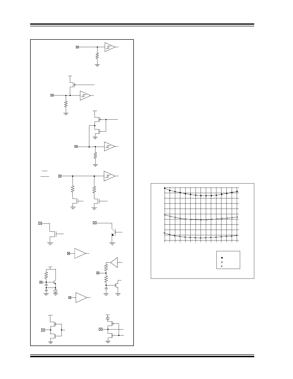
FIGURE 2-2:
I/O CIRCUITS
2.1
Encoder Architectural Overview
2.1.1
ONBOARD EEPROM
The rfHCS362G/362F has an onboard nonvolatile
EEPROM which is used to store user programmable
data. The data can be programmed at the time of pro-
duction and includes the security-related information
such as encoder keys, serial numbers, discrimination
and seed values. All the security related options
are read protected. The rfHCS362G/362F has built-in
protection against counter corruption. Before every
EEPROM write, the internal circuitry also ensures that
the high voltage required to write to the EEPROM is at
an acceptable level.
2.1.2
INTERNAL RC OSCILLATOR
The rfHCS362G/362F has an onboard RC oscillator
that controls all the logic output timing characteristics.
The oscillator frequency varies within ±10% of the
nominal value (once calibrated over a voltage range of
2V – 3.5V or 3.5V – 6.3V). All the timing values
specified in this document are subject to the oscillator
variation.
FIGURE 2-3:
TYPICAL rfHCS362G/362F
NORMALIZED OSCILLATOR
PERIOD VS. TEMPERATURE
S0, S1, S2,
RS
Inputs
V
DD
RFEN
S3 Input/
RS
RDATA
DATA I/O
LED output
RL
RH
V
DD
DATA
LEDH
LEDL
RFEN Output
PFET
NFET
PFET
NFET
NFET
SHIFT input
SHIFT
RFEN
IN
NFET
FSK
OUT
OUTPUT
ANT1, ANT2 outputs
CLKOUT
V
DDRF
PFET
NFET
PS/DATA
ASK
V
DDRF
V
P
LL
Lock
20
μA
V
DDRF
V
VCO
5 pF
200
Ω
200
Ω
Change
Pump
LF
RFEN
IN
input
XTAL
output
PS
DATA
FSK
input
0.94
1.10
1.08
1.06
1.04
1.02
1.00
0.98
0.96
0.92
0.90
V
DD
Legend
= 2.0V
= 3.0V
= 6.0V
Temperature °C
-50-40-30-20-10 0 10 20 30 40 50 6070 80 90
Note: Values are for calibrated oscillator