
© 2008 Microchip Technology Inc.
DS22114A-page 1
MCP9509/10
Features
• Resistor-Programmable Temperature Switch
• Wide Operating Voltage Range: 2.7V to 5.5V
• Low Supply Current: 30 µA (typical)
• Temperature Switch Accuracy:
- ±0.5°C (typical) at +25°C, +45°C
- ±1°C (typical) 0°C to +70°C
- ±3.5°C (maximum) 0°C to +125°C
- ±4.5°C (maximum) -20°C to +125°C
- ±2°C (typical) -40°C to +125°C
• Sensor Options available:
- Switch for rising temperature: Cold
to
Hot (H)
- Switch for falling temperature: Hot
to Cold (C)
• Output Configurations:
- Open-Drain:
– External Pull-up Resistor: MCP9509
– Internal Pull-up Resistor: MCP9510
- Active-Low, Push-Pull: MCP9510
- Active-High, Push-Pull: MCP9510
• User Selectable Hysteresis: 2°C or 10°C (typical)
• Space-Saving SOT-23-5, SOT-23-6 Packages
Applications
• Power Supply Thermal Shutdown
• Temperature Alarm
• Thermostat Control
• Fan Control
• Base-Stations
• Automotive
Typical Performance
Description
Microchip Technology’s MCP9509/10 devices are pro-
grammable logic output temperature switches. The
temperature switch threshold can be programmed with
a single external resistor, which provides high design
flexibility and simplicity. In addition, this family of
devices provide user programmable features such as
2°C and 10°C (typical) switch hysteresis and output
structure configuration. The MCP9509 provides an
open drain output, whereas the MCP9510 is offered in
three different user selectable output configurations:
Active-low/Active-high push pull and Active-Low
Open-Drain output with an internal 100 k
Ω pull-up
resistor.
The MCP9509/10 operate from 2.7V to 5.5V. This
family is capable of triggering for temperatures -40°C to
+125°C with high accuracy.
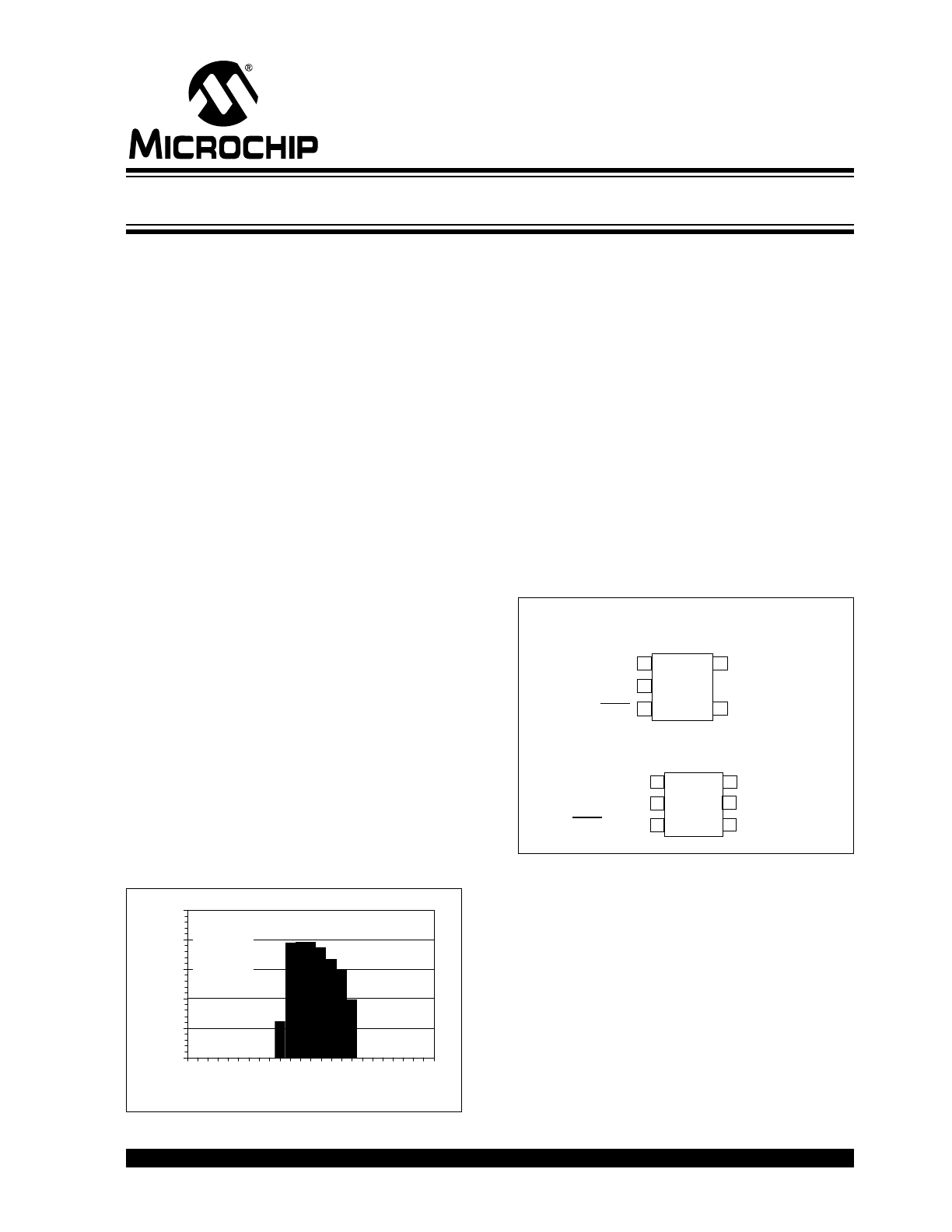
Package Types
0%
4%
8%
12%
16%
20%
-3
.0
-2
.0
-1
.0
0.
0
1.
0
2.
0
3.
0
Temperature Accuracy (°C)
O
c
c
u
rr
en
ce
s
T
A
= +45°C
V
DD
= 4.1V
9087 Units
6 Lots
4
1
2
3
5
GND
OUT
SOT-23-5
MCP9509
SET
V
DD
HYST
4
1
2
3
6
GND
OUT / OUT
SOT-23-6
MCP9510
SET
V
DD
HYST
5 OUTSET
Resistor-Programmable Temperature Switches

MCP9509/10
DS22114A-page 2
© 2008 Microchip Technology Inc.
NOTES:
© 2008 Microchip Technology Inc.
DS22114A-page 3
MCP9509/10
1.0
ELECTRICAL
CHARACTERISTICS
Absolute Maximum Ratings †
V
DD
.................................................................................. 6.0V
Voltage at all Input/Output pins ............... GND – 0.3V to 6.0V
Input/Output Current .....................................................20 mA
Storage temperature .....................................-65°C to +150°C
Ambient temp. with power applied ................-40°C to +125°C
Junction Temperature (T
J
) .......................................... +150°C
ESD protection on all pins (HBM:MM) ................. (4 kV/400V)
Latch-Up Current at each pin (25°C) ....................... ±200 mA
†Notice: Stresses above those listed under “Maximum
ratings” may cause permanent damage to the device. This is
a stress rating only and functional operation of the device at
those or any other conditions above those indicated in the
operational listings of this specification is not implied.
Exposure to maximum rating conditions for extended periods
may affect device reliability.
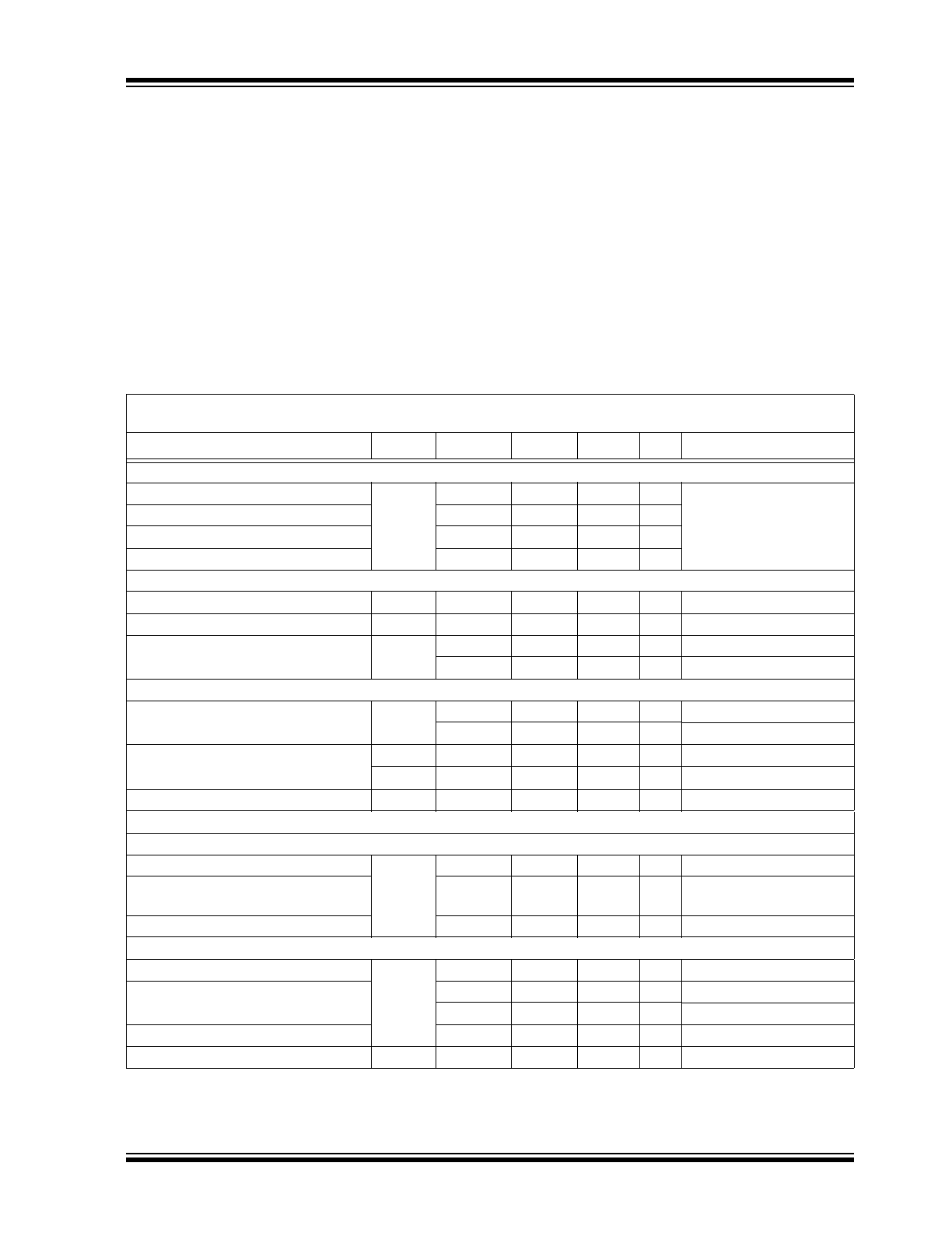
DC CHARACTERISTICS
Electrical Specifications: Unless otherwise indicated,
V
DD
= 2.7V to 5.5V, T
A
= -40°C to +125°C, and
GND = Ground.
Parameters
Sym
Min
Typ
Max
Unit
Conditions
Sensor Accuracy
T
A
= +25°C, +45°C
T
ACY
—
±0.5
—
°C
Note 1
0°C
≤ T
A
≤ +125°C
-3.5
±1
+3.5
°C
-20°C
≤ T
A
≤ +125°C
-4.5
±1
+4.5
°C
-40°C
≤ T
A
≤ +125°C
—
±2
—
°C
Power Supply
Operating Voltage
V
DD
2.7
—
5.5
V
Operating Current (MCP9509)
I
DD
—
30
50
µA
Operating Current (MCP9510)
I
DD
—
50
80
µA
OUTSET = GND or V
DD
—
100
165
µA
OUTSET = Unconnected
Hysteresis
Trip Point Hysteresis
T
HYST
—
+2
—
°C
HYST = GND
—
+10
—
°C
HYST = V
DD
Hysteresis Select:
Input (HYST) Thresholds
V
IH
V
DD
- 0.4
—
—
V
V
IL
—
—
0.4
V
Hysteresis Input (HYST) Leakage
I
Leak
—
1
—
µA
MCP9510 Output Control Input (OUTSET Input)
OUTSET Input Voltage Threshold and Output Configuration
Push-Pull, Active Low
V
OSET
GND
—
0.2V
DD
V
Open-Drain with R
OUT
, Active
Low
0.45V
DD
—
0.7V
DD
V
or OUTSET Unconnected
Push-Pull, Active High
0.85V
DD
—
V
DD
V
OUTSET Input Leakage and Output Configuration
Push-Pull, Active Low
I
Leak
—
10
—
µA
GND
≤ V
OSET
≤ 0.2V
DD
Open-Drain, Active Low
—
0
—
µA
Unconnected (i.e. open)
—
7
—
µA
0.4V
DD
≤ V
OSET
≤ 0.7V
DD
Push-Pull, Active High
—
-10
—
µA
0.85
≤ V
OSET
≤ V
DD
OUTSET Input Impedance
Z
OUTSET
—
500
—
k
Ω
Note 1: This specification is tested at mid supply of 4.1V for optimum operation across the supply voltage range of
2.7V to 5.5V.
MCP9509/10
DS22114A-page 4
© 2008 Microchip Technology Inc.
Outputs
(OUT, OUT)
Output Voltage High, MCP9510
V
OH
V
DD
- 0.55
—
V
DD
V
I
OUT
= 5 mA
OUTSET = V
DD
or GND
Output Voltage Low, MCP9510
V
OL
GND
—
0.3
V
Output Voltage Low, MCP9509
V
OL
GND
—
0.3
V
I
OUT
= 5 mA
Internal Output Pull-up (MCP9510)
R
OUT
60
100
140
k
Ω OUTSET Unconnected
Open-Drain Output Leakage
I
Leak
—
1
—
µA
MCP9509/10
Power Supply Rejection
PSR
—
0.05
—
°C/V
Thermal Response
SOT23-5, SOT23-6
t
RES
—
1.7
—
s
Time to 63% (88°C).
+25°C (Air) to +125°C
(oil bath)
DC CHARACTERISTICS (CONTINUED)
Electrical Specifications: Unless otherwise indicated,
V
DD
= 2.7V to 5.5V, T
A
= -40°C to +125°C, and
GND = Ground.
Parameters
Sym
Min
Typ
Max
Unit
Conditions
Note 1: This specification is tested at mid supply of 4.1V for optimum operation across the supply voltage range of
2.7V to 5.5V.
TEMPERATURE CHARACTERISTICS
Electrical Specifications: Unless otherwise indicated,
V
DD
= 2.7V to 5.5V, T
A
= -40°C to +125°C, and
GND = Ground.
Parameters
Sym
Min
Typ
Max
Units
Conditions
Temperature Ranges
Specified Temperature Range
T
A
-40
—
+125
°C
(Note 1)
Operating Temperature Range
T
A
-40
—
+125
°C
Storage Temperature Range
T
A
-65
—
+150
°C
Thermal Package Resistances
Thermal Resistance, 5L-SOT23
θ
JA
—
220.7
—
°C/
Ω
Thermal Resistance, 6L-SOT23
θ
JA
—
190.5
—
°C/
Ω
Note 1: Operation in this range must not cause T
J
to exceed Maximum Junction Temperature (+150°C).
© 2008 Microchip Technology Inc.
DS22114A-page 5
MCP9509/10
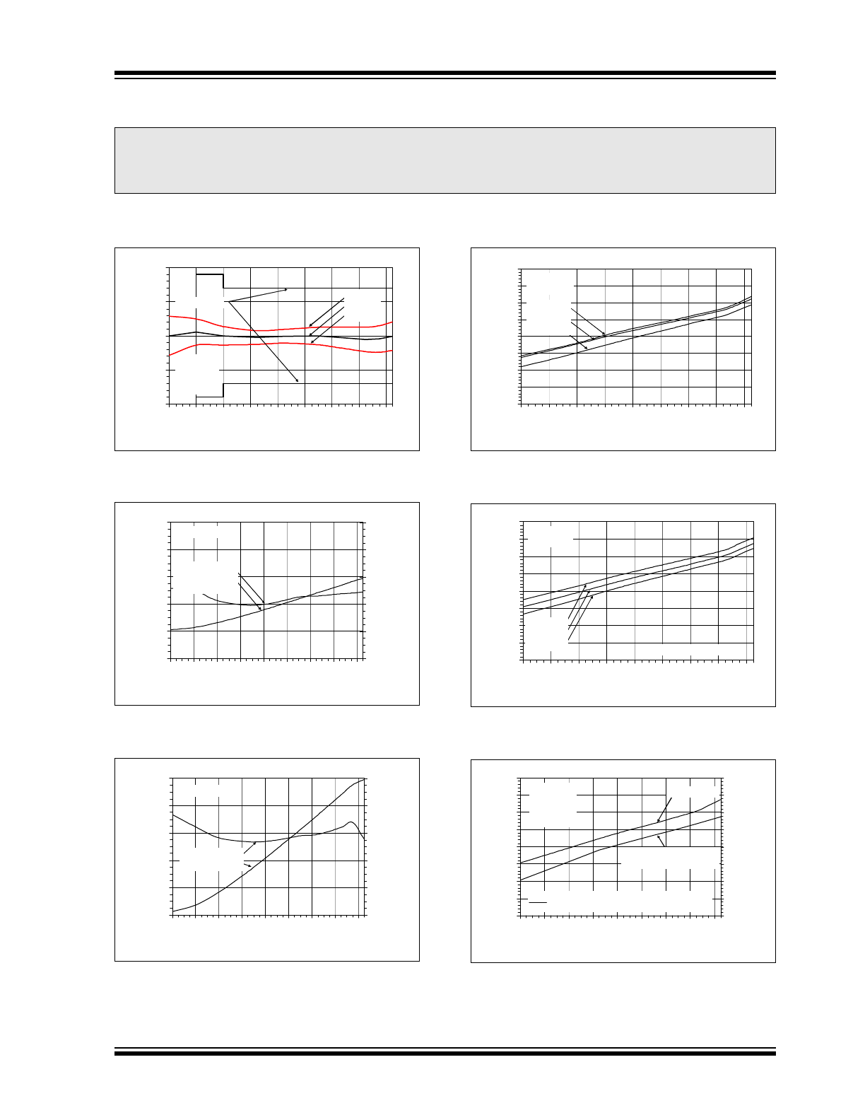
2.0
TYPICAL PERFORMANCE CURVES
Note: Unless otherwise indicated, V
DD
= 2.7V to 5.5V, T
A
= -40°C to +125°C, GND = Ground, R
PULL-UP
= 10 k
Ω
(MCP9509 only) and 0.1 µf bypass capacitor.
FIGURE 2-1:
Temperature Accuracy.
FIGURE 2-2:
Output Hysteresis vs.
Temperature.
FIGURE 2-3:
Output Hysteresis vs.
Temperature.
FIGURE 2-4:
Supply Current vs.
Temperature (MCP9509).
FIGURE 2-5:
Supply Current vs.
Temperature OUTSET = V
DD
, V
SS
(MCP9510).
FIGURE 2-6:
Supply Current vs.
Temperature OUTSET = Unconnected, Open
(MCP9510).
Note:
The graphs and tables provided following this note are a statistical summary based on a limited number of
samples and are provided for informational purposes only. The performance characteristics listed herein
are not tested or guaranteed. In some graphs or tables, the data presented may be outside the specified
operating range (e.g., outside specified power supply range) and therefore outside the warranted range.
-5.0
-2.5
0.0
2.5
5.0
-40
-20
0
20
40
60
80
100 120
Temperature (°C)
T
e
m
p
er
atu
re A
c
cu
ra
cy (
°C
)
Spec. Limit
MCP9509C
MCP9509H
MCP9510C
MCP9510H
+ σ
Average
- σ
0.0
1.0
2.0
3.0
4.0
5.0
-40 -20
0
20
40
60
80 100 120
Temperature (°C)
H
y
s
ter
esi
s (
°C
)
0.0
1.0
2.0
3.0
4.0
5.0
H
yster
e
s
is
(k
Ω
)
Hysteresis (kΩ)
Hysteresis (°C)
HYST = GND
5.0
7.0
9.0
11.0
13.0
15.0
-40 -20
0
20
40
60
80 100 120
T
A
(°C)
H
ys
ter
es
is
(°
C
)
5.0
6.0
7.0
8.0
9.0
10.0
H
y
st
e
res
is
(
k
Ω
)
Hysteresis (kΩ)
Hysteresis (°C)
HYST = V
DD
10
15
20
25
30
35
40
45
50
-40
-20
0
20
40
60
80
100
120
Temperature (°C)
S
upp
ly
C
u
rr
e
n
t,
I
DD
(µ
A
)
V
DD
= 5.5V
V
DD
= 4.1V
V
DD
= 2.7V
MCP9509C
MCP9509H
10
15
20
25
30
35
40
45
50
-40
-20
0
20
40
60
80
100
120
Temperature (°C)
S
u
p
p
ly C
u
rr
en
t,
I
DD
(µA)
V
DD
= 5.5V
V
DD
= 4.1V
V
DD
= 2.7V
MCP9510C
MCP9510H
OUTSET = V
DD
, V
SS
10
15
20
25
30
35
40
45
50
-40 -20
0
20
40
60
80 100 120
Temperature (°C)
I
DD
(µ
A)
,
De
-As
s
e
rte
d
70
75
80
85
90
95
100
105
110
I
DD
(
µ
A)
, As
s
e
rte
d
MCP9510C
MCP9510H
V
DD
= 4.0V
Asserted,
Internal Pull-Up Current
De-Asserted
OUTSET = Open
OUT = Open-Drain Output with Internal Pull-
MCP9509/10
DS22114A-page 6
© 2008 Microchip Technology Inc.
Note: Unless otherwise indicated, V
DD
= 2.7V to 5.5V, T
A
= -40°C to +125°C, GND = Ground, R
PULL-UP
= 10 k
Ω
(MCP9509 only) and 0.1 µf bypass capacitor.
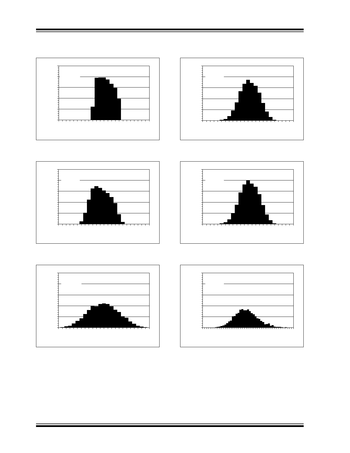
FIGURE 2-7:
Temperature Accuracy
Histogram at +45°C.
FIGURE 2-8:
Temperature Accuracy
Histogram at +70°C.
FIGURE 2-9:
Temperature Accuracy
Histogram at +125°C.
FIGURE 2-10:
Temperature Accuracy
Histogram at 0°C.
FIGURE 2-11:
Temperature Accuracy
Histogram at -20°C.
FIGURE 2-12:
Temperature Accuracy
Histogram at -40°C.
0%
4%
8%
12%
16%
20%
-3
.0
-2
.0
-1
.0
0.
0
1.
0
2.
0
3.
0
Temperature Accuracy (°C)
O
c
c
u
rr
en
ce
s
T
A
= +45°C
V
DD
= 4.1V
9087 Units
6 Lots
0%
4%
8%
12%
16%
20%
-3
.0
-2
.0
-1
.0
0.
0
1.
0
2.
0
3.
0
Temperature Accuracy (°C)
O
ccu
rr
e
n
ces
T
A
= +70°C
V
DD
= 4.1V
9280 Units
6 Lots
0%
4%
8%
12%
16%
20%
-3
.0
-2.
0
-1.
0
0.
0
1.
0
2.
0
3.
0
Temperature Accuracy (°C)
O
c
cu
rr
e
n
ce
s
T
A
= +125°C
V
DD
= 4.1V
9083 Units
6 Lots
0%
4%
8%
12%
16%
20%
-3
.0
-2
.0
-1
.0
0.
0
1.
0
2.
0
3.
0
Temperature Accuracy (°C)
O
ccu
rr
e
n
ces
T
A
= 0°C
V
DD
= 4.1V
8936 Units
6 Lots
0%
4%
8%
12%
16%
20%
-3
.0
-2
.0
-1
.0
0.
0
1.
0
2.
0
3.
0
Temperature Accuracy (°C)
O
ccu
rr
e
n
ces
T
A
= -20°C
V
DD
= 4.1V
8304 Units
6 Lots
0%
4%
8%
12%
16%
20%
-6
.0
-5.
0
-4.
0
-3
.0
-2.
0
-1.
0
0.
0
1.
0
2.
0
3.
0
4.
0
5.
0
6.
0
Temperature Accuracy (°C)
O
c
cu
rr
e
n
ce
s
T
A
= -40°C
V
DD
= 4.1V
9412 Units
6 Lots
© 2008 Microchip Technology Inc.
DS22114A-page 7
MCP9509/10
Note: Unless otherwise indicated, V
DD
= 2.7V to 5.5V, T
A
= -40°C to +125°C, GND = Ground, R
PULL-UP
= 10 k
Ω
(MCP9509 only) and 0.1 µf bypass capacitor.
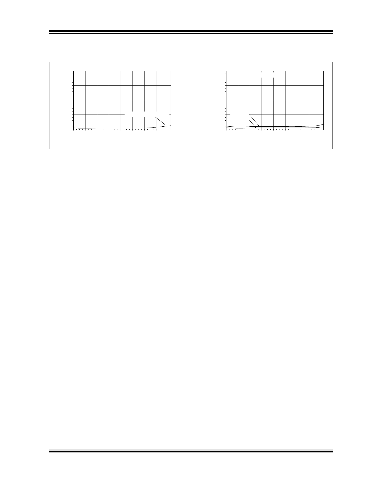
FIGURE 2-13:
Hysteresis Input Leakage
vs, Temperature.
FIGURE 2-14:
Output Leakage vs.
Temperature.
0
0.25
0.5
0.75
1
-40
-20
0
20
40
60
80
100 120
Temperature (°C)
L
eak
ag
e (
µ
A
)
Hysteresis Input Leakage
0
0.25
0.5
0.75
1
-40
-20
0
20
40
60
80
100 120
Temperature (°C)
O
u
tp
u
t L
eak
ag
e (
µ
A
)
MCP9509 Output Leakage
V
DD
= 5.5V
V
DD
= 2.7V

MCP9509/10
DS22114A-page 8
© 2008 Microchip Technology Inc.
NOTES:
© 2008 Microchip Technology Inc.
DS22114A-page 9
MCP9509/10
3.0
PIN DESCRIPTIONS
TABLE 3-1:
PIN FUNCTION TABLE
3.1
External Resistor Input (SET)
This pin is used to connect a resistor between the SET
and GND pins to select the temperature trip point
(T
SET
). The resistor value can be determined either
from
Equation 4-2
or the lookup table shown in
Table 4-2
.
3.2
Ground (GND)
The GND pin is the system ground pin.
3.3
Hysteresis Input (HYS)
This is an input pin which can be connected to V
DD
or
GND to select output hysteresis. Either 2°C
(HYS = GND) or 10°C (HYS = V
DD
)
of hysteresis can
be selected.
3.4
Power Pin (V
DD
)
The operating voltage range, as specified in the DC
electrical specification table, is applied on this pin.
3.5
Open-Drain Output (OUT)
(MCP9509)
This output is triggered when temperature exceeds the
programmed trip temperature. This pin requires a
pull-up resistor.
3.6
Selectable Output (OUT, OUT)
(MCP9510)
The output pin can be configured as either a Push-Pull
Active-High, Push-Pull Active-Low, or an Open-drain
Output with an internal pull-up resistor. The three
output options of the MCP9510 are selected by the
OUTSET pin.
3.7
Output Control (OUTSET)
(MCP9510)
The OUTSET pin is used to select the desired
configuration of the OUT or OUT pin.
TABLE 3-1:
OUTSET SELECTABLE
OUTPUTS
MCP9509 MCP9510
Symbol
Description
SOT-23-5
SOT-23-6
1
1
SET
External Trip Temperature Resistor (R
SET
) input
2
2
GND
Ground
3
—
OUT
Open-drain output
—
3
OUT,
OUT
Selectable Output pin,
function set by OUTSET pin
4
4
HYS
Hysteresis Input
HYS = GND, hysteresis is 2°C
HYS = V
DD
, hysteresis is 10°C
5
6
V
DD
Power pin
—
5
OUTSET Output Control
OUTSET = GND, Active-Low, Push-Pull
OUTSET = V
DD
, Active-High, Push-Pull
OUTSET = Unconnected, Active-Low, Open-Drain with an internal pull-up
OUTSET Pin
OUT / OUT Pin
GND
Push-Pull, Active-Low
V
DD
Push-Pull, Active-High
unconnected
(i.e. open)
Open-Drain output with an
internal pull-up resistor of
100 k
Ω (typical)

MCP9509/10
DS22114A-page 10
© 2008 Microchip Technology Inc.
NOTES: