
2013 - 2017 Microchip Technology Inc.
DS20005172C-page 1
RE46C800
Features
• Low Quiescent Current
• Operation from 2V or 12V
• 9.8V Boost Regulator
• Horn Driver
• LED Driver
• 3.3V Regulated Voltage for Microcontroller
Operation
• Internal Operational Amplifiers:
- ±1 mV Input Offset Voltage
- Rail-to-Rail Input and Output
- 10 kHz Gain Bandwidth Product
- Unity Gain Stable
• Bidirectional Alarm Interconnect
Applications
• CO Detector
• Toxic Gas Detector
• Heat Detector
Description
The RE46C800 is a low power CMOS carbon monoxide
detector companion IC. The RE46C800 provides all of
the analog, interface, and power management functions
for a microcontroller-based CO or toxic gas detector. It
is intended for use in both 3V and 9V battery or battery-
backed applications. It features a boost regulator and
horn driver circuit suitable for driving a piezoelectric
horn, a 3.3V regulator for microcontroller voltage
regulation, an LED driver, an operational amplifier and
an IO for communication with interconnected units.
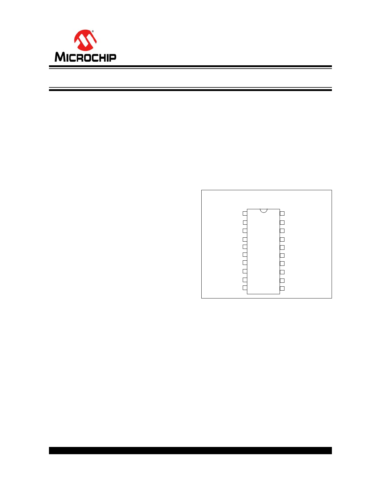
Package Types
1
2
3
4
20
19
18
17
V
DD
INP
V
SS
LX
HRNEN
HB
HS
FEED
RE46C800
SSOP
5
6
7
8
9
10
INN
V
REF
OPOUT
9VDET
ACDET
LEDEN
IO1
IO2
16
15
14
13
12
11
LEDPWR
V
BST
V
REG
IODIR
Carbon Monoxide Detector Companion IC
RE46C800
DS20005172C-page 2
2013 - 2017 Microchip Technology Inc.
Functional Block Diagram
LEDEN (8)
HRNEN (20)
V
SS
(16)
LX (15)
V
BST
(13)
HS (18)
LEDPWR (14)
HB (19)
V
REG
(12)
V
REF
(3)
FEED (17)
LEVEL
SHIFTER
V
BST
V
DDS
9VDET (5)
BOOST
DISABLE
IODIR (11)
OV
Protection
V
REF
GENERATOR
V
DD
(6)
V
REG
V
DDS
ACDET (7)
REFERENCE
VOLTAGE
SUPPLY
SELECT
I_LIMIT
PWM
CONTROL
ERROR
AMPLIFIER
IO2 (10)
IO1 (9)
INTERCONNECT
V
BST
INN (2)
INP (1)
OPOUT (4)
V
REG
V
DDS

2013 - 2017 Microchip Technology Inc.
DS20005172C-page 3
RE46C800
1.0
ELECTRICAL
CHARACTERISTICS
1.1
Absolute Maximum Ratings†
V
DD
............................................................................................................................................................... -0.3V to 5.5V
ESD HBM................................................................................................................................................................1500V
ESD MM....................................................................................................................................................................150V
V
BST
, LX........................................................................................................................................................ -0.3V to 13V
Input Voltage Range Except ACDET, 9VDET, FEED, IO1 ..................................................... V
IN1
= – .3V to V
REG
+ .3V
ACDET, 9VDET Input Voltage Range .....................................................................................V
IN2
= – .3V to V
BST
+ .3V
FEED Input Voltage Range ........................................................................................................... V
INFD
= -10V to + 22V
IO1 Input Voltage Range....................................................................................................................V
INIO1
= -.3 to +15V
Input Current except FEED............................................................................................................................. I
IN
= 10 mA
Operating Temperature .....................................................................................................................T
A
= -10
C to +60C
Storage Temperature ..................................................................................................................T
STG
= -55
C to +125C
Maximum Junction Temperature ....................................................................................................................T
J
= +15
C
† Notice: Stresses above those listed under “Maximum Ratings” may cause permanent damage to the device. This
is a stress rating only and functional operation of the device at these or any other conditions above those indicated in
the operation listings of this specification is not implied. Exposure to maximum rating conditions for extended periods
may affect device reliability.
DC ELECTRICAL CHARACTERISTICS – RE46C800
Unless otherwise indicated, all parameters apply at T
A
= -10°C to +60°C, V
DD
= 3V, V
SS
= 0V, C
REG
= 10 µF,
C
BST
= 10 µF, 9VDET low, ACDET low. (
Note 1
) (
Note 2
) (
Note 3
)
Parameter
Symbol
Test
Pin
Min.
Typ.
Max.
Units
Conditions
Supply Voltage
V
DD
6
2
—
5
V
Operating
V
BST
13
6
—
12
V
Operating, 9V operation,
9VDET or ACDET high
Standby Supply Current I
DDSTBY1
—
13.6
—
µA
Inputs low; No loads, boost
regulator running (
Note 4
)
I
DDSTBY2
—
5.8
9.3
µA
Inputs low; No loads, boost
regulator disabled, 9V opera-
tion, V
BST
= 9V, 9VDET high
Quiescent Supply
Current
I
DDQ
6
—
6.8
10.3
µA
Inputs low; No loads;
V
BST
= 5V; V
LX
= 0.5V
Quiescent I
VO
I
VOQ
13
—
3.6
5.2
µA
Inputs low; No loads;
V
BST
= 5V; V
LX
= 0.5V
Note 1:
Wherever a specific V
BST
value is listed under test conditions, the V
BST
is forced externally with the inductor
disconnected and the boost regulator is NOT running.
2:
Typical values are for design information only.
3:
The limits shown are 100% tested at 25
°
C only. Test limits are guard-banded based on temperature characterization to
warrant compliance at temperature extremes.
4:
The Standby Supply Current I
DDSTBY1
specified above can be approximated as follows:
I
DDSTBY1
= I
DDQ
+ I
IND
Where I
DDQ
= average current into V
DD
supply
I
IND
= average inductor current = V
BST
* IVOQ/(V
IN
* Efficiency)
V
IN
= V
DD
= 3V

RE46C800
DS20005172C-page 4
2013 - 2017 Microchip Technology Inc.
Input Leakage Low
I
IL
1, 5, 7,
8, 10,
11, 20
—
—
-100
nA
INP, 9VDET, ACDET, LEDEN,
IO2, IODIR, HRNEN Inputs
V
IN
= V
SS
I
ILOP
2
—
—
-200
pA
INN input, V
IN
= V
SS
I
ILF
17
—
-15
-50
µA
FEED = -10V, V
BST
= 10V
Input Leakage High
I
IH1
1, 8,
10, 11,
20
—
—
100
nA
INP, LEDEN, IO2, IODIR,
HRNEN Inputs V
IN
= V
REG
I
IH2
5, 7
—
—
100
nA
9VDET, ACDET Inputs,
V
IN
= V
BST
, V
BST
= 10V.
I
IHOP
2
—
—
200
pA
INN input, V
IN
= V
REG
I
IHF
17
—
20
50
µA
FEED = +22V; V
BST
= 10V
Output Off Leakage
High
I
IHOZ
14, 15
—
—
1
µA
LEDEN = V
SS
, LEDPWR,
LX = V
BST
= 10V
Input Voltage Low
V
IL1
8, 10,
11, 20
—
—
1
V
LEDEN, IO2, IODIR, HRNEN
Inputs
V
IL2
7
—
—
7
V
ACDET Input, V
BST
= 10V
V
IL3
5
—
—
4
V
9VDET Input, V
BST
= 10V
V
ILF
17
—
—
3
V
FEED Input; V
BST
= 10V
V
ILIO
1
9
—
—
0.8
V
Falling edge of IO1 input,
IODIR = V
SS
Input Voltage High
V
IH1
8, 10,
11, 20
V
REG
-.7
—
—
V
LEDEN, IO2, IODIR, HRNEN
Inputs
V
IH2
7
8.2
—
—
V
ACDET Input, V
BST
= 10V
V
IH3
5
6
—
—
V
9VDET Input, V
BST
= 10V
V
IHF
17
7
—
—
V
FEED Input; V
BST
= 10V
V
IHIO
1
9
2
—
—
V
Rising edge of IO1 input,
IODIR = V
SS
Output Voltage Low
V
OL1
18, 19
—
—
0.5
V
HS or HB; I
OUT
= 16 mA;
V
DD
= 3V; V
BST
= 10V,
HRNEN = V
SS
V
OL2
14
—
—
0.5
V
LEDPWR; I
OUT
= 10 mA;
V
BST
= 10V
V
OLIO2
10
—
—
0.5
V
IO2 output, I
OUT
= 100 µA,
IODIR = V
SS
DC ELECTRICAL CHARACTERISTICS – RE46C800 (CONTINUED)
Unless otherwise indicated, all parameters apply at T
A
= -10°C to +60°C, V
DD
= 3V, V
SS
= 0V, C
REG
= 10 µF,
C
BST
= 10 µF, 9VDET low, ACDET low. (
Note 1
) (
Note 2
) (
Note 3
)
Parameter
Symbol
Test
Pin
Min.
Typ.
Max.
Units
Conditions
Note 1:
Wherever a specific V
BST
value is listed under test conditions, the V
BST
is forced externally with the inductor
disconnected and the boost regulator is NOT running.
2:
Typical values are for design information only.
3:
The limits shown are 100% tested at 25
°
C only. Test limits are guard-banded based on temperature characterization to
warrant compliance at temperature extremes.
4:
The Standby Supply Current I
DDSTBY1
specified above can be approximated as follows:
I
DDSTBY1
= I
DDQ
+ I
IND
Where I
DDQ
= average current into V
DD
supply
I
IND
= average inductor current = V
BST
* IVOQ/(V
IN
* Efficiency)
V
IN
= V
DD
= 3V
2013 - 2017 Microchip Technology Inc.
DS20005172C-page 5
RE46C800
Output Voltage High
V
OH1
18, 19
9.5
—
—
V
HS or HB; I
OUT
= -16 mA;
V
BST
= 10V; HRNEN = V
REG
V
OHIO1
9
3
—
—
V
IO1, I
OUT
= -4 mA,
IODIR = V
IH1
, IO2 = V
IH1
V
OHIO2
10
V
REG
-.5
—
—
V
IO2, I
OUT
= -100 µA,
IODIR = V
SS
, IO1 = V
IHIO1
Reference Voltage
V
REF
3
—
300
—
mV
V
BST
Output Voltage
V
VO1
13
9
9.8
10.6
V
V
DD
= 3V; HRNEN = V
REG
;
I
OUT
= 10 mA
V
VO2
13
3.6
4
4.4
V
V
DD
= 3V; HRNEN = V
SS;
I
OUT
=10 mA
V
BST
Efficiency
V
EFF1
—
85
—
%
I
LOAD
=10 mA; V
DD
=3V;
HRNEN = V
SS
V
EFF2
—
75
—
%
I
LOAD
= 100 µA; V
DD
= 3V;
HRNEN = V
SS
V
REG
Voltage
V
REG
12
3.2
3.3
3.4
V
I
OUT
< 20 mA
V
REG
Load Regulation
V
REGLD
12
—
30
50
mV
I
OUT
= 0 to 20 mA;
HRNEN = V
REG
Brown-out Threshold
V
OBVT
13
3.2
3.6
4
V
Falling edge of V
BST
V
BST
-to-Brown-out
Margin
V
OBVTM
13
100
400
—
mV
V
VO2
- V
OBVT
Brown-out Pull Down
I
BT
12
20
40
—
mA
V
BST
= 3.0V; V
REG
= 2.0V
V
REG
Over Voltage
Clamp
V
CL
12
3.75
4
4.25
V
IO1 Output Current
IO1
IH1
9
25
—
60
µA
IODIR = V
SS
, IO1 = 1V
IO1
IH2
9
—
—
150
µA
IODIR = V
SS
, IO1 = 15V
IO1
IOH1
9
-4
-5
—
mA
IODIR, IO2 = V
IH1
, IO1 = 3V
IO1
IOH2
9
—
-5
-16
mA
IODIR, IO2 = V
IH1
, IO1 = V
SS
IO1
IOL1
9
—
10
—
mA
IO Dump Current,
IODIR = V
IH1
, IO2 = V
SS
,
IO1 = 1V
IO1 Hysteresis
V
HYSTIO1
9
—
150
—
mV
IODIR = V
SS
Op Amp
Input Offset Voltage
V
OS
4
-1
—
1
mV
V
CM
= 0.3V
Common Mode Input
Range
V
CMR
1, 2
V
SS
—
V
REG
V
DC ELECTRICAL CHARACTERISTICS – RE46C800 (CONTINUED)
Unless otherwise indicated, all parameters apply at T
A
= -10°C to +60°C, V
DD
= 3V, V
SS
= 0V, C
REG
= 10 µF,
C
BST
= 10 µF, 9VDET low, ACDET low. (
Note 1
) (
Note 2
) (
Note 3
)
Parameter
Symbol
Test
Pin
Min.
Typ.
Max.
Units
Conditions
Note 1:
Wherever a specific V
BST
value is listed under test conditions, the V
BST
is forced externally with the inductor
disconnected and the boost regulator is NOT running.
2:
Typical values are for design information only.
3:
The limits shown are 100% tested at 25
°
C only. Test limits are guard-banded based on temperature characterization to
warrant compliance at temperature extremes.
4:
The Standby Supply Current I
DDSTBY1
specified above can be approximated as follows:
I
DDSTBY1
= I
DDQ
+ I
IND
Where I
DDQ
= average current into V
DD
supply
I
IND
= average inductor current = V
BST
* IVOQ/(V
IN
* Efficiency)
V
IN
= V
DD
= 3V

RE46C800
DS20005172C-page 6
2013 - 2017 Microchip Technology Inc.
Common Mode
Rejection Ratio
CMRR
1, 2, 4
—
80
—
dB
V
REG
= 3.3V, VCM = -0.3V to
3.3V
DC Open-Loop Gain
(large signal)
A
OL
4
—
115
—
dB
RL = 50 kΩ, V
OUT
= 0.3V to
V
REG
- 0.3V
Maximum Output
Voltage Swing
V
OL
, V
OH
4
V
SS
+10
—
V
REG
-10
mV
RL = 50 kΩ, 0.5V input
overdrive
Output Short Circuit
Current
I
SC
4
—
20
—
mA
V
REG
= 3.3V
DC ELECTRICAL CHARACTERISTICS – RE46C800 (CONTINUED)
Unless otherwise indicated, all parameters apply at T
A
= -10°C to +60°C, V
DD
= 3V, V
SS
= 0V, C
REG
= 10 µF,
C
BST
= 10 µF, 9VDET low, ACDET low. (
Note 1
) (
Note 2
) (
Note 3
)
Parameter
Symbol
Test
Pin
Min.
Typ.
Max.
Units
Conditions
Note 1:
Wherever a specific V
BST
value is listed under test conditions, the V
BST
is forced externally with the inductor
disconnected and the boost regulator is NOT running.
2:
Typical values are for design information only.
3:
The limits shown are 100% tested at 25
°
C only. Test limits are guard-banded based on temperature characterization to
warrant compliance at temperature extremes.
4:
The Standby Supply Current I
DDSTBY1
specified above can be approximated as follows:
I
DDSTBY1
= I
DDQ
+ I
IND
Where I
DDQ
= average current into V
DD
supply
I
IND
= average inductor current = V
BST
* IVOQ/(V
IN
* Efficiency)
V
IN
= V
DD
= 3V
2013 - 2017 Microchip Technology Inc.
DS20005172C-page 7
RE46C800
AC ELECTRICAL CHARACTERISTICS
Unless otherwise indicated, all parameters apply at T
A
= -10°C to +60°C, V
DD
= 3V, V
SS
= 0V, C
REG
= 10 µF,
C
VBST
= 10 µF.
Parameter
Symbol Test Pin
Min.
Typ.
Max.
Units
Conditions
OP Amp AC Response
Gain Bandwidth
Product
GBWP
4
—
10
—
kHz
Slew Rate
SR
4
—
3
—
V/ms
Phase margin
PM
4
—
65
—
°
G = +1V/V
Op Amp Noise
Input Voltage
Noise
E
ni
1, 2
—
5
—
µV
P-P
f = 0.1 Hz to 10 kHz
Input Voltage
Noise Density
e
ni
1, 2
—
170
—
nV/
√Hz
f = 1 kHz
Input Current
Noise Density
i
ni
1, 2
—
0.6
—
fA/
√Hz
f = 1 kHz
Note 1:
Wherever a specific V
BST
value is listed under test conditions, the V
BST
is forced externally with the inductor
disconnected and the boost regulator is NOT running.
2:
Typical values are for design information only.
3:
The limits shown are 100% tested at 25
°
C only. Test limits are guard-banded based on temperature characterization to
warrant compliance at temperature extremes.
TEMPERATURE CHARACTERISTICS
Electrical Characteristics: Unless otherwise indicated, V
DD
= 3V, V
SS
= 0V
Parameter
Sym.
Min.
Typ.
Max.
Units
Conditions
Temperature Ranges
Operating Temperature Range
T
A
-10
—
60
°C
Storage Temperature Range
T
STG
-55
—
125
°C
Thermal Package Resistances
Thermal Resistance, 20L-SSOP
JA
—
87.3
—
°C/W

RE46C800
DS20005172C-page 8
2013 - 2017 Microchip Technology Inc.
2.0
PIN DESCRIPTIONS
The descriptions of the pins are listed in
Table 2-1
.
TABLE 2-1:
PIN FUNCTION TABLE
RE46C800
Symbol
Description
SSOP
1
INP
Noninverting input of the op amp.
2
INN
Inverting input of the op amp.
3
V
REF
Voltage reference for CO biasing and detection circuitry.
4
OPOUT
Output of the op amp.
5
9VDET
Logic input used to disable the boost regulator.
6
V
DD
Low-voltage supply input.
7
ACDET
AC power detect pin.
8
LEDEN
Logic input used to enable the LED driver. Input is designed to interface with
circuitry supplied by V
REG
, so input voltage levels will scale with the V
REG
voltage.
9
IO1
Logic bidirectional pin used for connection to remote units. This pin has an
internal pull-down device. If used as an output, high level is VVO1.
10
IO2
Bidirectional pin used to send and receive IO1 interconnect signal status.
11
IODIR
Logic input used to select IO direction.
12
V
REG
Regulated output voltage. Nominal output is 3.3V.
13
V
BST
Boost regulator output, typically output voltage is 4V or 9.8V. Also used as
the high-voltage supply input.
14
LEDPWR
Open drain NMOS output used to drive a visible LED.
15
LX
Open drain NMOS output used to drive the boost regulator inductor. The
inductor should be connected from this pin to the positive supply through a
low resistance path.
16
V
SS
Connect to the negative supply voltage.
17
FEED
Usually connected to the feedback electrode of the piezoelectric horn
through a current limiting resistor. If not used, this pin must be connected to
V
SS
.
18
HS
HS is a complementary output to HB and connects to the ceramic electrode
(S) of the piezoelectric transducer.
19
HB
This pin is connected to the metal electrode (B) of a piezoelectric transducer.
20
HRNEN
Logic input for horn enable designed to interface with circuitry supplied by
V
REG
. Input voltage levels will scale with the V
REG
voltage.
2013 - 2017 Microchip Technology Inc.
DS20005172C-page 9
RE46C800
3.0
DEVICE DESCRIPTION
3.1
Introduction
The RE46C800 provides the necessary analog
functions to build a microcontroller-based CO or toxic
gas detector. This includes an op amp and voltage
reference for the electrochemical sensor, a voltage
regulator for the microcontroller, an LED driver, a horn
driver, a detector interconnect function, a boost regula-
tor for 3V operation, and a power management system
that allows operation from 3V, 9V or AC derived power.
The power management system provides the capability
for AC power with battery backup. The RE46C800
provides a simple means for the microcontroller to
control the operation of the CO detector and provide
the necessary signaling functions during an alarm
condition.
3.2
CO Sensor Circuit
The RE46C800 provides a low offset op amp and
reference voltage, V
REF
, for a two terminal
electrochemical CO or toxic gas sensor. The unity gain
stable op amp provides rail-to-rail inputs and output.
The op amp output is monitored by the microcontroller
to determine the CO concentration. This uncommitted
op amp can be used for other purposes such as
temperature sensing.
3.3
Power Management System
The power management system allows the RE46C800
to be powered from a 3V or 9V battery or AC power. AC
power is supplied as a DC voltage derived from an AC
power supply. This DC voltage is diode connected to
the V
BST
pin of the RE46C800. AC supplied power and
a 9V battery can both be diode connected to the V
BST
pin.
For low-voltage systems the battery is connected to the
V
DD
pin. When only a low-voltage battery is available,
the internal circuitry is powered from V
DD
. When a 9V
battery or AC power is available, the internal circuitry is
powered from V
REG
, which is a regulated 3.3V. The
selection of the power source for the internal circuitry is
controlled with the ACDET pin when the 9VDET pin is
low.
In low-voltage systems that are also AC powered, the
boost regulator will turn on if voltage of the AC supplied
power drops below the specified boost regulator
voltage. This can cause the low-voltage battery to
discharge more rapidly than expected.
The 9VDET pin will disable the boost regulator if
9VDET is high. For a low-voltage system, the 9VDET
pin should be connected to V
SS
which will enable the
boost regulator.
Table 3-1
shows the truth table for the power
management system.
3.4
Boost Regulator
The boost regulator only operates in low-voltage
applications. The boost regulator is a fixed off time
boost regulator with peak current limiting. In low-boost
operation the peak current is nominally 0.6A. In high-
boost operation the peak current is nominally 1.2A. The
boost regulator normally operates in Low-Boost mode,
which provides a nominal 4V output voltage on the
V
BST
pin. In High-Boost mode, the boost regulator
provides a nominal 9.8V on the V
BST
pin. The boost
regulator can be placed in High-Boost mode with
HORNEN, LEDEN, or IODIR and IO2 both asserted
high.
The brown-out threshold voltage is the V
BST
voltage at
which the voltage regulator and the horn will be
disabled. When the V
BST
voltage falls below the brown-
out threshold voltage of 3.6V, V
REG
will be disabled and
pulled to V
SS
with a nominal 40 mA current. When the
boost voltage rises above the brown-out threshold
voltage, V
REG
is enabled.
3.5
Voltage Regulator
The voltage regulator provides a nominal 3.3V output
at the V
REG
pin and is intended to power a
microcontroller. In normal operation, the regulator will
source current up to 20 mA, but the current sinking
capability is typically under 1 µA. The voltage regulator
is powered from the V
BST
pin. In low-voltage
applications the regulator is powered by the boost
regulator and the regulator load current is part of the
boost regulator load current. An overvoltage clamp is
intended to limit the voltage at V
REG
if it is pulled up by
an external source to greater than 4V. When the boost
regulator experiences a brown-out condition, the
voltage regulator will be disabled and the V
REG
output
will be pulled to V
SS
.
TABLE 3-1:
POWER MANAGEMENT
SYSTEM
9VDET ACDET
Internal
Supply
Boost Regulator
0
0
V
DD
Enabled
0
1
V
REG
Enabled
1
0
V
REG
Disabled
1
1
V
REG
Disabled

RE46C800
DS20005172C-page 10
2013 - 2017 Microchip Technology Inc.
3.6
LED Driver
The LED drive circuit provides power to an LED, which
can be used as a visual indicator by the system. The
LED drive circuit can also be used as part of a battery
check function in battery-powered applications. When
LEDEN is asserted high the LED will load the V
BST
output and the microcontroller can monitor the battery
operation under load. In low-voltage systems the boost
regulator will be placed into high-boost operation when
LEDEN is asserted high. The load current is set by the
resistor in series with the LED.
3.7
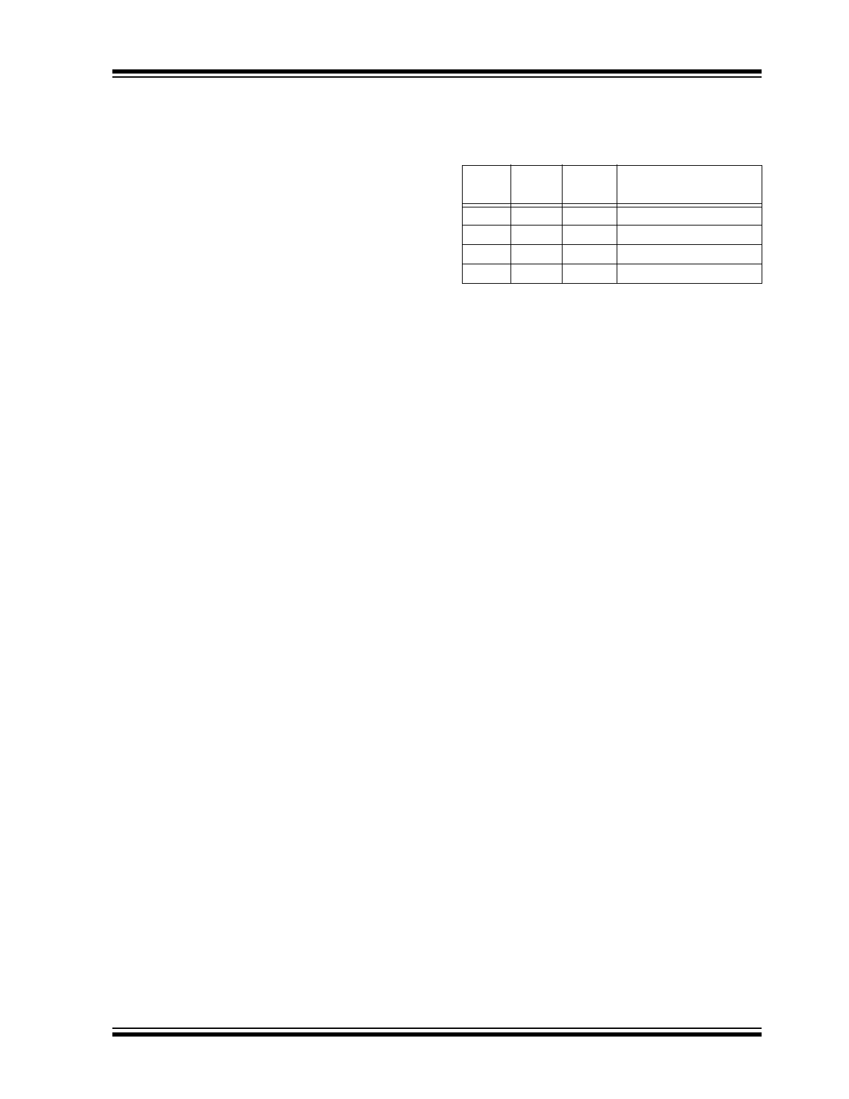
Interconnect Operation
The IO circuitry provides the means for the CO detector
to be connected to other CO detectors or smoke
alarms.
Table 3-2
below provides the truth table for the
interconnect circuit operation. IO1 is a bidirectional pin
that connects to other CO detectors or smoke alarms.
IO2 is a bidirectional pin that connects to the
microcontroller. IODIR connects to the microcontroller
and determines when IO1 and IO2 act as an input or
output. When IO1 is used as an output asserting a logic
high, the IO1 output acts as current source that is
biased from V
BST
. In low-voltage applications where
the boost regulator is enabled, the boost regulator will
operate in High-Boost mode. When IO1 is used as an
output asserting a logic low, the IO1 output acts as
current sink. IO2 logic levels are referenced to V
REG
.
TABLE 3-2:
INTERCONNECT LOGIC
TRUTH TABLE
IODIR
IO2
IO1
Input
Output
Input
Output
1
0
—
—
0
1
1
—
—
1
0
—
0
0
—
0
—
1
1
—