
2012-2013 Microchip Technology Inc.
DS20002301B-page 1
RE46C317/18
Features:
• 3V Operation
• Low Quiescent Current
• 10V Boost Converter
• Low Horn Driver On-Resistance
• Compatible with RE46C117
Applications:
• Smoke Detectors
• CO Detectors
• Personal Security Products
• Electronic Toys
Description:
The RE46C317/18 are CMOS piezoelectric horn driver
ICs with built-in boost converter. They are intended for
use in 3V battery or battery-backed applications. The
circuits feature a boost converter and a driver circuit
suitable for driving a piezoelectric horn.
The RE46C317/18 are compatible with the RE46C117
device and offer lower standby current.
The RE46C317 has three valid states of Horn Enable
(tri-state, low and high), while the RE46C318 has only
two valid states, low and high.
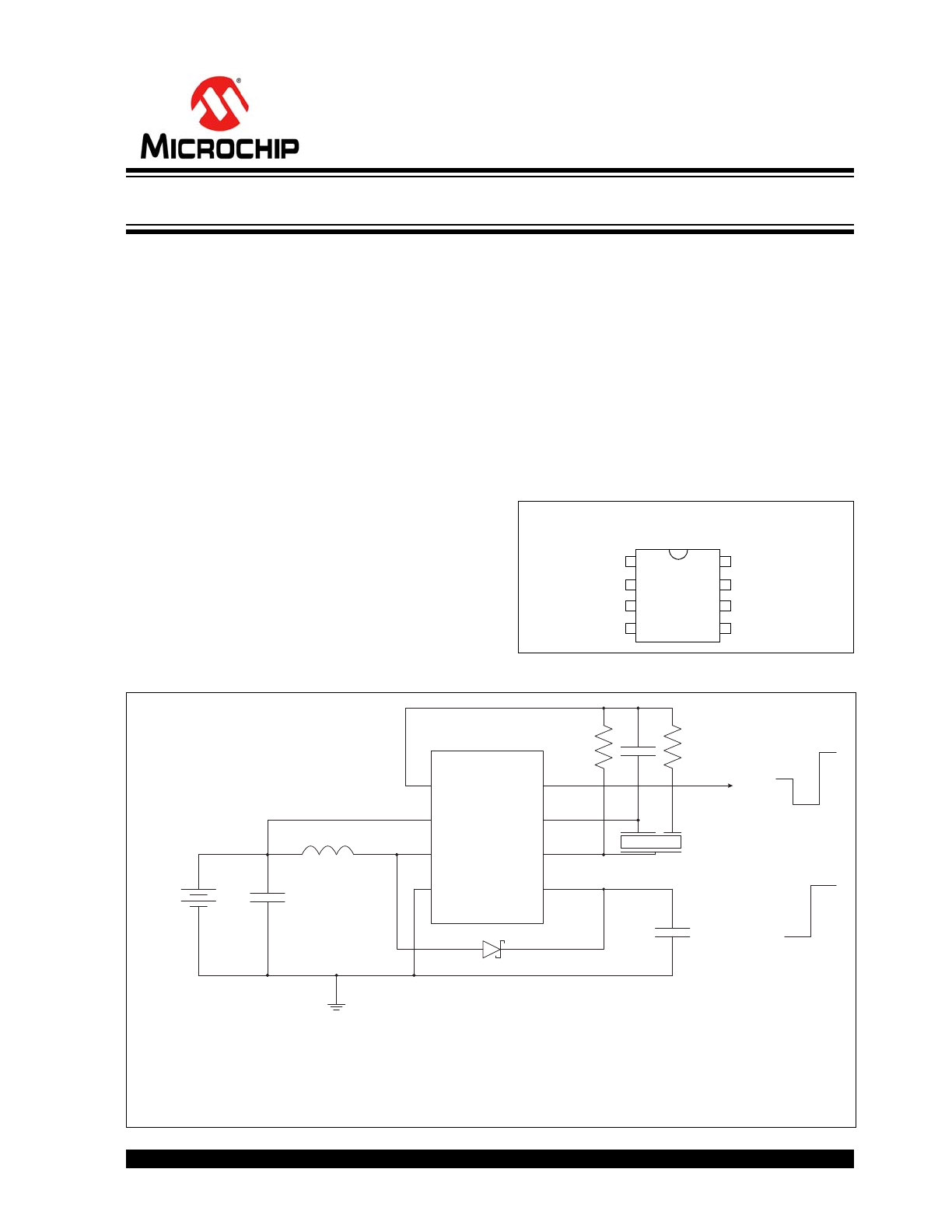
Package Types
Typical Application
1
2
3
4
8
7
6
5
V
DD
LX
V
SS
FEED
HRNEN
HORNS
HORNB
V
O
RE46C317/18
PDIP, SOIC
E
F ED
V
DD
HRNEN
HORNS
LX
V
SS
HORNB
V
O
RE46C317/18
2V to 5V
10 μF
10 μH
10 μF
1 nF
200K
1.5M
RE46C318 Only
Low
High
RE46C317 Only
Low
High
Tri-state
L
1
C
1
D
1
C
3
C
4
R
2
R
1
V
1
Note 1: Schottky diode D
1
must have the maximum peak current rating of at least 1A. For best results, the
forward voltage spec should be less than 0.5V at 1A.
2: Inductor L
3
must have the maximum peak current rating of at least 1A. For best results, the DC resistance
should be less than 0.5
.
Piezoelectric Horn Driver with Boost Converter
RE46C317/18
DS20002301B-page 2
2012-2013 Microchip Technology Inc.
Functional Block Diagram
Gate Control
Tri-state Logic
Level Shifter
(
RE46C317 Only)
Horn Driver
HRNEN
V
SS
LX
HORNS
HORNB
V
O
FEED
Standard Logic
Level Shifter
(
RE46C318 Only)
Voltage Reference
+
-
+
-
V
DD
R
1
R
2
R
3
2012-2013 Microchip Technology Inc.
DS20002301B-page 3
RE46C317/18
1.0
ELECTRICAL
CHARACTERISTICS
1.1
Absolute Maximum Ratings†
V
DD
............................................................................................................................................................................. 5.5V
V
OUT
......................................................................................................................................................................... 12.5V
Input Voltage Range Except FEED, LX................................................................................V
IN
= V
SS
– .3V to V
DD
+ .3V
FEED Input Voltage Range ........................................................................................................... V
INFD
= -10V to + 22V
LX Input Voltage ...............................................................................................................................V
INLX
= V
OUT
+ 0.8V
Input Current except FEED, LX ...................................................................................................................... I
IN
= 10 mA
LX Current (Peak) ...........................................................................................................................................I
INLX
= 1.0A
Operating Temperature ..................................................................................................................... T
A
= -10
C to +60C
Storage Temperature ..................................................................................................................T
STG
= -55
C to +125C
Continuous Operating Current (HORNS, HORNB, V
O
) .................................................................................. I
O
= 40 mA
Maximum Human Body Model ESD........................................................................................................................ 1500V
† Notice: Stresses above those listed under “Maximum ratings” may cause permanent damage to the device. This
is a stress rating only and functional operation of the device at these or any other conditions above those indicated in
the operation listings of this specification is not implied. Exposure to maximum rating conditions for extended periods
may affect device reliability. This product utilizes CMOS technology with static protection; however proper ESD
prevention procedures should be used when handling this product. Damage can occur when exposed to extremely
high static electrical charge.
DC ELECTRICAL CHARACTERISTICS – RE46C317
Unless otherwise indicated, all parameters apply at T
A
= -10°C to +60°C, V
DD
= 3V, V
SS
= 0V, C
3
= 10 µF.
Typical values are at T
A
= +25°C
Parameter
Symbol
Test
Pin
Min.
Typ.
Max.
Units
Conditions
Supply Voltage
V
DD
2
2
—
5
V
Operating
Standby Supply Current
I
DD1
2
—
0.5
1
µA
HRNEN = Float; No loads
Standby I
VO
I
VO1
5
—
0
0.3
µA
HRNEN = Float; No loads
Quiescent Supply Current
I
DD2
2
—
27
49
µA
HRNEN = Low; No Loads;
V
O
= 11V; V
L X
= 0.5V
Quiescent I
VO
I
VO2
5
—
71
115
µA
HRNEN = Low; No Loads;
V
O
= 11V; V
L X
= 0.5V
Supply current
I
SUP
2
—
300
—
µA
HRNEN = Low; No Loads,
Boost Running
Input Current for Tri-state
I
IT
8
-5
—
5
µA
HRNEN = Float (
Note 4
)
Input Voltage High
V
IHH
8
2.6
—
—
V
HRNEN input
V
IHF
1
7
—
—
V
FEED input; V
O
= 10V
Note
1:
The boost converter in Boost mode (normal V
O
= 10V) can draw current pulses of ~0.8A and therefore is very sensitive
to series resistance. The critical components of this resistance are the inductor DC resistance, the internal resistance of
the battery and the resistance in the connections from the inductor to the battery, from the inductor to the LX pin. In
order to function properly under full load at V
DD
= 2V, the total of the inductor and the interconnect resistances should
not exceed 0.3
. The internal battery resistance should be no more than 0.5. A low ESR capacitance of 10 µF or more
should be connected in parallel with the battery to average current over the boost converter cycle.
2:
In the above table, wherever a specific V
O
value is listed under test conditions, the V
O
is forced externally with the
inductor disconnected, and the boost converter is not running.
3:
The limits shown are 100% tested at +25°C only. Test limits are guard-banded, based on temperature characterization
to ensure compliance at temperature extremes.
4:
This is the maximum input current that will not cause a logic high or logic low to be asserted.
RE46C317/18
DS20002301B-page 4
2012-2013 Microchip Technology Inc.
Input Voltage Low
V
ILH
8
—
—
0.4
V
HRNEN input
V
ILF
1
—
—
3
V
FEED input; V
O
= 10V
Input Leakage
I
IHF
1
—
20
50
µA
FEED = 22V; V
O
= 10V
I
ILF
1
-50
-15
—
µA
FEED = -10V; V
O
= 10V
I
IHH
8
—
20
50
µA
HRNEN = V
DD
I
ILH
8
-50
-20
—
µA
HRNEN = V
SS
Output Leakage
I
OZH
3
—
—
1
µA
HRNEN = Float;
V
O
= 12.5V; V
LX
= 10V
V
O
Output Voltage
V
VO
5
9
10
11
V
V
DD
= 3V,
HRNEN = Low or High,
I
OUT
= 10 mA
V
O
Efficiency
V
OEFF
5
—
80
—
%
I
LOAD
= 10 mA,
V
DD
= 3V, HRNEN = 0V
Output Low Voltage
V
OL
6, 7
—
0.3
0.5
V
HORNB or HORNS
I
OUT
= -16 mA, V
DD
= 3V
Output High Voltage
V
OH
6, 7
9.5
9.7
—
V
HORNB or HORNS
V
O
=10V
V
DD
= HRNEN = 3V
I
OUT
= 16 mA
DC ELECTRICAL CHARACTERISTICS – RE46C317 (CONTINUED)
Unless otherwise indicated, all parameters apply at T
A
= -10°C to +60°C, V
DD
= 3V, V
SS
= 0V, C
3
= 10 µF.
Typical values are at T
A
= +25°C
Parameter
Symbol
Test
Pin
Min.
Typ.
Max.
Units
Conditions
Note
1:
The boost converter in Boost mode (normal V
O
= 10V) can draw current pulses of ~0.8A and therefore is very sensitive
to series resistance. The critical components of this resistance are the inductor DC resistance, the internal resistance of
the battery and the resistance in the connections from the inductor to the battery, from the inductor to the LX pin. In
order to function properly under full load at V
DD
= 2V, the total of the inductor and the interconnect resistances should
not exceed 0.3
. The internal battery resistance should be no more than 0.5. A low ESR capacitance of 10 µF or more
should be connected in parallel with the battery to average current over the boost converter cycle.
2:
In the above table, wherever a specific V
O
value is listed under test conditions, the V
O
is forced externally with the
inductor disconnected, and the boost converter is not running.
3:
The limits shown are 100% tested at +25°C only. Test limits are guard-banded, based on temperature characterization
to ensure compliance at temperature extremes.
4:
This is the maximum input current that will not cause a logic high or logic low to be asserted.
2012-2013 Microchip Technology Inc.
DS20002301B-page 5
RE46C317/18
DC ELECTRICAL CHARACTERISTICS
-
RE46C318
Unless otherwise indicated, all parameters apply at T
A
= -10°C to +60°C, V
DD
= 3V, V
SS
= 0V, C
3
= 10 µF.
Typical values are at T
A
= +25°C.
Parameter
Symbol
Test
Pin
Min.
Typ.
Max.
Units
Conditions
Supply Voltage
V
DD
2
2
—
5
V
Operating
Standby Supply Current
I
DD1
2
—
—
0.1
µA
HRNEN = Low; No loads
Input Voltage High
V
IHH
8
2.3
—
—
V
HRNEN input
V
IHF
1
7
—
—
V
FEED input; V
O
= 10V
Input Voltage Low
V
ILH
8
—
—
1
V
HRNEN input
V
ILF
1
—
—
3
V
FEED input; V
O
= 10V
Input Leakage
I
IHF
1
—
20
50
µA
FEED = 22V; V
O
= 10V
I
ILF
1
-50
-15
—
µA
FEED = -10V; V
O
= 10V
I
IN
8
-100
—
100
nA
HRNEN = V
DD
or V
SS
Output Leakage
I
OZH
3
—
—
1
µA
HRNEN = V
SS
,
V
O
= 12.5V,
V
LX
= 10V
V
O
Output Voltage
V
VO
5
9
10
11
V
V
DD
= 3V,
HRNEN = High,
I
OUT
= 10 mA
V
O
Efficiency
V
VOEFF
5
—
80
—
%
I
LOAD
= 10 mA,
V
DD
= 3V,
HRNEN = 0V
Output Low Voltage
V
OL
6, 7
—
0.3
0.5
V
HORNB or HORNS;
I
OUT
= -16 mA;
V
DD
= 3V
Output High Voltage
V
OH
6, 7
9.5
9.7
—
V
HORNB or HORNS;
V
O
= 10V;
V
DD
= HRNEN = 3V;
I
OUT
= 16 mA
AC ELECTRICAL CHARACTERISTICS
Unless otherwise indicated, all parameters apply at T
A
= -10°C to +60°C, V
DD
= 3V, V
SS
= 0V, C
3
= 10 µF.
Typical values are at T
A
= +25°C.
Parameter
Symbol Test
Pin Min. Typ.
Max.
Units
Conditions
Horn Delay
T
HRN
8/6 or 8/7
—
—
1
ms
HRNEN = High; Boost Running;
16 mA Load
Note
1:
Horn Delay is the delay between a high signal on HRNEN and the horn output turning ON. The internal circuitry delays
the horn output until the Boost voltage reaches its set point, 10V nominally.
TEMPERATURE CHARACTERISTICS
Electrical Characteristics: Unless otherwise indicated, V
DD
= 3V, V
SS
= 0V
Parameter
Symbol
Min.
Typ.
Max.
Units
Conditions
Temperature Ranges
Operating Temperature Range
T
A
-10
—
60
°C
Storage Temperature Range
T
STG
-55
—
125
°C
Thermal Package Resistances
Thermal Resistance, 8L-PDIP
JA
—
89.3
—
°C/W
Thermal Resistance, 8L-SOIC
JA
—
149.5
—
°C/W

RE46C317/18
DS20002301B-page 6
2012-2013 Microchip Technology Inc.
NOTES:
2012-2013 Microchip Technology Inc.
DS20002301B-page 7
RE46C317/18
2.0
PIN DESCRIPTION
The descriptions of the pins are listed in
Table 2-1
.
2.1
Horn Feedback Pin (FEED)
This pin is usually connected to the feedback electrode
of the piezoelectric horn through a current limiting
resistor. If not used, this pin must be connected to V
SS
.
2.2
Positive Supply Pin (V
DD
)
This pin is connected to the positive supply voltage of
the system.
2.3
External Inductor Pin (LX)
This is the open drain NMOS output used to drive the
boost converter inductor. The inductor should be
connected from this pin to the positive supply voltage
through a low resistance path.
2.4
Negative Supply Pin (V
SS
)
This pin is connected to the negative supply voltage of
the system.
2.5
Boost Converter Output Pin (V
O
)
This is the output pin of the boost converter, typically
10V.
2.6
Horn Brass Pin (HORNB)
This pin is connected to the metal electrode (B) of the
piezoelectric transducer.
2.7
Horn Silver Pin (HORNS)
This is the complementary output to HORNB. It
connects to the ceramic electrode (S) of the
piezoelectric transducer.
2.8
Horn Enable Pin (HRNEN)
This is the logic input for horn enable.
Tables 2-2
and
2-3
show the different HRNEN states and their
description.
TABLE 2-1:
PIN FUNCTION TABLE
RE46C317/18
Symbol
Description
PDIP, SOIC
1
FEED Horn
Feedback
2
V
DD
Positive
supply
voltage
3
LX
External inductor
4
V
SS
Negative supply voltage
5
V
O
Output of Boost converter
6
HORNB
Horn Brass
7
HORNS
Horn Silver
8
HRNEN
Horn Enable
TABLE 2-2:
RE46C317 HORN ENABLE
State
Description
Tri-state
Standby mode;
Boost converter is Disabled,
Horn is Disabled
Low
Boost converter is Enabled,
Horn is Disabled
High
Boost converter is Enabled,
Horn is Enabled
TABLE 2-3:
RE46C318 HORN ENABLE
State
Description
Low Standby
mode;
Boost converter is Disabled,
Horn is Disabled
High
Boost converter is Enabled,
Horn is Enabled

RE46C317/18
DS20002301B-page 8
2012-2013 Microchip Technology Inc.
NOTES:

2012-2013 Microchip Technology Inc.
DS20002301B-page 9
RE46C317/18
3.0
DEVICE DESCRIPTION
RE46C317 and RE46C318 have three main blocks:
• Horn driver
• Boost regulator
• Horn Enable logic
The following sections describe these blocks.
3.1
Horn Driver
The horn driver is a push-pull circuit, capable of driving
a three-terminal piezoelectric horn. It can also drive a
modified two-terminal Piezo horn.
3.2
Horn Enable
In RE46C317, the HRNEN is a tri-state signal with
three valid states: low, high and tri-state (or mid-
supply). The three levels of HRNEN determine the
modes of operation.
When HRNEN is in tri-state, the device is in Standby
mode and all circuits are disabled. This is the lowest
current operating mode.
When HRNEN is low, the device is in Boost-Only mode.
In this mode, only the boost regulator is enabled and
the output voltage is boosted to 10V nominally. The
horn driver circuit is disabled in this mode. This mode
can be used to check for a low battery condition.
When HRNEN is high, the part is in Normal Operation.
The boost regulator and the horn driver circuits are
enabled in this mode.
The RE46C318 uses a binary logic circuit, rather than
tri-state logic, to determine the mode of operation.
When HRNEN is low, the boost and horn driver circuits
are disabled and the device is in Standby. This is the
lowest current operating mode.
When HRNEN is high, the boost and horn driver
circuits are enabled.
3.3
Boost Regulator
The boost regulator in the RE46C317/18 is a
current-mode controller with two control loops, that
work together in maintaining a constant output voltage
and supply the required load current. The inner current
control loop provides cycle-by-cycle current limiting,
while the outer control loop provides output voltage
control. When the boost converter is turned on using
the HRNEN input, the NMOS switch turns on and the
inductor current ramps up to its peak value,
approximately 0.6A nominally.
The current comparator turns off the NMOS switch for
a fixed period of time to allow energy to be transferred
to the output capacitor. When the voltage on the output
capacitor equals or exceeds the desired output voltage,
10V nominally, the current loop is disabled until the
load discharges the output capacitor to a voltage lower
than the desired output voltage.
Every time the output voltage falls below the desired
value, the switching cycle starts and continues until the
desired value is reached. The constant switching
resulting in the charging and discharging of the output
capacitor causes a ripple on the output voltage. The
ripple on the output voltage depends on the external
component parameters, such as the value of external
capacitor, its ESR, etc.
In both RE46C317 and RE46C318, when logic high is
asserted on the HRNEN pin, the boost regulator is
enabled. However, the horn output is not enabled until
the output voltage reaches its nominal set point, 10V
nominally. This ensures that the output voltage rises
quickly to the necessary drive voltage for the Piezo
horn.
The boost regulator has been optimized to work with
the external components as shown in the
Typical
Application
circuit.
RE46C317/18
DS20002301B-page 10
2012-2013 Microchip Technology Inc.
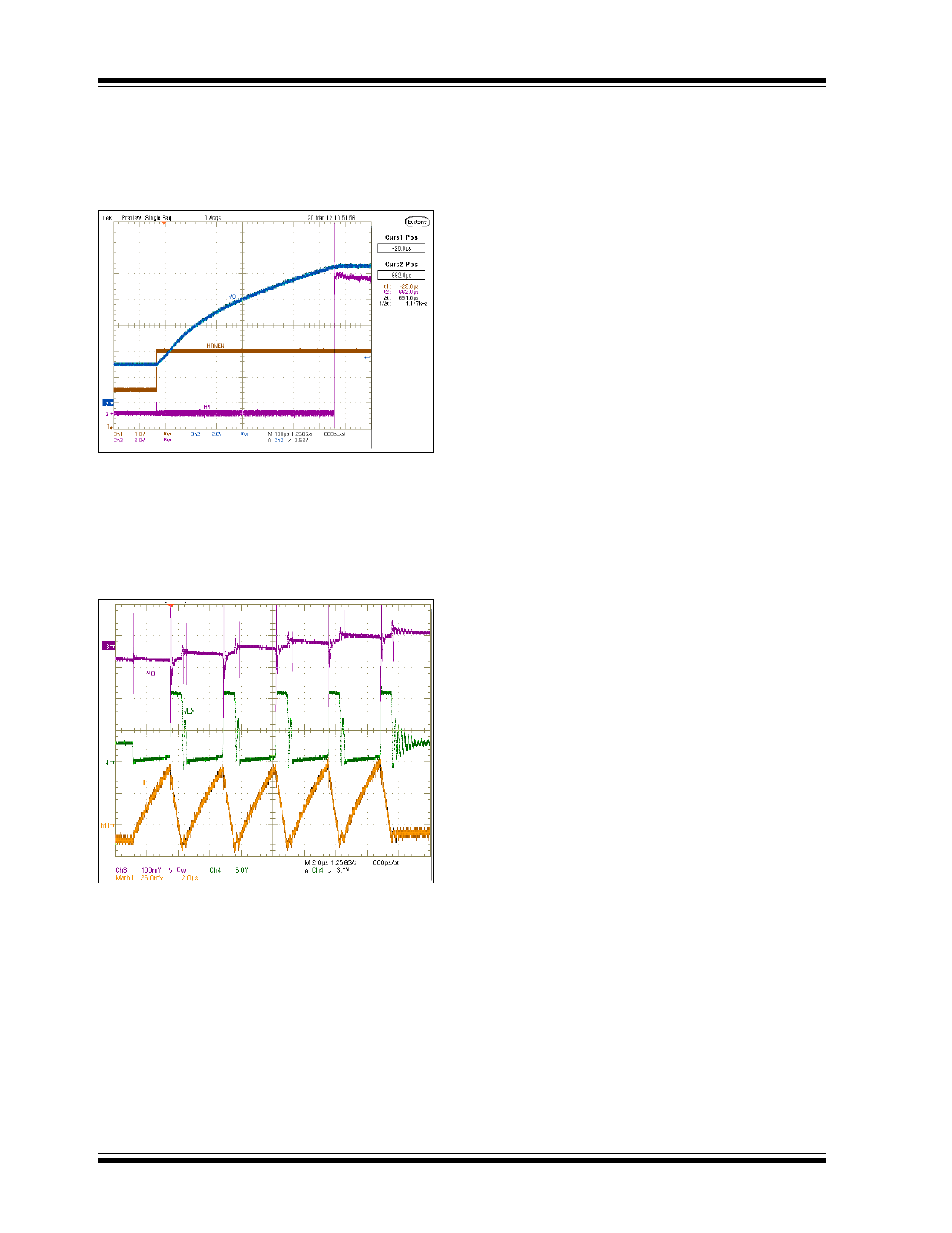
Figure 3-1
shows the horn turn-on delay after the
HRNEN has been asserted high. After the boost
voltage reaches its nominal set point, the HORNB
output turns on. In this case, the HORNB output is
driving a load current of 20 mA DC.
FIGURE 3-1:
RE46C317 Horn Turn-On
Delay.
Figure 3-2
shows the typical switching waveforms of
the boost regulator. The top waveform shows the boost
output, the center waveform shows the LX switching
waveform, and the lower waveform shows the inductor
current.
FIGURE 3-2:
RE46C317/18 Switching
Waveforms.