
2013 Microchip Technology Inc.
DS25163A-page 1
RE46C311/2
Features
• Low Quiescent Current: 600 nA/Amplifier (typical)
• Rail-to-Rail Input/Output
• Gain Bandwidth Product: 10 kHz (typical)
• Wide Supply Voltage Range: 1.8V to 5.5V
• Unity Gain Stable
• Available in Single and Dual Configurations
• Temperature Ranges: -10°C to +60°C
Applications
• Ionization Smoke Detectors
• Low Leakage High-Impedance Input Circuits
• Battery-Powered Circuits
Design Aids
• MAPS (Microchip Advanced Part Selector)
• Analog Demonstration and Evaluation Boards
• Application Notes
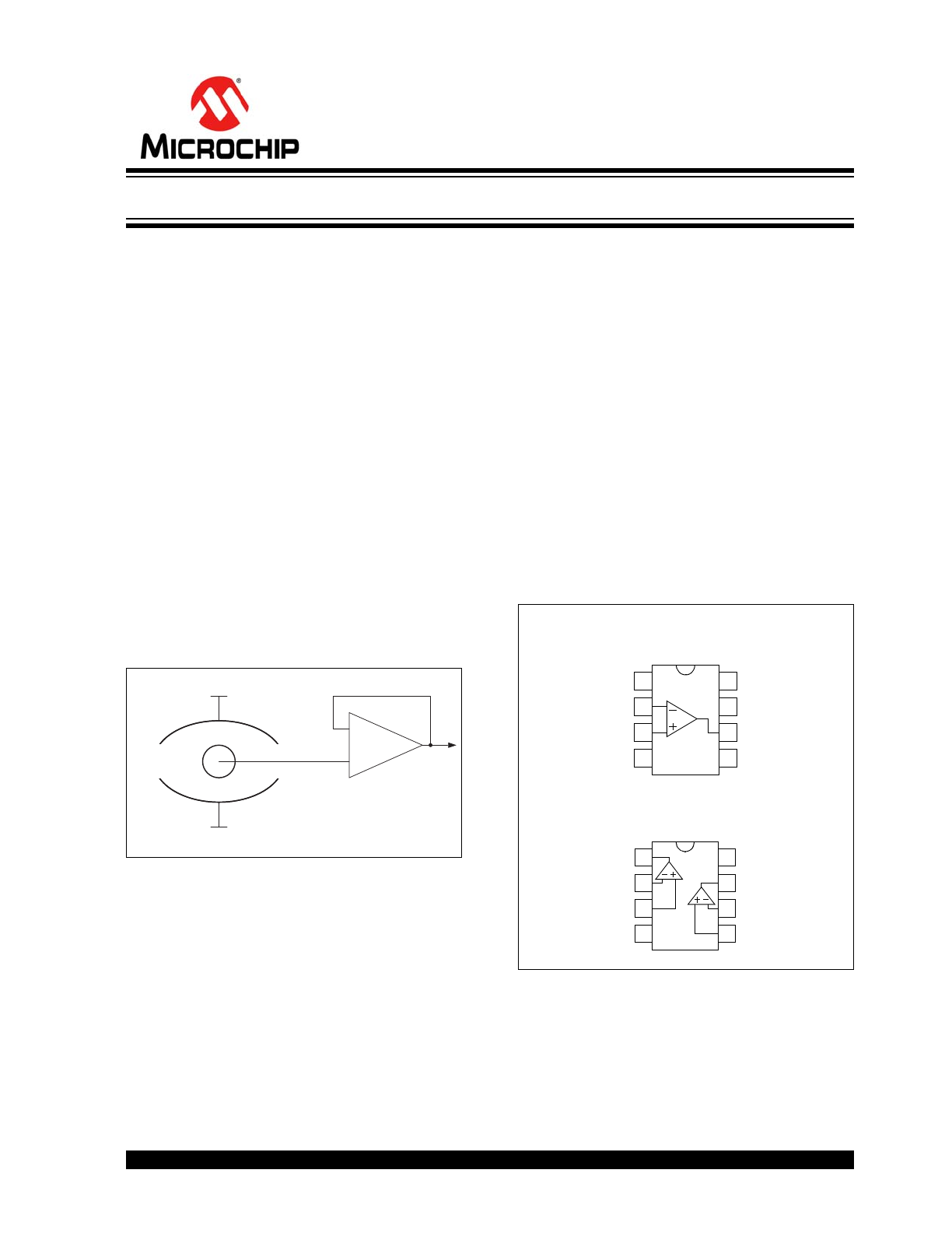
Typical Application
Description
The RE46C311/2 family of operational amplifiers (op
amps) from Microchip Technology Inc. operate with a
single-supply voltage as low as 1.8V, while drawing
less than 1 µA (maximum) of quiescent current per
amplifier. These devices are also designed to support
rail-to-rail input and output operation. This combination
of features supports battery-powered and portable
applications.
The RE46C311/2 amplifiers have a gain-bandwidth
product of 10 kHz (typical) and are unity gain stable.
These specifications make these op amps appropriate
for low-frequency applications, such as ionization
smoke detectors and sensor conditioning.
The RE46C311/2 family operational amplifiers are
offered in single (RE46C311), and dual (RE46C312)
configurations.
Package Types
+
-
VDD
VSS
Ionization
Chamber
RE46C31X
V
IN
+
V
IN
–
V
SS
V
DD
V
OUT
1
2
3
4
8
7
6
5 NC
NC
NC
V
INA
+
V
INA
–
V
SS
V
OUTB
V
INB
–
1
2
3
4
8
7
6
5 V
INB
+
V
DD
V
OUTA
RE46C311
PDIP, SOIC
RE46C312
PDIP, SOIC
Low-Input Leakage, Rail-to-Rail Input/Output Op Amps
RE46C311/2
DS25163A-page 2
2013 Microchip Technology Inc.
1.0
ELECTRICAL
CHARACTERISTICS
Absolute Maximum Ratings †
V
DD
– V
SS
........................................................................6.0V
Current at Input Pins .....................................................±2 mA
All Inputs and Outputs .................... V
SS
– 0.3V to V
DD
+ 0.3V
Difference Input voltage ...................................... |V
DD
– V
SS
|
Output Short Circuit Current ..................................continuous
Current at Output and Supply Pins ............................±30 mA
Storage Temperature.................................... –65°C to +150°C
Junction Temperature.................................................. +150°C
ESD protection on all pins (HBM; MM)
4 kV; 400V
† Notice: Stresses above those listed under “Absolute
Maximum Ratings” may cause permanent damage to
the device. This is a stress rating only and functional
operation of the device at those or any other conditions
above those indicated in the operational listings of this
specification is not implied. Exposure to maximum rat-
ing conditions for extended periods may affect device
reliability.
†† See
Section 4.1, Rail-to-Rail Input
.
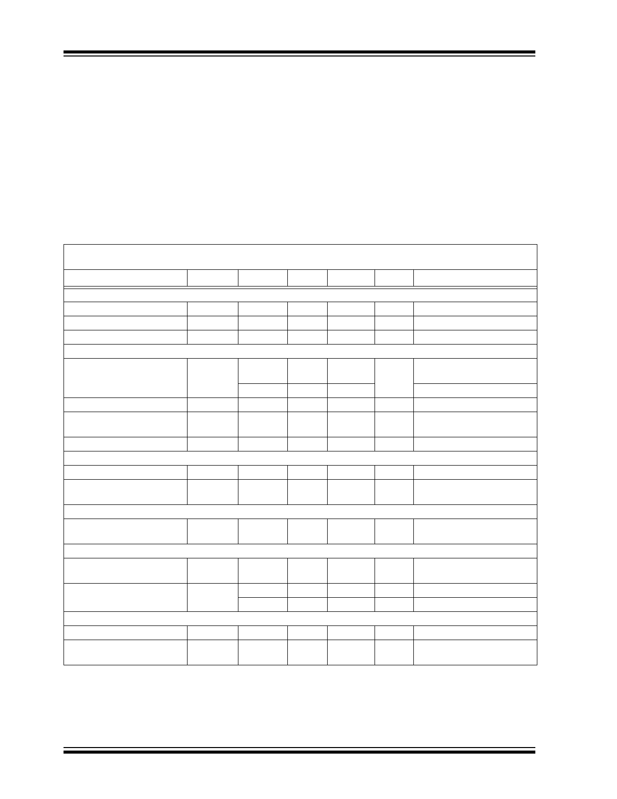
DC ELECTRICAL CHARACTERISTICS
Electrical Characteristics: Unless otherwise indicated, V
DD
= +1.8V to +5.5V, V
SS
= GND, T
A
= +25°C,
V
CM
= V
DD
/2, V
OUT
V
DD
/2, V
L
= V
DD
/2, and R
L
= 1 M
to V
L
(refer to
Figure 1-1
and
Figure 1-2
).
Parameters
Sym.
Min.
Typ.
Max.
Units
Conditions
Input Offset
Input Offset Voltage
V
OS
-3
—
+3
mV
Drift with Temperature
V
OS
/
T
A
—
±2
—
µV/°C
T
A
= -10°C to +60°C
Power Supply Rejection
PSRR
70
76
—
dB
V
CM
= V
SS
Input Leakage Current and Impedance
Input Leakage Current
I
L1
-0.75
—
0.75
pA
Non Inverting Input only,
V
IN
= V
DD
or V
SS
—
3.5
6
T
A
= +60°C
Input Leakage Current
I
L2
-100
—
100
nA
Inverting input only
Common Mode
Input Impedance
Z
CM
—
10
13
||6
—
||pF
Differential Input Impedance
Z
DIFF
—
10
13
||6
—
||pF
Common Mode
Common-Mode Input Range
V
CMR
V
SS
—
V
DD
V
Common-Mode
Rejection Ratio
CMRR
62
86
—
dB
V
DD
= 5V, V
CM
= 0V to 5.0V
Open-Loop Gain
DC Open-Loop Gain
(large signal)
A
OL
85
115
—
dB
R
L
= 50 k
to V
L
,
V
OUT
= 0.1V to V
DD
-0.1V
Output
Maximum Output
Voltage Swing
V
OL
, V
OH
V
SS
+ 10
—
V
DD
- 10
mV
R
L
= 50 k
to V
L
,
0.5V input overdrive
Output Short Circuit Current
I
SC
—
5
—
mA
V
DD
= 1.8V
—
27
—
mA
V
DD
= 5.5V
Power Supply
Supply Voltage
V
DD
1.8
—
5.5
V
Quiescent Current
per Amplifier
I
Q
0.3
0.6
1.0
µA
I
O
= 0
2013 Microchip Technology Inc.
DS25163A-page 3
RE46C311/2
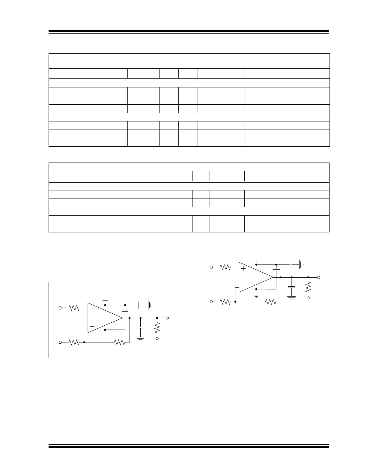
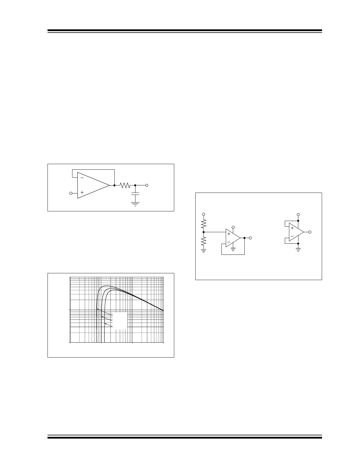
1.1
Test Circuits
The test circuits used for the DC and AC tests are
shown in
Figure 1-1
and
Figure 1-2
. The bypass
capacitors are laid out according to the rules discussed
in
Section 4.5, Supply Bypass
.
FIGURE 1-1:
AC and DC Test Circuit for
Most Non-Inverting Gain Conditions.
FIGURE 1-2:
AC and DC Test Circuit for
Most Inverting Gain Conditions.
AC ELECTRICAL CHARACTERISTICS
Electrical Characteristics: Unless otherwise indicated, V
DD
= +1.8V to +5.5V, V
SS
= GND, T
A
= +25°C,
V
CM
= V
DD
/2, V
OUT
V
DD
/2, V
L
= V
DD
/2, R
L
= 1 M
to V
L
, and C
L
= 60 pF (refer to
Figure 1-1
and
Figure 1-2
).
Parameters
Sym.
Min.
Typ.
Max.
Units
Conditions
AC Response
Gain Bandwidth Product
GBWP
—
10
—
kHz
Slew Rate
SR
—
3.0
—
V/ms
Phase Margin
PM
—
65
—
°
G = +1 V/V
Noise
Input Voltage Noise
E
ni
—
5.0
—
µV
P-P
f = 0.1 Hz to 10 Hz
Input Voltage Noise Density
e
ni
—
170
—
nV/
Hz f = 1 kHz
Input Current Noise Density
i
ni
—
0.6
—
fA/
Hz
f = 1 kHz
TEMPERATURE CHARACTERISTICS
Electrical Characteristics: Unless otherwise indicated, V
DD
= +1.8V to +5.5V, V
SS
= GND.
Parameters
Sym.
Min.
Typ.
Max. Units
Conditions
Temperature Ranges
Operating Temperature Range
T
A
-10
—
+60
°C
Storage Temperature Range
T
A
-65
—
+150
°C
Thermal Package Resistances
Thermal Resistance, 8L-PDIP
JA
—
89.3
—
°C/W
Thermal Resistance, 8L-SOIC
JA
—
149.5
—
°C/W
V
DD
R
G
R
F
R
N
V
OUT
V
IN
V
DD
/2
1 µF
C
L
R
L
V
L
0.1 µF
RE46C31X
V
DD
R
G
R
F
R
N
V
OUT
V
DD
/2
V
IN
1 µF
C
L
R
L
V
L
0.1 µF
RE46C31X
RE46C311/2
DS25163A-page 4
2013 Microchip Technology Inc.
2.0
TYPICAL PERFORMANCE CURVES
Note: Unless otherwise indicated, T
A
= +25°C, V
DD
= +1.8V to +5.5V, V
SS
= GND, V
CM
= V
DD
/2, V
OUT
V
DD
/2,
V
L
= V
DD
/2, R
L
= 1 M
to V
L
, and C
L
= 60 pF.
FIGURE 2-1:
Input Offset Voltage vs.
Common Mode Input Voltage with V
DD
= 1.8V.
FIGURE 2-2:
Input Offset Voltage vs.
Common Mode Input Voltage with V
DD
= 5.5V.
FIGURE 2-3:
CMRR, PSRR vs.
Frequency.
FIGURE 2-4:
The RE46C311/2 Family
Shows No Phase Reversal.
FIGURE 2-5:
CMRR, PSRR vs. Ambient
Temperature.
FIGURE 2-6:
Open-Loop Gain, Phase vs.
Frequency.
Note:
The graphs and tables provided following this note are a statistical summary based on a limited number of
samples and are provided for informational purposes only. The performance characteristics listed herein
are not tested or guaranteed. In some graphs or tables, the data presented may be outside the specified
operating range (e.g., outside specified power supply range) and therefore outside the warranted range.
-2000
-1500
-1000
-500
0
500
1000
1500
2000
-0.4-0.2 0 0.2 0.4 0.6 0.8 1 1.2 1.4 1.6 1.8 2 2.2
Input Offset V
o
ltage (μV)
Common Mode Input Voltage (V)
T
A
= +60°C
T
A
= +25°C
T
A
= -10°C
V
DD
=
V
Representative Part
-2000
-1500
-1000
-500
0
500
1000
1500
2000
-0.5 0 0.5 1 1.5 2 2.5 3 3.5 4 4.5 5 5.5 6
Input Offset V
o
ltage
(μV)
Common Mode Input Voltage (V)
V
DD
= 5.5V
Representative Part
T
A
= +60°C
T
A
= +25°C
T
A
= -10°C
20
30
40
50
60
70
80
90
1
10
100
1000
CMRR, PSRR
(dB)
Frequency (Hz)
CMRR
PSRR-/+
-1
0
1
2
3
4
5
6
Input, Output V
o
ltages
(V)
Time (5 ms/div)
G = 2 V/V
V
DD
= 5V
Input
Output
70
75
80
85
90
95
100
-10
0
10
20
30
40
50
60
PSRR, CMRR (dB)
Ambient Temperature (°C)
PSRR
CMRR
(V
DD
=5.5V, V
CM
= -0.3V to +5.8V)
-210
-180
-150
-120
-90
-60
-30
0
-20
0
20
40
60
80
100
120
1.0E-03
1.0E-02
1.0E-01
1.0E+00
1.0E+01
1.0E+02
1.0E+03
1.0E+04
1.0E+05
Open-Loop Phase
(°)
Open-Loop Gain (dB)
Frequency (Hz)
Open-Loop Gain
Open-Loop Phase
0.001 0.01 0.1 1 10 100 1k 10k 100k
2013 Microchip Technology Inc.
DS25163A-page 5
RE46C311/2
Note: Unless otherwise indicated, T
A
= +25°C, V
DD
= +1.8V to +5.5V, V
SS
= GND, V
CM
= V
DD
/2, V
OUT
V
DD
/2,
V
L
= V
DD
/2, R
L
= 1 M
to V
L
, and C
L
= 60 pF.
FIGURE 2-7:
DC Open-Loop Gain vs.
Power Supply Voltage.
FIGURE 2-8:
Gain Bandwidth Product,
Phase Margin vs. Common Mode Input Voltage.
FIGURE 2-9:
Gain Bandwidth Product,
Phase Margin vs. Ambient Temperature with
V
DD
= 5.5V.
FIGURE 2-10:
Small Signal Non-inverting
Pulse Response.
FIGURE 2-11:
Small Signal Inverting Pulse
Response.
FIGURE 2-12:
Large Signal Non-inverting
Pulse Response.
80
90
100
110
120
130
140
1.5
2.0
2.5
3.0
3.5
4.0
4.5
5.0
5.5
6.0
DC Open-Loop Gain (dB)
Power Supply Voltage (V)
R
L
= 50 k
V
OUT
= 0.1V to V
DD
– 0.1V
0
10
20
30
40
50
60
70
80
90
100
0
2
4
6
8
10
12
14
16
18
20
-0.500.00 0.50 1.00 1.50 2.00 2.50 3.00 3.50 4.00 4.50 5.00 5.50
Phase Mar
g
in (°)
GBWP
(kHz)
Common Mode Voltage (V)
PM
GBWP
V
DD
= 5.5V
Gain = 100
20
30
40
50
60
70
80
90
0
2
4
6
8
10
12
14
-10
0
10
20
30
40
50
60
Phase Mar
g
in (°)
Gain Bandw
idth Product
(KHz)
Ambient Temperature (°C)
GBWP
PM
V
DD
= 5.5V
Output V
o
ltage
(5 mV/div)
Time (100 μs/div)
G = 1 V/V
R
L
= 50 k
Ω
Ω
Output V
o
ltage
(5 mV/div)
Time (100 μs/div)
G = -1 V/V
R
L
= 50 k
Ω
Ω
0.0
0.5
1.0
1.5
2.0
2.5
3.0
3.5
4.0
4.5
5.0
Output V
o
ltage
(V)
Time (1 ms/div)
G = -1 V/V
R
L
= 50 k
Ω
V
DD
= 5.0V
RE46C311/2
DS25163A-page 6
2013 Microchip Technology Inc.
Note: Unless otherwise indicated, T
A
= +25°C, V
DD
= +1.8V to +5.5V, V
SS
= GND, V
CM
= V
DD
/2, V
OUT
V
DD
/2,
V
L
= V
DD
/2, R
L
= 1 M
to V
L
, and C
L
= 60 pF.
FIGURE 2-13:
Large Signal Inverting Pulse
Response.
0.0
0.5
1.0
1.5
2.0
2.5
3.0
3.5
4.0
4.5
5.0
Output V
o
ltage
(V)
Time (1 ms/div)
G = 1 V/V
R
L
= 50 k
Ω
V
DD
= 5.0V
2013 Microchip Technology Inc.
DS25163A-page 7
RE46C311/2
3.0
PIN DESCRIPTIONS
Descriptions of the pins are listed in
Table 3-1
.
3.1
Analog Outputs
The output pins are low-impedance voltage sources.
3.2
Analog Inputs
The non-inverting and inverting inputs are high-imped-
ance CMOS inputs with low bias and leakage currents.
3.3
Power Supply Pins
The positive power supply pin (V
DD
) is 1.8V to 5.5V
higher than the negative power supply pin (V
SS
). For
normal operation, the other pins are at voltages
between V
SS
and V
DD
.
Typically, these parts are used in a single (positive)
supply configuration. In this case, V
SS
is connected to
ground and V
DD
is connected to the supply. V
DD
will
need bypass capacitors.
TABLE 3-1:
PIN FUNCTION TABLE
RE46C311
RE46C312
Symbol
Description
PDIP, SOIC
PDIP, SOIC,
6
1
V
OUT
, V
OUTA
Analog Output (op amp A)
2
2
V
IN
–, V
INA
–
Inverting Input (op amp A)
3
3
V
IN
+, V
INA
+
Non-inverting Input (op amp A)
7
8
V
DD
Positive Power Supply
—
5
V
INB
+
Non-inverting Input (op amp B)
—
6
V
INB
–
Inverting Input (op amp B)
—
7
V
OUTB
Analog Output (op amp B)
4
4
V
SS
Negative Power Supply
1, 5, 8
—
NC
No Internal Connection
RE46C311/2
DS25163A-page 8
2013 Microchip Technology Inc.
4.0
APPLICATIONS INFORMATION
The RE46C311/2 family of op amps is manufactured
using a state of the art CMOS process. These op amps
are unity gain stable and suitable for a wide range of
general purpose, low-power applications.
4.1
Rail-to-Rail Input
4.1.1
PHASE REVERSAL
The RE46C311/2 op amps are designed to not exhibit
phase inversion when the input pins exceed the supply
voltages.
Figure 2-4
shows an input voltage exceeding
both supplies with no phase inversion.
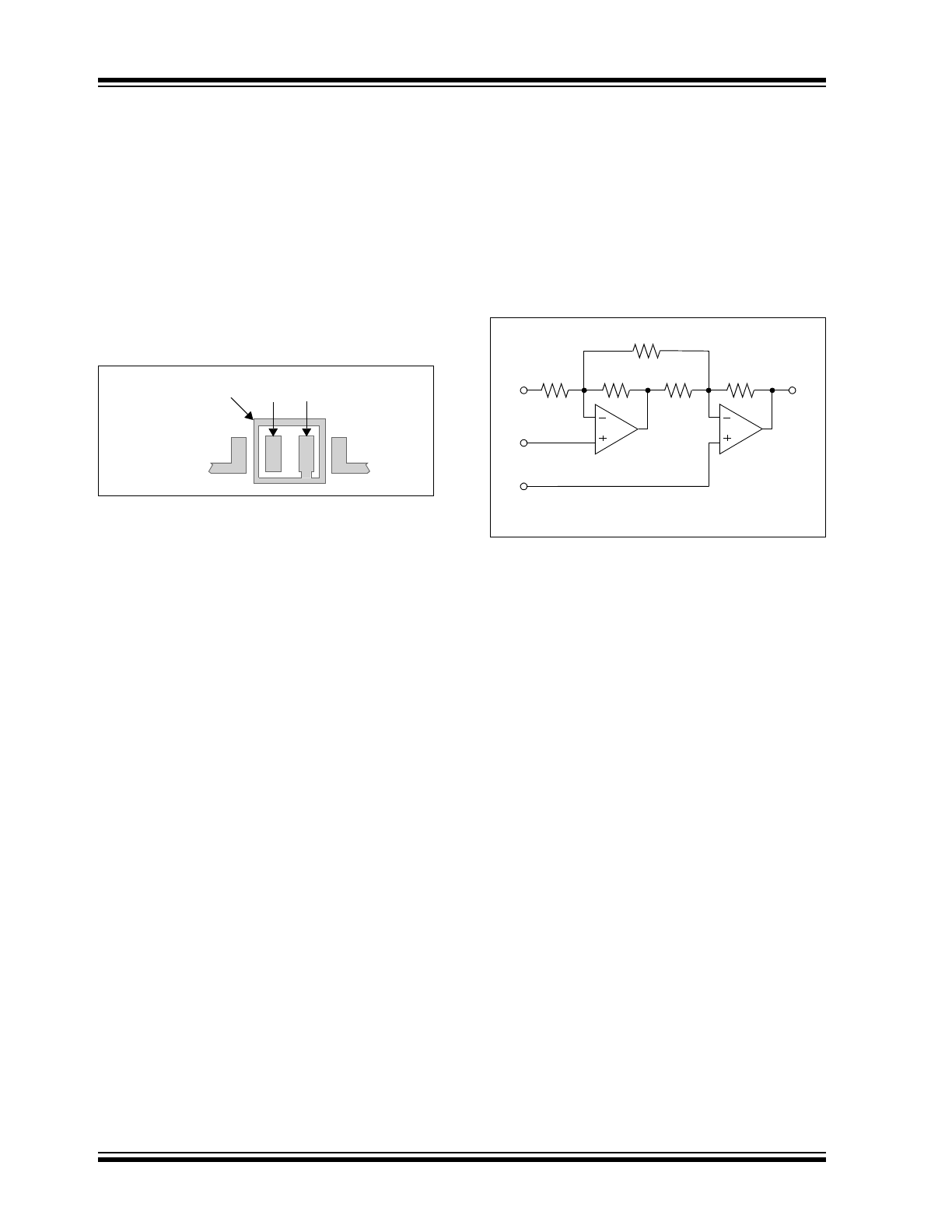
4.1.2
INPUT VOLTAGE AND CURRENT
LIMITS
The ESD protection on the inputs can be depicted as
shown in
Figure 4-1
. This structure was chosen to
protect the input transistors and to minimize input bias
current (I
B
). The input ESD diodes clamp the inputs
when they try to go more than one diode drop below
V
SS
or one diode drop above V
DD
.
FIGURE 4-1:
Simplified Analog Input ESD
Structures.
In order to prevent damage and/or improper operation
of these amplifiers, the circuit must limit the currents
(and voltages) at the input pins (see
Absolute
Maximum Ratings †
).
A significant amount of current can flow out of the
inputs (through the ESD diodes) when the common
mode voltage (V
CM
) is below V
SS
or above V
DD
.
Applications that are high-impedance may need to limit
the usable voltage range.
4.1.3
NORMAL OPERATION
The input stage of the RE46C311/2 op amps uses two
differential input stages in parallel. One operates at a
low common mode input voltage (V
CM
), while the other
operates at a high V
CM
. With this topology, the device
operates with a V
CM
up to V
DD
and down to V
SS
. The
input offset voltage is measured at V
CM
= V
SS
and V
DD
to ensure proper operation.
There are two transitions in input behavior as V
CM
is
changed. The first occurs when V
CM
is near
V
SS
+ 0.4V, and the second occurs when V
CM
is near
V
DD
– 0.5V (see
Figure 2-1
and
Figure 2-2
). For the
best distortion performance with non-inverting gains,
avoid these regions of operation.
4.2
Rail-to-Rail Output
There are two specifications that describe the output
swing capability of the RE46C311/2 family of op amps.
The first specification (Maximum Output Voltage
Swing) defines the absolute maximum swing that can
be achieved under the specified load condition. Thus,
the output voltage swings to within 10 mV of either
supply rail with a 50 k
load to V
DD
/2.
Figure 2-4
shows how the output voltage is limited when the input
goes beyond the linear region of operation.
The second specification that describes the output
swing capability of these amplifiers is the Linear Output
Voltage Range. This specification defines the maxi-
mum output swing that can be achieved while the
amplifier still operates in its linear region. To verify
linear operation in this range, the large signal DC
Open-Loop Gain (A
OL
) is measured at points inside the
supply rails. The measurement must meet the specified
A
OL
condition in the specification table.
4.3
Output Loads and Battery Life
The RE46C311/2 op amp family has outstanding
quiescent current, which supports battery-powered
applications.
Heavy resistive loads at the output can cause
excessive battery drain. Driving a DC voltage of 2.5V
across a 100 k
load resistor will cause the supply
current to increase by 25 µA, depleting the battery
43 times as fast as I
Q
(0.6 µA, typical) alone.
High frequency signals (fast edge rate) across
capacitive loads will also significantly increase supply
current. For instance, a 0.1 µF capacitor at the output
presents an AC impedance of 15.9 k
(1/2fC) to a
100 Hz sine wave. It can be shown that the average
power drawn from the battery by a 5.0 V
p-p
sine wave
(1.77 V
rms
), under these conditions, is:
EQUATION 4-1:
This will drain the battery 17 times as fast as I
Q
alone.
Bond
Pad
Bond
Pad
Bond
Pad
V
DD
V
IN
+
V
SS
Input
Stage
Bond
Pad
V
IN
–
P
Supply
= (V
DD
- V
SS
) (I
Q
+ V
L(p-p)
f
C
L
)
= (5V)(0.6 µA + 5.0V
p-p
·
100Hz
·
0.1µF)
= 3.0 µW + 50 µW
2013 Microchip Technology Inc.
DS25163A-page 9
RE46C311/2
4.4
Capacitive Loads
Driving large capacitive loads can cause stability
problems for voltage feedback op amps. As the load
capacitance increases, the feedback loop’s phase
margin decreases and the closed-loop bandwidth is
reduced. This produces gain peaking in the frequency
response, with overshoot and ringing in the step
response. A unity gain buffer (G = +1) is the most
sensitive to capacitive loads, although all gains show
the same general behavior.
When driving large capacitive loads with these op
amps (e.g., > 60 pF when G = +1), a small series
resistor at the output (R
ISO
in
Figure 4-2
) improves the
feedback loop’s phase margin (stability) by making the
output load resistive at higher frequencies. The
bandwidth will be generally lower than the bandwidth
with no capacitive load.
FIGURE 4-2:
Output Resistor, R
ISO
,
Stabilizes Large Capacitive Loads.
Figure 4-3
gives recommended R
ISO
values for
different capacitive loads and gains. The x-axis is the
normalized load capacitance (C
L
/G
N
), where G
N
is the
circuit’s noise gain. For non-inverting gains, G
N
and the
Signal Gain are equal. For inverting gains, G
N
is
1+|Signal Gain| (e.g., -1 V/V gives G
N
= +2 V/V).
FIGURE 4-3:
Recommended R
ISO
Values
for Capacitive Loads.
After selecting R
ISO
for your circuit, double check the
resulting frequency response peaking and step
response overshoot. Modify R
ISO
’s value until the
response is reasonable.
4.5
Supply Bypass
With this family of operational amplifiers, the power
supply pin (V
DD
for single supply) should have a local
bypass capacitor (i.e., 0.01 µF to 0.1 µF) within 2 mm
for good high-frequency performance. It can use a bulk
capacitor (i.e., 1 µF or larger) within 100 mm to provide
large, slow currents. This bulk capacitor is not required
for most applications and can be shared with nearby
analog parts.
4.6
Unused Op Amps
An unused op amp in a dual package (RE46C312)
should be configured as shown in
Figure 4-4
. These
circuits prevent the output from toggling and causing
crosstalk. Circuit A sets the op amp at its minimum
noise gain. The resistor divider produces any desired
reference voltage within the output voltage range of the
op amp; the op amp buffers that reference voltage.
Circuit B uses the minimum number of components
and operates as a comparator, but it may draw more
current.
FIGURE 4-4:
Unused Op Amps.
V
IN
R
ISO
V
OUT
C
L
RE46C31X
1,000
10,000
100,000
1.E+01
1.E+02
1.E+03
1.E+04
Recommended R
ISO
(ȍ
)
Normalized Load Capacitance; C
L
/G
N
(F)
10p
1k
100k
100p
G
N
= +1
G
N
= +2
G
N
≥ +5
10k
10n
1n
V
DD
V
DD
R
1
R
2
V
DD
V
REF
V
R EF
V
DD
R
2
R
1
R
2
+
-------------------
=
½ RE46C312 (A)
½ RE46C312 (B)
RE46C311/2
DS25163A-page 10
2013 Microchip Technology Inc.
4.7
PCB Surface Leakage
In applications where low input bias current is critical,
printed circuit board (PCB) surface leakage effects
need to be considered. Surface leakage is caused by
humidity, dust or other contamination on the board.
Under low humidity conditions, a typical resistance
between nearby traces is 10
12
. A 5V difference would
cause 5 pA of current to flow, which is greater than the
RE46C311/2 family’s leakage current at +25°C.
The easiest way to reduce surface leakage is to use a
guard ring around sensitive pins (or traces). The guard
ring is biased at the same voltage as the sensitive pin.
Figure 4-5
shows an example of this type of layout.
FIGURE 4-5:
Example Guard Ring Layout
for Inverting Gain.
1.
Non-inverting Gain and Unity Gain Buffer:
a)
Connect the non-inverting pin (V
IN
+) to the
input with a wire that does not touch the
PCB surface.
b)
Connect the guard ring to the inverting input
pin (V
IN
–). This biases the guard ring to the
Common mode input voltage.
2.
Inverting Gain and Transimpedance Gain
(convert current to voltage, such as photo
detectors) amplifiers:
a)
Connect the guard ring to the non-inverting
input pin (V
IN
+). This biases the guard ring
to the same reference voltage as the op
amp (e.g., V
DD
/2 or ground).
b)
Connect the inverting pin (V
IN
–) to the input
with a wire that does not touch the PCB
surface.
4.8
Application Circuits
4.8.1
INSTRUMENTATION AMPLIFIER
The RE46C311/2 op amp is well suited for conditioning
sensor signals in battery-powered applications.
Figure 4-6
shows a two op amp instrumentation
amplifier, using the RE46C312, that works well for
applications requiring rejection of Common mode noise
at higher gains. The reference voltage (V
REF
) is
supplied by a low impedance source. In single supply
applications, V
REF
is typically V
DD
/2.
.
FIGURE 4-6:
Two Op Amp
Instrumentation Amplifier.
Guard Ring
V
IN
– V
IN
+
V
OUT
V
1
V
2
–
1
R
1
R
2
------
2R
1
R
G
---------
+
+
V
REF
+
=
V
REF
R
1
R
2
R
2
R
1
V
OUT
R
G
V
2
V
1
½
RE46C312
½
RE46C312