
2013-2017 Microchip Technology Inc.
DS20005225E-page 1
RE46C191
Features:
• Two AA Battery Operation
• Low Quiescent Current Consumption
• Local Alarm Memory
• Interconnect up to 40 Detectors
• Nine-Minute Timer for Sensitivity Control
• Temporal or Continuous Horn Pattern
• Internal Low Battery and Chamber Test
• All-Internal Oscillator
• Internal Infrared Emitter Diode (IRED) Driver
• Adjustable IRED Drive Current
• Adjustable Hush Sensitivity
• Two percent Low Battery Set Point
• Pin-for-Pin Compatible with RE46C190
General Description:
The RE46C191 is a low-power, low-voltage CMOS
photoelectric-type smoke detector IC. With minimal
external components, this circuit provides all the
required features for a photoelectric-type smoke
detector.
The design incorporates a gain-selectable photo
amplifier for use with an infrared emitter/detector pair.
To keep the standby current to a minimum, an internal
oscillator strobes power to the smoke detection
circuitry every 10 seconds. If smoke is sensed, the
detection rate is increased to verify an Alarm condition.
A High Gain mode is available for push button chamber
testing.
A check for a Low Battery condition is performed every
86 seconds, and the chamber integrity is tested once
every 43 seconds when in Standby. The temporal horn
pattern supports the NFPA 72 emergency evacuation
signal.
An interconnect pin allows multiple detectors to be
connected such that, when one unit alarms, all units will
sound.
An internal nine-minute timer can be used for a
Reduced Sensitivity mode.
Utilizing low-power CMOS technology, the RE46C191
is designed for use in smoke detectors that comply with
Underwriters Laboratory Specification UL217.
PIN CONFIGURATION
RE46C191
SOIC
V
SS
1
2
3
4
5
6
7
8
16
15
14
13
12
11
10
9
IRED
V
DD
TEST
TEST2
IRP
IRN
RLED
LX
V
BST
HS
HB
IO
IRCAP
FEED
GLED
CMOS Low-Voltage Photoelectric Smoke Detector ASIC
with Interconnect and Timer Mode
RE46C191
DS20005225E-page 2
2013-2017 Microchip Technology Inc.
TYPICAL BLOCK DIAGRAM
Control
Logic and
Timing
Trimmed
Oscilator
POR and
BIAS
+
-
+
-
V
DD
(3)
IRCAP (11)
IRN (7)
IRED (2)
TEST (4)
R4
R3
LX (16)
FEED (10)
HS (14)
V
BST
(15)
RLED (8)
GLED (9)
HB (13)
IRP (6)
V
SS
(1)
Interconnect
+
-
Programmable
IRED Current
Programmable
Limits
Photo
Integrator
Precision
Reference
+
-
TEST2 (5)
Horn Driver
Level
Shift
IO (12)
Current
Sense
Boost Control
Boost Comparator
Low Battery
Comparator
Smoke
Comparator
Programming
Control
High
Normal
Hysteresis
2013-2017 Microchip Technology Inc.
DS20005225E-page 3
RE46C191
TYPICAL BATTERY APPLICATION
Note 1:
C2 should be located as close as possible to the device power pins. C1 should be located closest to V
SS
.
2:
R3, R4, and C5 are typical values and may be adjusted to maximize sound pressure.
3:
DC-DC converter in High Boost mode (nominal V
BST
= 9.6V) can draw current pulses of greater than 1A
and is very sensitive to series resistance. Critical components of this resistance are the inductor DC
resistance, the internal resistance of the battery, and the resistance in the connections from the inductor to
the battery, from the inductor to the LX pin and from the V
SS
pin to the battery. To function properly under
full load at V
DD
= 2V, the total of the inductor and interconnect resistances should not exceed 0.3
. The
internal battery resistance should not be more than 0.5
and a low ESR capacitor of 10 µF or more should
be connected in parallel with the battery to average the current draw over the boost converter cycle.
4:
Schottky diode D1 must have a maximum peak current rating of at least 1.5A. For best results, it should
have a forward voltage specification of less than 0.5V at 1A and low reverse leakage.
5:
Inductor L1 must have a maximum peak current rating of at least 1.5A.
16
15
14
13
12
11
10
9
8
7
6
5
3
2
1
V
SS
IRED
V
DD
TEST
TEST2
IRP
IRN
RLED
FEED
GLED
IRCAP
IO
HB
HS
V
BST
LX
RE46C191
D2
D3
4
9
D1
4.7 µF
C4
200K
R3
1.5M
R4
1 nF
C5
L1
10 µH
330
R5
33 µF
C6
To other Units
1 µF
C2
100
R1
10 µF
C1
V
DD
Push-to-Test/
Hush
V
BST
330
R6
100
R7
D4
RED
D5
GREEN
C3
Smoke
Chamber
Battery
3V
TP1
TP2
V
BST
100 µF
RE46C191
DS20005225E-page 4
2013-2017 Microchip Technology Inc.
1.0
ELECTRICAL
CHARACTERISTICS
Absolute Maximum Ratings†
Supply Voltage ..................................V
DD
= 5.5V; V
BST
= 13V
Input Voltage Range Except
FEED and TEST ................................... V
IN
= -0.3V to V
DD
+ 0.3V
FEED Input Voltage Range .................... V
INFD
= -10 to +22V
TEST Input Voltage Range .. V
INTEST
= -0.3V to V
BST
+ 0.3V
LX Voltage................................................ V
LX
= -0.3V to 13V
Maximum IRCAP
Voltage................................ V
IRCAP
= 5.5V
Input Current except FEED ...................................I
IN
= 10 mA
Continuous Operating Current
(HS, HB, and V
BST
) ........................................... I
O
= 40 mA
Continuous Operating Current (IRED) ............. I
OIR
= 300 mA
Operating Temperature ...............................T
A
= -10 to +60°C
Storage Temperature............................ T
STG
= -55 to +125°C
ESD Human Body Model .................................... V
HBM
= 2 kV
ESD Machine Model ........................................... V
MM
= 175V
† Notice:
Stresses above those listed under “Maximum
ratings” may cause permanent damage to the device.
This is a stress rating only, and the functional operation
of the device at these or any other conditions above
those indicated in the operation listings of this
specification is not implied. Exposure to maximum
rating conditions for extended periods may affect
device reliability.
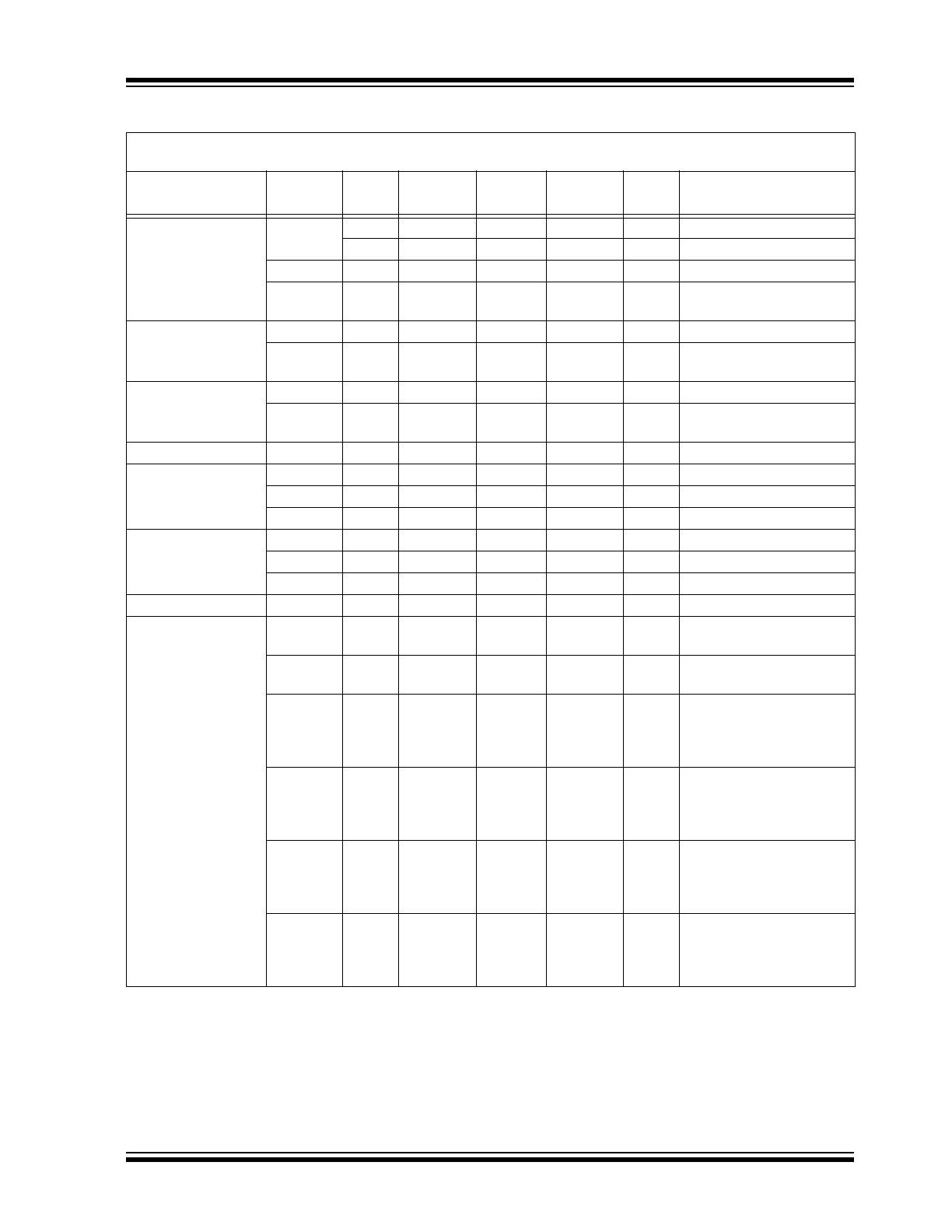
DC ELECTRICAL CHARACTERISTICS
DC Electrical Characteristics:
Unless otherwise indicated, all parameters apply at T
A
= -10 to +60°C, V
DD
= 3V,
V
BST
= 4.2V, Typical Application (unless otherwise noted) (
Note 1
,
Note 2
,
Note 3
)
Parameter
Symbol
Test
Pin
Min.
Typ.
Max.
Units
Conditions
Supply Voltage
V
DD
3
2.0
—
5.0
V
Operating
Supply Current
I
DD1
3
—
1
2
µA
Standby, Inputs low,
No loads, Boost off, No
smoke check
Standby Boost
Current
I
BST1
15
—
100
—
nA
Standby, Inputs low,
No loads, Boost off, No
smoke check
IRCAP Supply
Current
I
IRCAP
11
—
500
—
µA
During smoke check
Boost Voltage
V
BST1
15
3.0
3.6
4.2
V
IRCAP charging for smoke
check, GLED operation,
I
OUT
= 40 mA
V
BST2
15
8.5
9.6
10.7
V
No Local Alarm,
RLED Operation,
I
OUT
= 40 mA, IO as an
input
Note 1:
Wherever a specific V
BST
value is listed under test conditions, the V
BST
is forced externally with the
inductor disconnected and the DC-DC converter NOT running.
2:
Typical values are for design information only.
3:
Limits over the specified temperature range are not production tested and are based on characterization
data. Unless otherwise stated, production test is at room temperature with guardbanded limits.
4:
Not production tested
2013-2017 Microchip Technology Inc.
DS20005225E-page 5
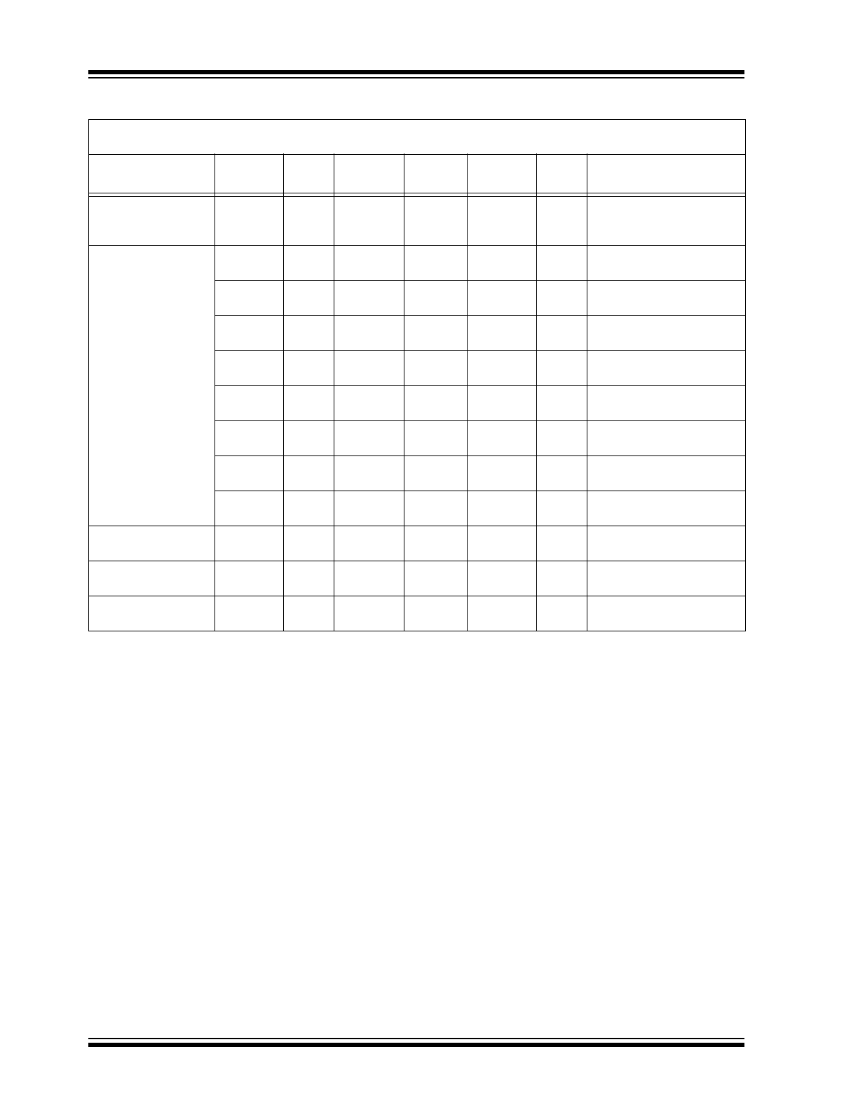
RE46C191
Input Leakage
I
INOP
6
-200
—
200
pA
IRP = V
DD
or V
SS
7
-200
—
200
pA
IRN = V
DD
or V
SS
I
IHF
10
—
20
50
µA
FEED = 22V, V
BST
= 9V
I
ILF
10
-50
-15
—
µA
FEED = -10V,
V
BST
= 10.7V
Input Voltage Low
V
IL1
10
—
—
2.7
V
FEED, V
BST
= 9V
V
IL2
12
—
—
800
mV
No Local Alarm,
IO as an input
Input Voltage High
V
IH1
10
6.2
—
—
V
FEED, V
BST
= 9V
V
IH2
12
2.0
—
—
V
No Local Alarm,
IO as an input
IO Hysteresis
V
HYST1
12
—
150
—
mV
Input Pull-Down
Current
I
PD1
4,5
3
10
30
µA
V
IN
= V
DD
I
PDIO1
12
20
—
80
µA
V
IN
= V
DD
I
PDIO2
12
—
—
140
µA
V
IN
= 15V
Output Voltage Low
V
OL1
13,14
—
—
500
mV
I
OL
= 16 mA, V
BST
= 9V
V
OL2
8
—
—
300
mV
I
OL
= 10 mA, V
BST
= 9V
V
OL3
9
—
—
300
mV
I
OL
= 10 mA, V
BST
= 3.6V
Output High Voltage
V
OH1
13,14
8.5
—
—
V
I
OL
= 16 mA, V
BST
= 9V
Output Current
I
IOH1
12
-4
-5
—
mA
Alarm, V
IO
= 3V or
V
IO
= 0V, V
BST
= 9V
I
IODMP
12
5
15
—
mA
At conclusion of Local
Alarm or Test, V
IO
= 1V
I
IRED50
2
45
50
55
mA
IRED on, V
IRED
= 1V,
V
BST
= 5V, IRCAP = 5V,
(50 mA option selected,
T
A
= 27°C)
I
IRED100
2
90
100
110
mA
IRED on, V
IRED
= 1V,
V
BST
= 5V, IRCAP = 5V,
(100 mA option selected,
T
A
= 27°C)
I
IRED150
2
135
150
165
mA
IRED on, V
IRED
= 1V,
V
BST
= 5V, IRCAP = 5V,
(150 mA option selected,
T
A
= 27°C)
I
IRED200
2
180
200
220
mA
IRED on, V
IRED
= 1V,
V
BST
= 5V, IRCAP = 5V,
(200 mA option selected,
T
A
= 27°C)
DC ELECTRICAL CHARACTERISTICS (CONTINUED)
DC Electrical Characteristics:
Unless otherwise indicated, all parameters apply at T
A
= -10 to +60°C, V
DD
= 3V,
V
BST
= 4.2V, Typical Application (unless otherwise noted) (
Note 1
,
Note 2
,
Note 3
)
Parameter
Symbol
Test
Pin
Min.
Typ.
Max.
Units
Conditions
Note 1:
Wherever a specific V
BST
value is listed under test conditions, the V
BST
is forced externally with the
inductor disconnected and the DC-DC converter NOT running.
2:
Typical values are for design information only.
3:
Limits over the specified temperature range are not production tested and are based on characterization
data. Unless otherwise stated, production test is at room temperature with guardbanded limits.
4:
Not production tested
RE46C191
DS20005225E-page 6
2013-2017 Microchip Technology Inc.
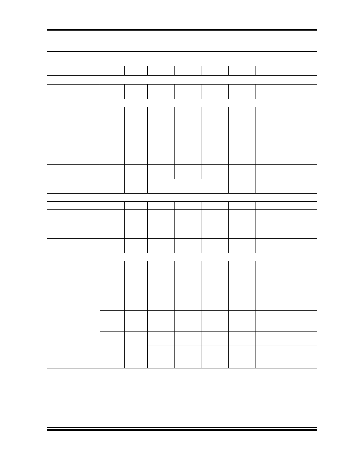
IRED Current
Temperature
Coefficient
TC
IRED
—
—
0.5
—
%/°C
V
BST
= 5V, IRCAP = 5V
(
Note 4
)
Low Battery Alarm
Voltage
V
LB1
3
2.05
2.1
2.15
V
Falling Edge,
2.1V nominal selected
V
LB2
3
2.15
2.2
2.25
V
Falling Edge,
2.2V nominal selected
V
LB3
3
2.25
2.3
2.35
V
Falling Edge,
2.3V nominal selected
V
LB4
3
2.35
2.4
2.45
V
Falling Edge,
2.4V nominal selected
V
LB5
3
2.45
2.5
2.55
V
Falling Edge,
2.5V nominal selected
V
LB6
3
2.55
2.6
2.65
V
Falling Edge,
2.6V nominal selected
V
LB7
3
2.65
2.7
2.75
V
Falling Edge,
2.7V nominal selected
V
LB8
3
2.75
2.8
2.85
V
Falling Edge,
2.8V nominal selected
Low Battery
Hysteresis
V
LBHYST
3
—
100
—
mV
IRCAP Turn-On
Voltage
V
TIR1
11
3.6
4.0
4.4
V
Falling edge,
V
BST
= 5V, I
OUT
= 20 mA
IRCAP Turn-Off
Voltage
V
TIR2
11
4.0
4.4
4.8
V
Rising edge,
V
BST
= 5V, I
OUT
= 20 mA
DC ELECTRICAL CHARACTERISTICS (CONTINUED)
DC Electrical Characteristics:
Unless otherwise indicated, all parameters apply at T
A
= -10 to +60°C, V
DD
= 3V,
V
BST
= 4.2V, Typical Application (unless otherwise noted) (
Note 1
,
Note 2
,
Note 3
)
Parameter
Symbol
Test
Pin
Min.
Typ.
Max.
Units
Conditions
Note 1:
Wherever a specific V
BST
value is listed under test conditions, the V
BST
is forced externally with the
inductor disconnected and the DC-DC converter NOT running.
2:
Typical values are for design information only.
3:
Limits over the specified temperature range are not production tested and are based on characterization
data. Unless otherwise stated, production test is at room temperature with guardbanded limits.
4:
Not production tested
2013-2017 Microchip Technology Inc.
DS20005225E-page 7
RE46C191
AC ELECTRICAL CHARACTERISTICS
AC Electrical Characteristics:
Unless otherwise indicated, all parameters apply at T
A
= -10° to +60°C, V
DD
= 3V,
V
BST
= 4.2V, Typical Application (unless otherwise noted) (
Note 1
to
Note 4
).
Parameter
Symbol Test Pin
Min.
Typ.
Max.
Units
Conditions
Time Base
Internal Clock Period
T
PCLK
—
9.80
10.4
11.0
ms
PROGSET,
IO = high
RLED Indicator
On Time
T
ON1
8
9.80
10.4
11.0
ms
Operating
Standby Period
T
PLED1
8
320
344
368
s
Standby, No alarm
Local Alarm Period
T
PLED2A
8
470
500
530
ms
Local Alarm condition
with temporal horn
pattern
T
PLED2B
8
625
667
710
ms
Local Alarm condition
with continuous horn
pattern
Hush Timer Period
T
PLED4
8
10
10.7
11.4
s
Timer mode, No Local
Alarm
External Alarm
Period
T
PLED0
8
LED IS NOT ON
s
Remote Alarm only
GLED Indicator
On Time
T
ON2
9
9.8
10.4
11.0
ms
Operating
Latched Alarm Period
T
PLED3
9
40
43
46
s
Latched Alarm Condition,
LED enabled
Latched Alarm Pulse
Train (3x) Off Time
T
OFLED
9
1.25
1.33
1.41
s
Latched Alarm Condition,
LED enabled
Latched Alarm LED
Enabled Duration
T
LALED
9
22.4
23.9
25.3
Hours
Latched Alarm Condition,
LED enabled
Smoke Check
Smoke Test Period
with Temporal Horn
Pattern
T
PER0A
2
10
10.7
11.4
s
Standby, No alarm
T
PER1A
2
1.88
2.0
2.12
s
Standby
(after one valid smoke
sample)
T
PER2A
2
0.94
1.0
1.06
s
Standby
(after two consecutive
valid smoke samples)
T
PER3A
2
0.94
1.0
1.06
s
Local Alarm
(after three consecutive
valid smoke samples)
T
PER4A
2
235
250
265
ms
Push button test,
>1 chamber detections
313
333
353
ms
Push button test,
No chamber detections
T
PER5A
2
7.5
8.0
8.5
s
In Remote Alarm
Note 1:
See timing diagram for Horn Pattern (
Figure 5-2
).
2:
T
PCLK
and T
IRON
are 100% production tested. All other AC parameters are verified by functional testing.
3:
Typical values are for design information only.
4:
Limits over the specified temperature range are not production tested and are based on characterization
data.
RE46C191
DS20005225E-page 8
2013-2017 Microchip Technology Inc.
Smoke Test Period
with Continuous Horn
Pattern
T
PER0B
2
10
10.7
11.4
s
Standby, No alarm
T
PER1B
2
2.5
2.7
2.9
s
Standby
(after one valid smoke
sample)
T
PER2B
2
1.25
1.33
1.41
s
Standby
(after two consecutive
valid smoke samples)
T
PER3B
2
1.25
1.33
1.41
s
Local Alarm
(after three consecutive
valid smoke samples)
T
PER4B
2
313
333
353
ms
Push button test
T
PER5B
2
10
10.7
11.4
s
In Remote Alarm
Chamber Test Period
T
PCT1
2
40
43
46
s
Standby, No alarm
Long-Term Drift
Sample Period
T
LTD
2
400
430
460
s
Standby, No alarm
long-term drift enabled
Low Battery
Low Battery Sample
Period
T
PLB1
3
320
344
368
s
RLED on
T
PLB2
3
80
86
92
s
RLED off
Horn Operation
Low Battery Horn
Period
T
HPER1
13
40
43
46
s
Low Battery, No alarm
Chamber Fail Horn
Period
T
HPER2
13
40
43
46
s
Chamber failure
Low Battery Horn
On Time
T
HON1
13
9.8
10.4
11.0
ms
Low Battery, No alarm
Chamber Fail Horn
On Time
T
HON2
13
9.8
10.4
11.0
ms
Chamber failure
Chamber Fail
Off Time
T
HOF1
13
305
325
345
ms
Failed chamber,
No alarm, 3x chirp
Alarm On Time
with Temporal Horn
Pattern
T
HON2A
13
470
500
530
ms
Local or Remote Alarm
(
Note 1
)
Alarm Off Time
with Temporal Horn
Pattern
T
HOF2A
13
470
500
530
ms
Local or Remote Alarm
(
Note 1
)
T
HOF3A
13
1.4
1.5
1.6
s
Local or Remote Alarm
(
Note 1
)
Alarm On Time
with Continuous
Horn Pattern
T
HON2B
13
235
250
265
ms
Local or Remote Alarm
(
Note 1
)
Alarm Off Time
with Continuous
Horn Pattern
T
HOF2B
13
78
83
88
ms
Local or Remote Alarm
(
Note 1
)
AC ELECTRICAL CHARACTERISTICS (CONTINUED)
AC Electrical Characteristics:
Unless otherwise indicated, all parameters apply at T
A
= -10° to +60°C, V
DD
= 3V,
V
BST
= 4.2V, Typical Application (unless otherwise noted) (
Note 1
to
Note 4
).
Parameter
Symbol Test Pin
Min.
Typ.
Max.
Units
Conditions
Note 1:
See timing diagram for Horn Pattern (
Figure 5-2
).
2:
T
PCLK
and T
IRON
are 100% production tested. All other AC parameters are verified by functional testing.
3:
Typical values are for design information only.
4:
Limits over the specified temperature range are not production tested and are based on characterization
data.
2013-2017 Microchip Technology Inc.
DS20005225E-page 9
RE46C191
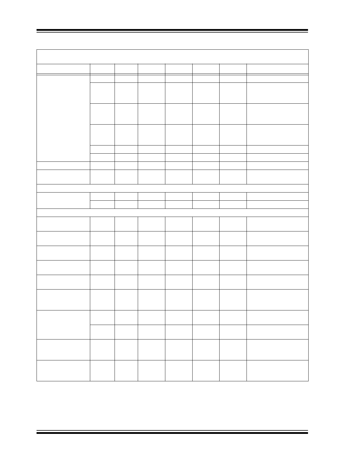
Push-to-Test (PTT)
Alarm Memory On
Time
T
HON4
13
9.8
10.4
11.0
ms
Alarm memory active,
PTT
PTT Alarm Memory
Horn Period
T
HPER4
13
235
250
265
ms
Alarm memory active,
PTT
Interconnect Signal Operation (IO)
IO Active Delay
T
IODLY1
12
—
0
—
s
From start of Local Alarm
to IO active
Remote Alarm Delay
with Temporal Horn
Pattern
T
IODLY2A
12
0.780
1.00
1.25
s
No Local Alarm,
from IO active to alarm
Remote Alarm Delay
with Continuous Horn
Pattern
T
IODLY2B
12
380
572
785
ms
No Local Alarm,
from IO active to alarm
IO Charge
Dump Duration
T
IODMP
12
1.23
1.31
1.39
s
At conclusion of Local
Alarm or test
IO Filter
T
IOFILT
12
—
—
313
ms
Standby, no alarm
Hush Timer Operation
Hush Timer Period
T
TPER
—
8.0
8.6
9.1
Min
No alarm
Low Battery
Hush Timer Period
T
TPERLB
—
7.73
8.22
8.71
Hours
No alarm
EOL
End-of-Life
Age Sample
T
EOL
—
314
334
354
Hours
EOL Enabled, Standby
Detection
IRED On Time
T
IRON
2
—
100
—
µs
Prog Bits 32,33 = 1,1
2
—
200
—
µs
Prog Bits 32,33 = 0,1
2
—
300
—
µs
Prog Bits 32,33 = 1,0
2
—
400
—
µs
Prog Bits 32,33 = 0,0
AC ELECTRICAL CHARACTERISTICS (CONTINUED)
AC Electrical Characteristics:
Unless otherwise indicated, all parameters apply at T
A
= -10° to +60°C, V
DD
= 3V,
V
BST
= 4.2V, Typical Application (unless otherwise noted) (
Note 1
to
Note 4
).
Parameter
Symbol Test Pin
Min.
Typ.
Max.
Units
Conditions
Note 1:
See timing diagram for Horn Pattern (
Figure 5-2
).
2:
T
PCLK
and T
IRON
are 100% production tested. All other AC parameters are verified by functional testing.
3:
Typical values are for design information only.
4:
Limits over the specified temperature range are not production tested and are based on characterization
data.
RE46C191
DS20005225E-page 10
2013-2017 Microchip Technology Inc.
TEMPERATURE SPECIFICATIONS
Electrical Specifications:
All limits specified for V
DD
= 3V, V
BST
= 4.2V, and V
SS
= 0V, except where noted in the
Electrical Characteristics.
Parameters
Sym.
Min.
Typ.
Max.
Units
Conditions
Temperature Ranges
Operating Temperature Range
T
A
-10
—
+60
°C
Storage Temperature Range
T
STG
-55
—
+125
°C
Thermal Package Resistances
Thermal Resistance, 16L-SOIC (150 mil.)
θ
JA
—
86.1
—
°C/W