
2011 Microchip Technology Inc.
DS22275A-page 1
RE46C180
Features
• 6 – 12V Operation
• Low Quiescent Current Consumption
• Programmable Standby Sensitivity
• Programmable HUSH Sensitivity
• Programmable Hysteresis
• Programmable Chamber Voltage for Push-to-Test
(PTT) and Chamber Test
• Programmable ±150 mV Low Battery Set Point
• Internal Ionization Chamber Test
• Internal Low Battery Test
• Internal Power-On Reset and Power-up Low
Battery Test
• Alarm Memory
• Auto Alarm Locate
• Horn Synchronization
• IO Filter and Charge Dump
• Smart Interconnect
• Interconnect up to 40 Detectors
• ±5% All Internal Oscillator
• 9 Minute or 80 Second Timer for Sensitivity
Control
• Temporal or Continuous Horn Pattern
• Guard Outputs for Ion Detector Input
• ±0.75 pA Detect Input Current
• 10-year End-of-Life Indication
Description
The RE46C180 is a next generation low power, CMOS
ionization-type, smoke detector IC. With minimal exter-
nal components, this circuit will provide all the required
features for an ionization-type smoke detector.
An on-chip oscillator strobes power to the smoke
detection circuitry for 5 ms every 10 seconds to keep
the standby current to a minimum.
A check for a Low Battery condition is performed every
80s and an ionization chamber test is performed once
every 320s when in Standby. The temporal horn pattern
complies with the National Fire Protection Association
NFPA 72
®
National Fire Alarm and Signaling Code
®
for
emergency evacuation signals.
An interconnect pin allows multiple detectors to be con-
nected, such that when one unit alarms, all units will
sound. A charge dump feature quickly discharges the
interconnect line when exiting a Local Alarm condition.
The interconnect input is also digitally filtered.
An internal 9 minute or 80s timer can be used for a
Reduced Sensitivity mode.
An alarm memory feature allows the user to determine
whether the unit has previously entered a Local Alarm
condition.
Utilizing low-power CMOS technology, the RE46C180
is designed for use in smoke detectors that comply with
the Standard for Single and Multiple Station Smoke
Alarms, UL217 and the Standard for Smoke Detectors
for Fire Alarm Systems, UL268.
Package Types
RE46C180
PDIP, SOIC
TEST
1
2
3
4
5
6
7
8
16
15
14
13
12
11
10
9
IO
GLED
CHAMBER
RLED
V
DD
TESTOUT
FEED
GUARD2
DETECT
GUARD1
T3
T2
HS
HB
V
SS
CMOS Programmable Ionization Smoke Detector ASIC with
Interconnect, Timer Mode and Alarm Memory
RE46C180
DS22275A-page 2
2011 Microchip Technology Inc.
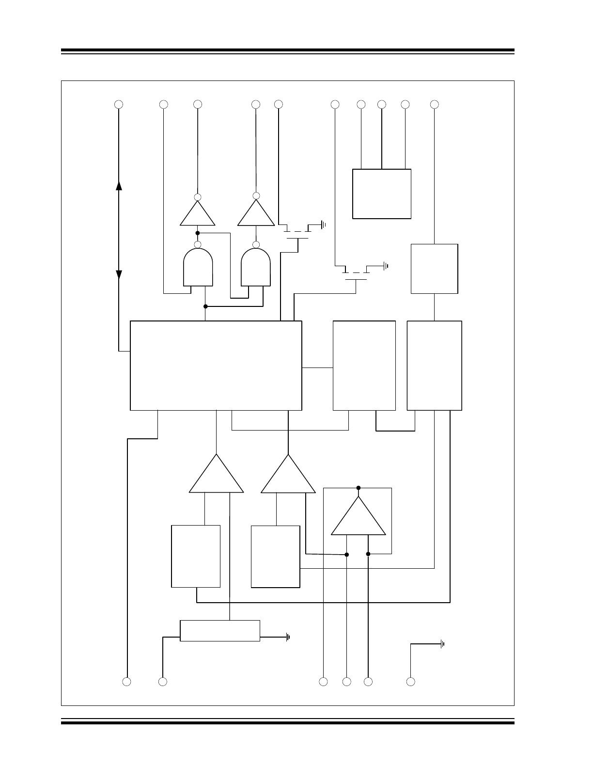
Functional Block Diagram
+
-
+
-
+
-
V
DD
(6)
TEST
(1)
GUARD1
(14)
DETECT
(15)
GUARD2
(16)
V
SS
(9)
IO
(2)
FEED
(8)
HS
(11)
RLED
(5)
HB
(10)
CHAMBER
(4)
T3
(13)
Logic
and
Timing
BIAS,
P
ower
Reset
and
Trimmable
Oscillator
Programmable
Trim
Trimmable
Low
B
att
Reference
Trimmable
Smoke
Reference
GLED
(3)
Chamber
Voltage
T2
(12)
TESTOUT
(7)
Test
and
Program
Mode
Sel
Low
B
att
Comp
Smoke
Comp
Guard
Amp
Trimmable
Low
B
att
Setting
2011 Microchip Technology Inc.
DS22275A-page 3
RE46C180
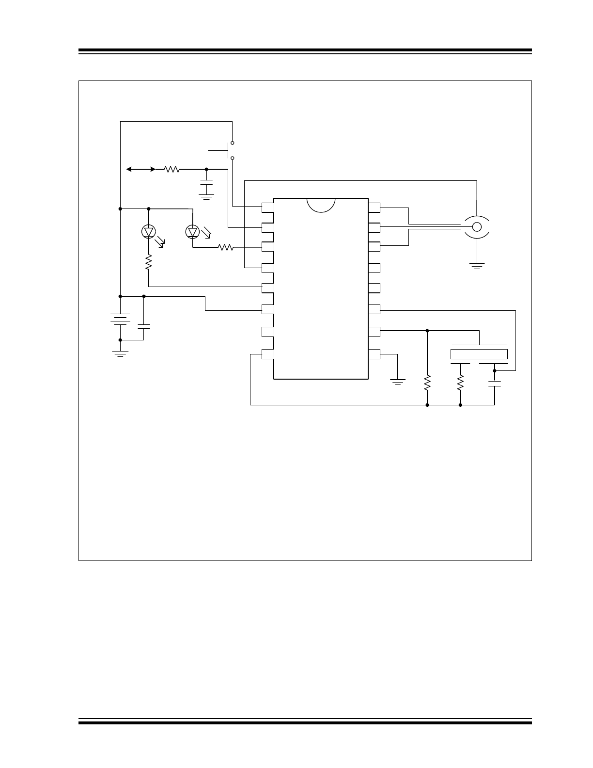
Typical Application
Note 1:
R3, R4 and C1 are typical values, and may be adjusted to maximize sound pressure.
2:
C2 should be located as close as possible to the device power pins.
3:
Route the pin 8 PC board trace away from pin 4 to avoid coupling.
4:
No internal reverse battery protection. External reverse battery protection circuitry required.
9V
Battery
+
-
1 µF
C2
R1
390
R5
100
To Other
Units
TEST and HUSH
R4
220K
R3
1.5M
C1
.001 µF
Rled
TEST
IO
GLED
CHAMBER
RLED
V
DD
TESTOUT
FEED
GUARD2
DETECT
GUARD1
T3
T2
HS
HB
V
SS
1
2
3
4
5
6
7
8
9
10
11
12
13
14
15
16
Gled
R2
390
RE46C180
C3
10 µF
RE46C180
DS22275A-page 4
2011 Microchip Technology Inc.
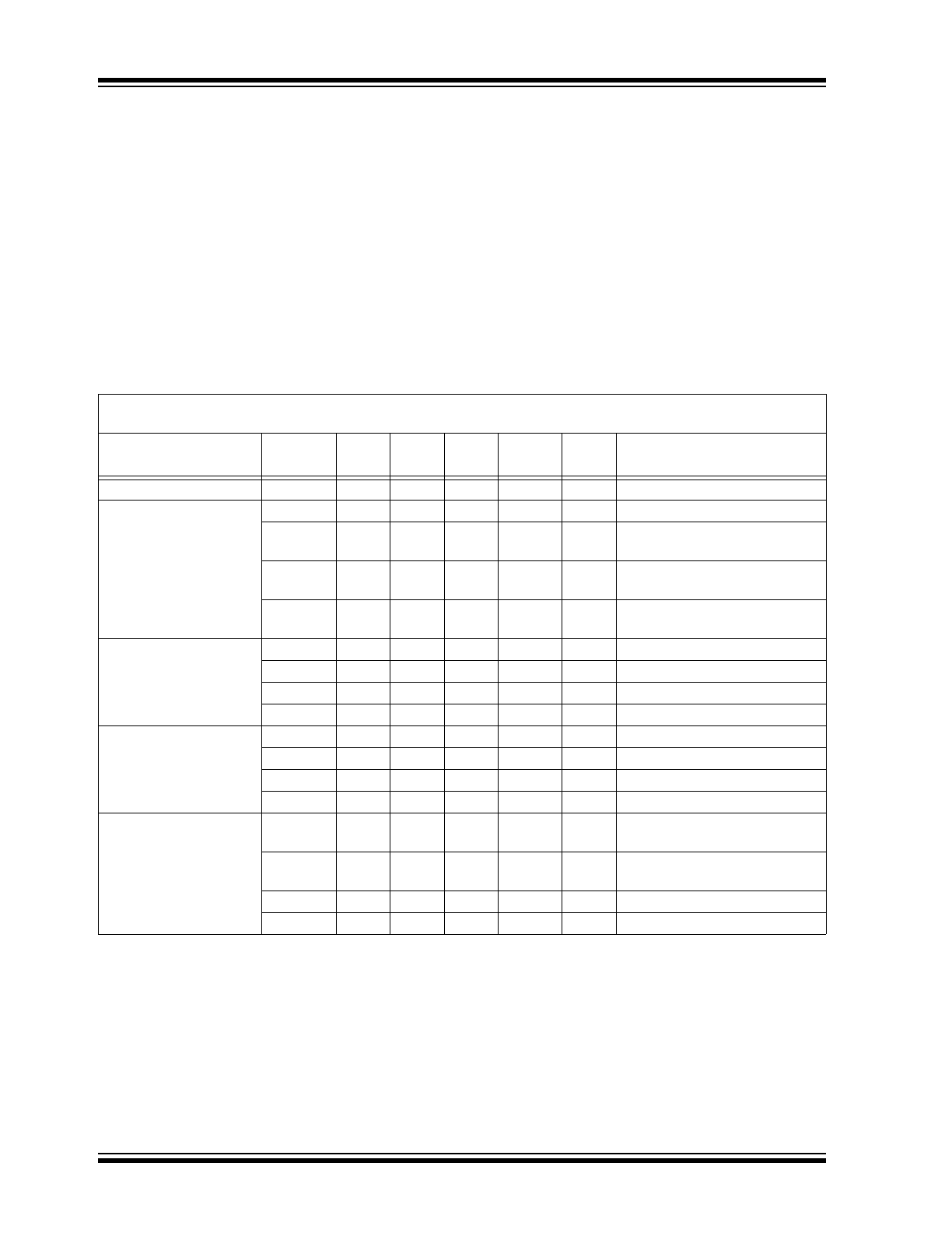
1.0
ELECTRICAL
CHARACTERISTICS
1.1
Absolute Maximum Ratings†
V
DD
.................................................................................12.5V
Input Voltage Range Except FEED, IO .......... V
IN
= -.3V to V
DD
+.3V
FEED Input Voltage Range ..................... V
INFD
=-10 to +22V
IO Input Voltage Range................................. V
IO1
= -.3 to 15V
Input Current except FEED ...................................I
IN
= 10 mA
Operating Temperature ................................T
A =
-10 to +60°C
Storage Temperature............................ T
STG
= -55 to +125°C
Maximum Junction Temperature ............................T
J
= +150°
† Notice:
Stresses above those listed under “Maximum
ratings” may cause permanent damage to the device.
This is a stress rating only and functional operation of
the device at these or any other conditions above those
indicated in the operation listings of this specification is
not implied. Exposure to maximum rating conditions for
extended periods may affect device reliability.
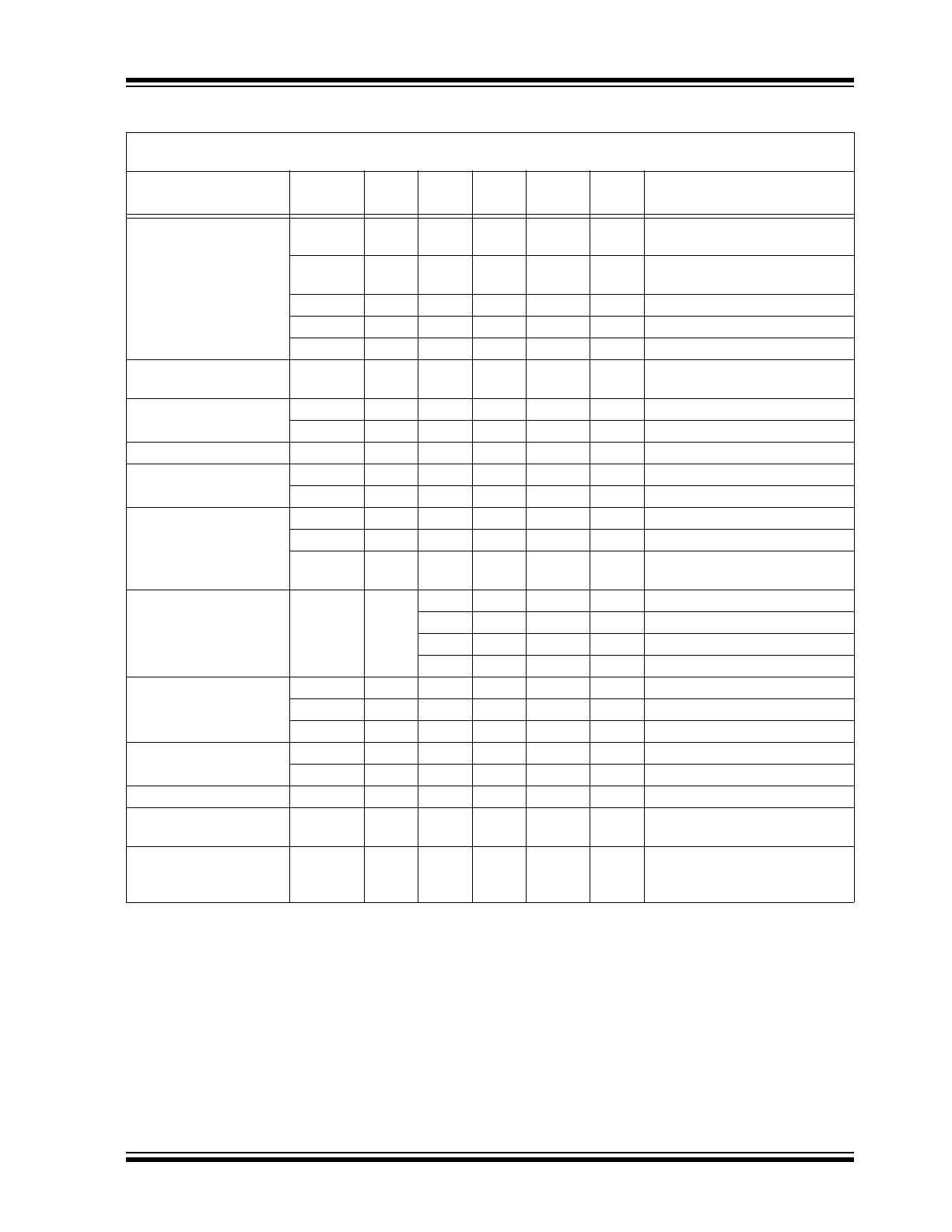
DC ELECTRICAL CHARACTERISTICS
DC Electrical Characteristics:
Unless otherwise indicated, all parameters apply at T
A
= -10°C to +60°C,
V
DD
= 9V, V
SS
= 0V (
Note 1
)
Parameter Symbol
Test
Pin
Min Typ Max Units
Conditions
Supply Voltage
V
DD
6
6
—
12
V
Operating
Supply Current
I
DD1
6
—
3.8
5.3
µA
Operating, RLED off, GLED off
I
DD2
6
—
—
6
µA
Operating, V
DD
= 12V,
RLED off, GLED off
I
DD3
6
—
9.6
13.9
µA
Operating, RLED off,
GLED off, Smoke check
I
DD4
6
—
21.4
30
µA
Operating, RLED off, GLED off,
Low Battery check
Input Voltage High
V
IH1
8
6
—
—
V
V
IH2
2
3
—
—
V
No Local Alarm, IO as an input
V
IH3
1
5.6
—
—
V
V
IH4
12
5.6
—
—
V
Input Voltage Low
V
IL1
8
—
—
2.8
V
V
IL2
2
—
—
1
V
No Local Alarm, IO as an input
V
IL3
1
—
—
3.4
V
V
IL4
12
—
—
3.4
Input Leakage Low
IL
DET1
15
—
—
-0.75
pA
V
DD
= 9V, DETECT = V
SS
,
0-40% RH, T
A
= +25°C
IL
DET2
15
—
—
-1.5
pA
V
DD
= 9V, DETECT = V
SS
,
85% RH, T
A
= +25°C (
Note 2
)
IL
FD1
8
—
—
-50
µA
FEED = -10V
IL
FD2
8
—
—
-100
nA
FEED = V
SS
Note 1:
Production tested at room temperature with temperature guard banded limits.
2:
Sample test only.
3:
Not 100% production tested.
4:
Same limit range at each programmable step, see
Table 4-1
.
2011 Microchip Technology Inc.
DS22275A-page 5
RE46C180
Input Leakage High
IH
DET1
15
—
—
0.75
pA
V
DD
= 9V, DETECT = V
DD
,
0–40% RH, T
A
= +25°C
IH
DET2
15
—
—
1.5
pA
V
DD
= 9V, DETECT = V
DD
,
85% RH, T
A
= +25°C (
Note 2
)
IH
FD1
8
—
—
50
µA
FEED = 22V
IH
FD2
8
—
—
100
nA
FEED = V
DD
I
IOL2
2
—
—
150
µA
No
Alarm,
V
IO
= 15V
Output Off Leakage High
I
IOHZ
3, 5
—
—
1
µA
Outputs Off,
V
RLED
= 9V, V
GLED
= 9V
Input Pull Down Current
I
PD1
1
20
50
80
µA
TEST = 9V
I
PD2
12
0.4
0.8
1.3
mA
T2 = 9V
Output High Voltage
V
OH1
10,11
6.3
—
—
V
I
OH
= -16 mA, V
DD
= 7.2V
Output Low Voltage
V
OL1
10,11
—
—
0.9
V
I
OL
= 16 mA, V
DD
= 7.2V
V
OL3
3, 5
—
—
1
V
I
OL
= 10 mA, V
DD
= 7.2V
Output Current
I
IOL1
2
25
—
60
µA
No
Alarm,
V
IO
= V
DD
-2V
I
IOH1
2
-4
—
-16
mA
Alarm,
V
IO
= 4V or V
IO
= 0V
I
IODMP
2
5
—
—
mA
At conclusion of Local Alarm
or PTT, V
IO
= 1V
Low Battery Voltage
V
LB
6
6.75
6.9
7.05
V
LBTR[2:1] = 1 0
7.05
7.2
7.35
V
LBTR[2:1] = 1 1
7.35
7.5
7.65
V
LBTR[2:1] = 0 0
7.65
7.8
7.95
V
LBTR[2:1] = 0 1
Offset Voltage
V
GOS1
14,15
-50
—
50
mV
Guard
amplifier
V
GOS2
15,16
-50
—
50
mV
Guard
amplifier
V
GOS3
15
-50
—
50
mV
Smoke
comparator
Common Mode Voltage
V
CM1
14,15
2
—
V
DD
–.5
V
Guard amplifier (
Note 3
)
V
CM2
15
0.5
—
V
DD
–2
V
Smoke comparator (
Note 3
)
Output Impedance
Z
OUT
14,16
—
10
—
k
Guard amplifier outputs (
Note 3
)
Chamber Voltage in
PTT/Chamber Test
V
CHAMBER
4
4.49
4.5
4.51
V
User programmable
(2.1V to 6.75V) (
Note 4
)
Hysteresis V
HYS
13
140
150
160
mV
No Alarm to Alarm condition,
user programmable
(50 to 225 mV) (
Note 4
)
DC ELECTRICAL CHARACTERISTICS (CONTINUED)
DC Electrical Characteristics:
Unless otherwise indicated, all parameters apply at T
A
= -10°C to +60°C,
V
DD
= 9V, V
SS
= 0V (
Note 1
)
Parameter Symbol
Test
Pin
Min Typ Max Units
Conditions
Note 1:
Production tested at room temperature with temperature guard banded limits.
2:
Sample test only.
3:
Not 100% production tested.
4:
Same limit range at each programmable step, see
Table 4-1
.
RE46C180
DS22275A-page 6
2011 Microchip Technology Inc.
AC ELECTRICAL CHARACTERISTICS
AC Electrical Characteristics:
Unless otherwise indicated, all parameters apply at T
A
= -10°C to +60°C,
V
DD
= 9V, V
SS
= 0V.
Parameter Symbol
Test
Pin
Min Typ Max
Units
Conditions
Time Base
Internal Oscillator Period
T
POSC
7
593
625
657
µs
Test mode (
Note 1
)
Internal Clock Period
T
PCLK
9.5
10
10.5
ms
Operating
RLED Indicator
On Time
T
ON1
5
9.5
10
10.5
ms
Operating
Period
T
PLED1
5
304
320
336
s
Standby
T
PLED2
5
0.95
1
1.05
s
Local alarm
T
PLED3
5
9.5
10
10.5
s
HUSH mode, No Local Alarm
GLED Indicator
Period
T
PLED4
3
38
40
42
s
Alarm Memory Indication
GLED period, No Alarm,
no PTT
T
PLED5
3
237
250
263
ms
Alarm Memory Indication
GLED period upon PTT,
AMLEDEn = 1
Off Time
T
OFLED1
3
0.95
1
1.05
s
Alarm Memory Indication
GLED off time between
pulses
T
OFLED2
3
36
38
40
s
Alarm Memory Indication
GLED off time between pulse
trains (3x)
Alarm Memory Indication
Timeout Period
T
AMTO
3
22.8
24
25.2
Hour
AMTO[2:1] = 0 0
45.6
48
50.4
Hour
AMTO[2:1] = 0 1
0
0
0
Hour
AMTO[2:1] = 1 0,
No Alarm Memory Indication
—
—
—
—
AMTO[2:1] = 1 1,
Alarm Memory Indication
never times out, as long as
Alarm Memory Latch is set
Smoke Check
Smoke Check Time
T
SCT
—
4.7
5
5.3
ms
Operating
Smoke Check Period
T
PER0
—
9.5
10
10.5
s
Standby, No Alarm
T
PER1
—
0.95
1
1.05
s
Standby, after one valid
smoke sample and before
entering Local Alarm, no PTT
T
PER2
—
237
250
263
ms
Standby, upon start of PTT
and before entering Local
Alarm
T
PER3
—
0.95
1
1.05
s
Local Alarm (after three con-
secutive valid smoke
samples) or Remote Alarm
Chamber Test Period
T
PCT1
—
304
320
336
s
Operating
Note 1:
T
POSC
is 100% production tested. All other timing is verified by functional testing.
2:
See timing diagram for CO alarm horn pattern.
3:
See timing diagram for smoke alarm temporal and non-temporal horn pattern.
4:
See timing diagram for horn synchronization and Auto Alarm Locate (AAL).
2011 Microchip Technology Inc.
DS22275A-page 7
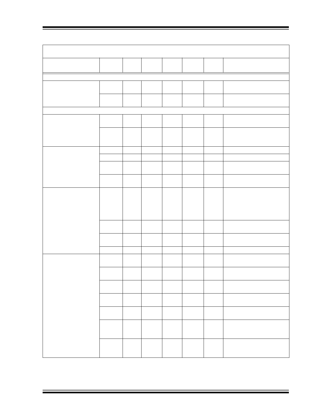
RE46C180
Low Battery
Low Battery Check
Period
T
PLB1
—
76
80
84
s
Standby, No Alarm,
No Low Battery
T
PLB2
—
304
320
336
s
Standby, No Alarm, Low
Battery
Horn Operation
Horn Delay
T
HDLY1
10, 11
475
500
525
ms
From Local Alarm to Horn
Active, temporal horn pattern
T
HDLY2
10, 11
380
400
420
ms
From Local Alarm to Horn
Active, continuous horn
pattern
Horn Period
T
HPER1
10, 11
38
40
42
s
Low Battery, No Alarm
T
HPER2
10, 11
38
40
42
s
Chamber Failure, No Alarm
T
HPER3
10, 11
237
250
263
ms
Alarm Memory Indication
upon PTT, AMHCEn=1
T
HPER4
10, 11
5.5
5.8
6.1
s
CO Alarm horn period
(
Note 2
)
Horn On Time
T
HON1
10, 11
9.5
10
10.5
ms
1.
Low Battery, No Alarm
2.
Chamber Failure
3.
Alarm Memory
Indication upon PTT,
AMHCEn = 1
T
HON2
10, 11
475
500
525
ms
Smoke Alarm, temporal horn
pattern (
Note 3
)
T
HON3
10, 11
332
350
368
ms
Smoke Alarm, continuous
horn pattern (
Note 3
)
T
HON4
10, 11
95
100
105
ms
CO Alarm, COEn = 1
Horn Off Time
T
HOF1
10, 11
475
500
525
ms
Smoke Alarm, temporal horn
pattern (
Note 3
)
T
HOF2
10, 11
1.43
1.5
1.58
s
Smoke Alarm, temporal horn
pattern (
Note 3
)
T
HOF3
10, 11
143
150
158
ms
Smoke Alarm, continuous
horn pattern (
Note 3
)
T
HOF4
10, 11
37
39
41
s
Chamber Fail horn off time
between pulse trains (3x)
T
HOF5
10, 11
465
490
515
ms
Chamber Fail horn off time
between pulses
T
HOF6
10, 11
95
100
105
ms
CO Alarm horn off time
between pulses,
COEn = 1 (
Note 2
)
T
HOF7
10, 11
4.8
5.1
5.4
s
CO alarm horn off time
between pulse trains,
COEn = 1 (
Note 2
)
AC ELECTRICAL CHARACTERISTICS
(CONTINUED)
AC Electrical Characteristics:
Unless otherwise indicated, all parameters apply at T
A
= -10°C to +60°C,
V
DD
= 9V, V
SS
= 0V.
Parameter Symbol
Test
Pin
Min Typ Max
Units
Conditions
Note 1:
T
POSC
is 100% production tested. All other timing is verified by functional testing.
2:
See timing diagram for CO alarm horn pattern.
3:
See timing diagram for smoke alarm temporal and non-temporal horn pattern.
4:
See timing diagram for horn synchronization and Auto Alarm Locate (AAL).

RE46C180
DS22275A-page 8
2011 Microchip Technology Inc.
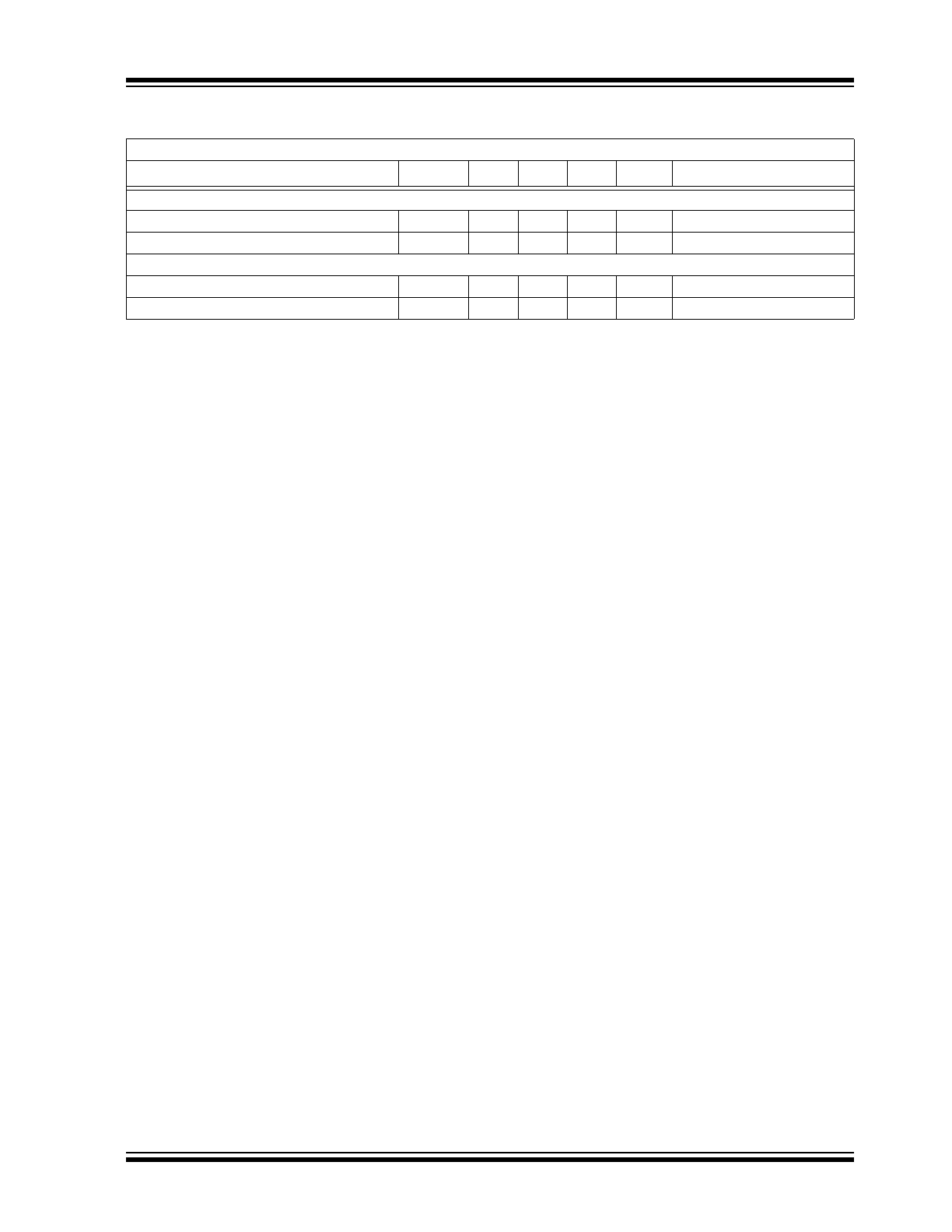
Interconnect
IO Active Delay
T
IODLY1
2
3.5
3.7
3.9
s
From start of Local Alarm
to IO Active. SyncEn = 1
2
3.1
3.3
3.5
s
From start of Local Alarm
to IO Active. SyncEn = 0
Remote Smoke Alarm
Delay
T
IODLY2
2
769
810
851
ms
No Local Alarm,
from IO Active to Alarm,
temporal horn pattern
T
IODLY3
2
299
315
331
ms
No Local Alarm,
from IO Active to alarm,
continuous horn pattern
IO Filter for Remote
Smoke Alarm
T
IOFILT
2
—
—
291
ms
IO pulse-width to be filtered
IO as input, no Local Alarm
IO Pulse On Time
for CO Alarm
T
IOPW1
2
37
—
290
ms
No Local Alarm, 2 valid
pulses required for CO
IO Pulse Off Time
for CO Alarm
T
IOTO1
2
—
—
5.4
s
IO = Low
IO Dump
T
IODMP1
2
475
500
525
ms
At conclusion of Local Alarm
or PTT
Horn Synchronization
IO Pulse Period
T
PIO1
2
3.8
4
4.2
s
Local Alarm, temporal horn
pattern, SyncEn =1 (
Note 4
)
IO Pulse On Time
T
ONIO
2
3.41
3.59
3.77
s
Local Alarm, temporal horn
pattern, SyncEn =1 (
Note 4
)
Horn Sync IO Dump
T
IODMP2
2
95
100
105
ms
Local Alarm,
SyncEn =1 (
Note 4
)
Horn Sync IO Dump
Delay
T
IODLY4
2
285
300
315
ms
Local Alarm,
SyncEn =1 (
Note 4
)
Auto Alarm Locate (AAL)
IO Cycle Period
T
PIO2
2
15.2
16
16.8
s
Local Alarm, temporal horn
pattern, SyncEn =1,
NoAAL = 0 (
Note 4
)
IO Cycle Off Time
T
OFIO
2
4.19
4.41
4.63
s
Local Alarm, temporal horn
pattern, SyncEn = 1,
No AAL = 0, IO off time
between IO pulse trains (3x)
(
Note 4
)
HUSH Timer Operation
HUSH Timer Period
T
TPER
—
8.5
9
9.5
min
No Alarm, ShrtTO = 0
—
76
80
84
s
No Alarm, ShrtTO = 1
EOL
End-of-Life Age Sample
T
EOL
—
346
364
382
Hours Standby, EOLEn = 1
AC ELECTRICAL CHARACTERISTICS
(CONTINUED)
AC Electrical Characteristics:
Unless otherwise indicated, all parameters apply at T
A
= -10°C to +60°C,
V
DD
= 9V, V
SS
= 0V.
Parameter Symbol
Test
Pin
Min Typ Max
Units
Conditions
Note 1:
T
POSC
is 100% production tested. All other timing is verified by functional testing.
2:
See timing diagram for CO alarm horn pattern.
3:
See timing diagram for smoke alarm temporal and non-temporal horn pattern.
4:
See timing diagram for horn synchronization and Auto Alarm Locate (AAL).
2011 Microchip Technology Inc.
DS22275A-page 9
RE46C180
TEMPERATURE CHARACTERISTICS
Electrical Specifications:
Unless otherwise indicated, V
DD
= 9V, V
SS
= 0V
Parameters
Sym
Min
Typ
Max
Units
Conditions
Temperature Ranges
Operating Temperature Range
T
A
-10
—
+60
°C
Storage Temperature Range
T
STG
-55
—
+125
°C
Thermal Package Resistances
Thermal Resistance, 16L-PDIP
θJ
A
—
70
—
°C/W
Thermal Resistance, 16L-SOIC (150 mil.)
θJ
A
—
86.1
—
°C/W

RE46C180
DS22275A-page 10
2011 Microchip Technology Inc.
2.0
PIN DESCRIPTIONS
The descriptions of the pins are listed in
Table 2-1
.
TABLE 2-1:
PIN FUNCTION TABLE
RE46C180
PDIP, SOIC
Symbol
Function
1
TEST
This input is used to invoke Push-to-Test, Timer mode and Alarm Memory
Indication. This input has an internal pull-down.
2
IO
This bidirectional pin provides the capability to interconnect many detectors
in a single system. This pin has an internal pull-down device and a charge
dump device.
3
GLED
Open drain NMOS output, used to drive a visible LED to provide visual
indication of an Alarm Memory condition.
4
CHAMBER
Connect to the ionization smoke chamber. This pin provides power to the
chamber
5
RLED
Open drain NMOS output, used to drive a visible LED. This pin provides the
load current for the Low Battery test, and is a visual indicator for alarm and
HUSH mode.
6
V
DD
Connect to the positive supply voltage
7
TESTOUT
This output is an indicator of the internal IO dump signal. This pin is also
used for Test modes.
8
FEED
Usually connected to the feedback electrode through a current limiting
resistor. If not used, this pin must be connected to V
DD
or V
SS
.
9
V
SS
Connect to the negative supply voltage.
10
HB
This pin is connected to the metal electrode of a piezoelectric transducer.
11
HS
This pin is a complementary output to HB, connected to the ceramic
electrode of the piezoelectric transducer.
12
T2
Test input to invoke Test modes. This pin has an internal pull-down.
13
T3
Test output for Test modes.
14
GUARD1
Output of the guard amplifier. This allows for measurement of the DETECT
input without loading the ionization chamber.
15
DETECT
Connect to the CEV of the ionization smoke chamber.
16
GUARD2
Output of the guard amplifier. This allows for measurement of the DETECT
input without loading the ionization chamber.