

2010-2016 Microchip Technology Inc.
DS20002251B-page 1
RE46C165/6/7/8
Features
• Temporal Horn Pattern or Continuous Tone
• Alarm Memory
• Sensitivity Control Times:
- 9 minutes (RE46C165/6)
- 1.2 minutes (RE46C167/8)
• I/O Filter and Charge Dump
• Interconnect up to 40 Detectors
• Internal Power-on Reset (POR)
• >2000V ESD Protection (HBM) on All Pins
• Low Quiescent Current Consumption (<8 µA)
• Internal Low Battery Detection and Chamber Test
• RoHS Compliant Lead-Free Packaging
Description
The RE46C165/6/7/8 devices are low-power, CMOS
photoelectric type, smoke detector ICs. With minimal
external components, these circuits will provide all the
required features for a photoelectric type smoke
detector.
Each design incorporates a gain-selectable photo
amplifier for use with an infrared emitter/detector pair.
An internal oscillator strobes power to the smoke
detection circuitry for 100 µs, every 10 seconds, to
keep standby current to a minimum. If smoke is
sensed, the detection rate is increased to verify an
alarm condition. A High-Gain mode is available for
push button chamber testing.
A check for a low battery condition and chamber
integrity is performed every 43 seconds when in
standby. The temporal horn pattern supports the
NFPA 72 emergency evacuation signal.
An interconnect pin allows multiple detectors to be
connected so when one unit alarms, all units will sound.
A charge dump feature will quickly discharge the
interconnect line when exiting a local alarm. The
interconnect input is also digitally filtered.
An internal timer allows for single button, push-to-test
to be used for a Reduced Sensitivity mode.
An alarm memory feature allows the user to determine
if the unit has previously entered a local alarm
condition.
Utilizing low-power CMOS technology, the
RE46C165/6/7/8 was designed for use in smoke
detectors that comply with Underwriters Laboratory
Specification UL217 and UL268.
CMOS Photoelectric Smoke Detector ASIC
with Interconnect, Timer Mode and Alarm Memory
RE46C165/6/7/8
DS20002251B-page 2
2010-2016 Microchip Technology Inc.
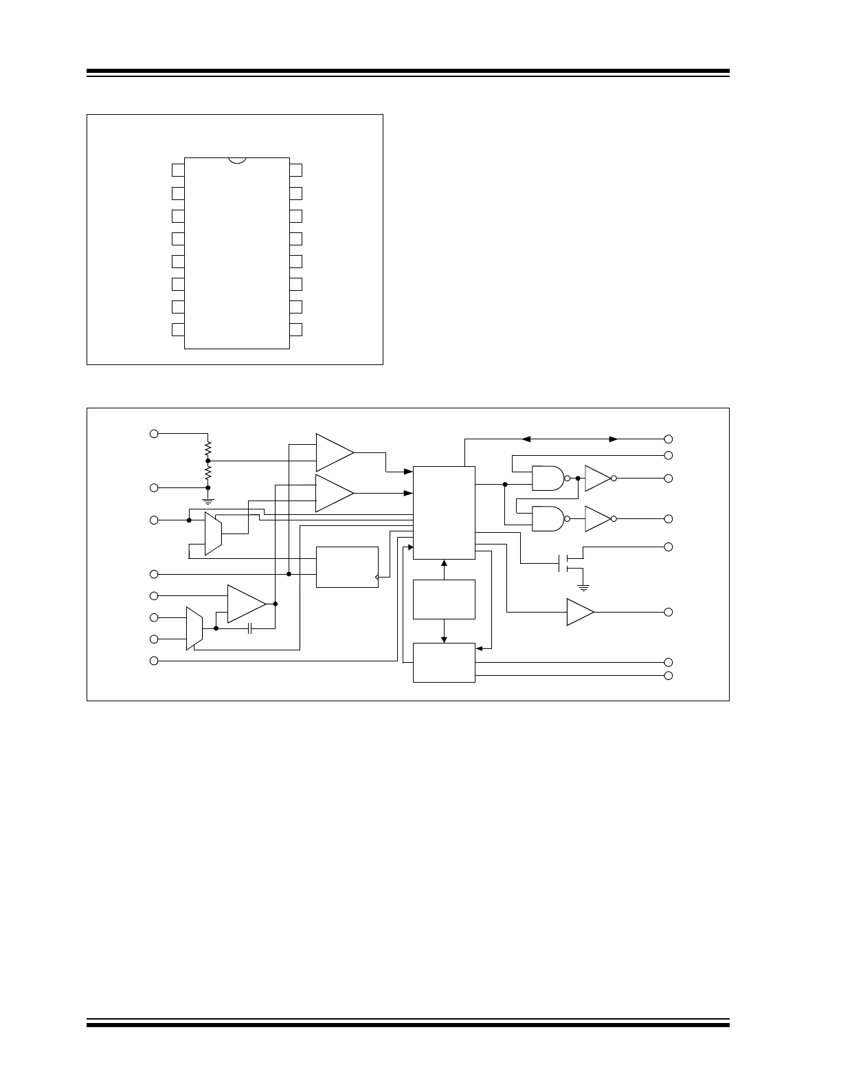
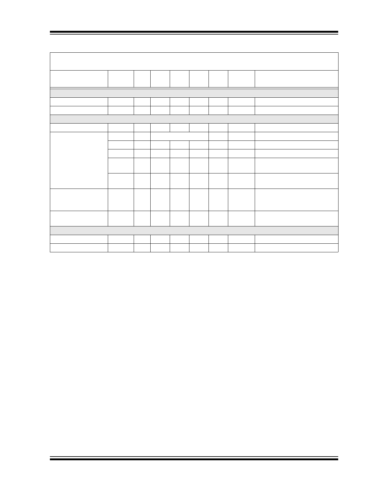
Package Types
Functional Block Diagram
RE46C165/6/7/8
PDIP, SOIC
C1
1
2
3
4
5
6
7
8
16
15
14
13
12
11
10
9
C2
DETECT
STROBE
V
DD
IRED
IO
HORNB
TEST
VSEN
V
SS
ROSC
COSC
LED
FEED
HORNS
Logic
and
Timing
Bias and
Power
Reset
+
–
+
–
V
DD
(5)
VSEN (15)
C1 (1)
DETECT (3)
C2 (2)
TEST (16)
R2
124K
R1
276K
IO (7)
FEED (10)
HS (9)
LED (11)
IRED (6)
ROSC (13)
COSC (12)
HB (8)
+
–
STROBE (4)
V
DD
– 5V
V
DD
– 3.5V
Photoamp
V
SS
(14)
Reference
Oscillator
2010-2016 Microchip Technology Inc.
DS20002251B-page 3
RE46C165/6/7/8
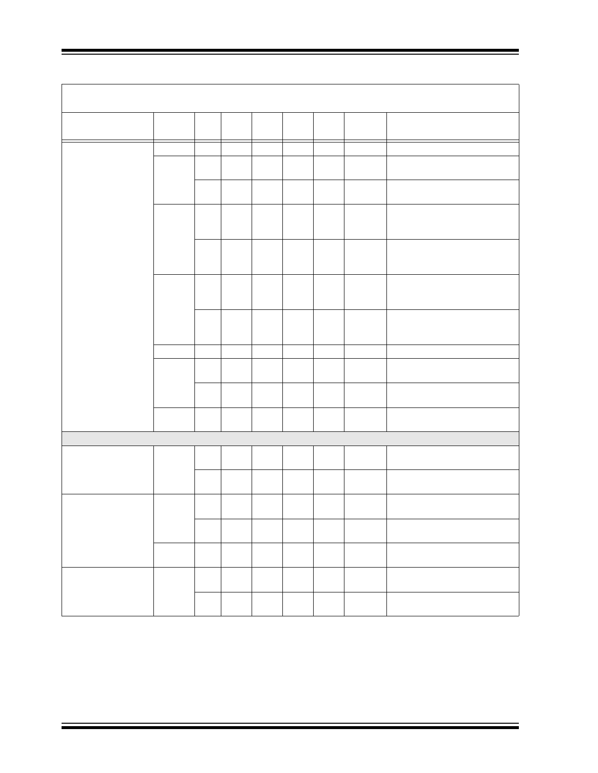
Typical Application
Push-to-Test
9V
Battery
C3
(1,2)
1 µF
C5
1.5 nF
R12
10M
R9
100k
R13
330
D3
C6
(3)
1.0 nF
R10
(3)
1.5M
R11
(3)
220k
R8
330
C7
10 µF
R7
22
C4
100 µF
D5
D6
R4
560
C2 4.7 nF
C1 47 nF
R1
4.7k
R2
5k
R3
8.2k
R
ADJ2
120k
R
ADJ1
1.0M
R6 1k
C1
C2
DETECT
STROBE
V
DD
V
SS
IRED
IO
HORNB
HORNS
FEED
LED
COSC
ROSC
VSEN
TEST
R5
249k
To Other Units
1
2
3
4
5
6
7
8
16
15
14
13
12
11
10
9
Note 1:
C3 should be located as close as possible to the device power pins.
2:
C3 is typical for an alkaline battery. This capacitance should be increased to 4.7 µF or greater for a carbon battery.
3:
R10, R11 and C6 are typical values and may be adjusted to maximize sound pressure.
Q3
Photo
Chamber

RE46C165/6/7/8
DS20002251B-page 4
2010-2016 Microchip Technology Inc.
NOTES:
2010-2016 Microchip Technology Inc.
DS20002251B-page 5
RE46C165/6/7/8
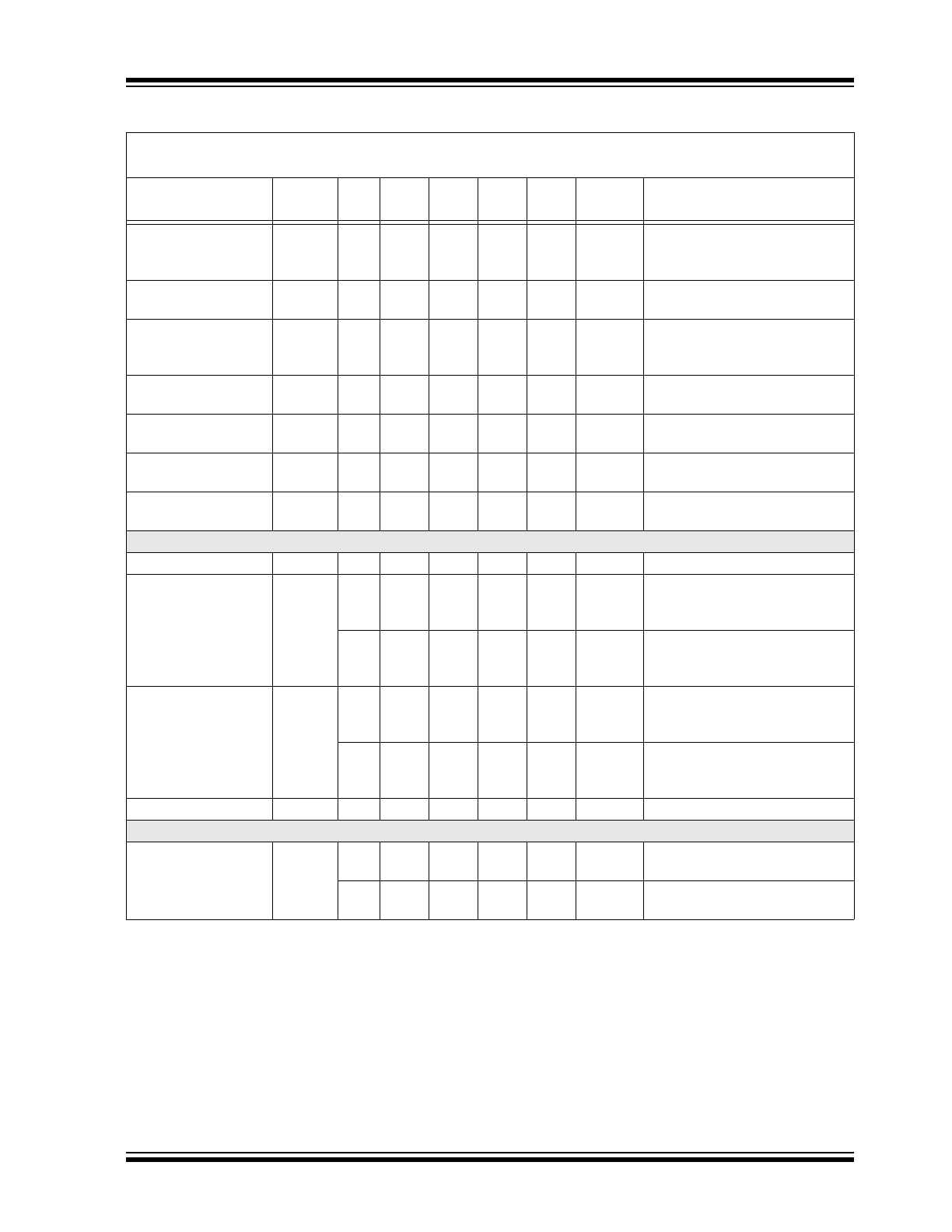
1.0
ELECTRICAL
CHARACTERISTICS
Absolute Maximum Ratings
†
V
DD
................................................................................... 12.5V
Input Voltage Range except FEED, I/O......V
IN
= -0.3V to V
DD
+ 0.3V
FEED Input Voltage Range....................... V
INFD
= -10 to +22V
I/O Input Voltage Range..................................V
IO1
= -0.3 to 15V
Input Current except FEED, TEST, VSEN ............... I
IN
= 10 mA
Input Current for FEED, VSEN ............................... I
IN
= 500 µA
Operating Temperature ...................................T
A =
-25 to +75°C
Storage Temperature ...............................T
STG
= -55 to +125°C
Maximum Junction Temperature............................ T
J
= +150°C
† Notice:
Stresses above those listed under “Maximum
Ratings” may cause permanent damage to the device.
This is a stress rating only and functional operation of
the device at these, or any other conditions above those
indicated in the operation listings of this specification, is
not implied. Exposure to maximum rating conditions for
extended periods may affect device reliability.
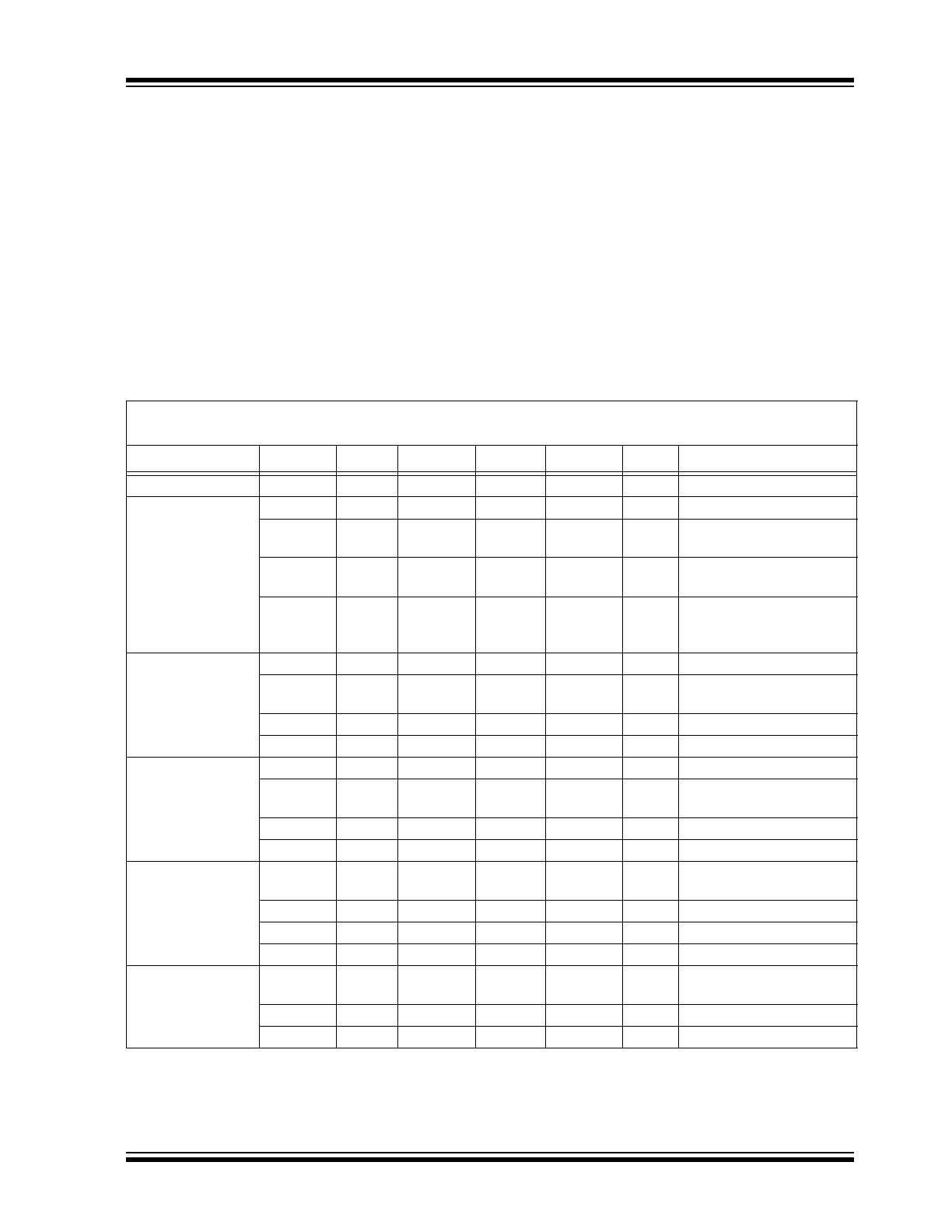
DC ELECTRICAL CHARACTERISTICS
(
3
)
DC Electrical Characteristics:
Unless otherwise indicated, all parameters apply at T
A
= -25° to +75°, V
DD
= 9V,
Typical Application (unless otherwise noted), V
SS
= 0V
Parameter
Symbol
Test Pin
Min.
Typ.
Max.
Units
Conditions
Supply Voltage
V
DD
5
6
—
12
V
Operating
Supply Current
I
DD1
5
—
4
6
µA
COSC = V
SS
, LED off
I
DD2
5
—
5.5
8
µA
COSC = V
SS
, LED off,
V
DD
= 12V
I
DD3
5
—
—
2
mA
COSC = V
SS
,
STROBE on IRED off
I
DD4
5
—
—
3
mA
COSC = V
SS
,
STROBE on, IRED on
(
Note 1
)
Input Voltage High
V
IH1
10
6.2
4.5
—
V
FEED
V
IH2
7
3.2
—
—
V
No local alarm,
I/O as an input
V
IH3
15
1.6
—
—
V
VSEN
V
IH4
16
8.5
—
—
V
TEST
Input Voltage Low
V
IL1
10
—
4.5
2.7
V
FEED
V
IL2
7
—
—
1.5
V
No local alarm,
I/O as an input
V
IL3
15
—
— 0.5
V
VSEN
V
IL4
16
—
— 7
V
TEST
Input Leakage Low
I
IL1
1, 2, 3
—
—
-100
nA
V
DD
= 12V, COSC = 12V,
STROBE active
I
IL2
12, 10
—
—
-100
nA
V
DD
= 12V, V
IN
= V
SS
I
IL3
15, 16
—
—
-1
µA
V
DD
= 12V, V
IN
= V
SS
I
LFD
10
—
—
-50
µA
FEED = -10V
Input Leakage High
I
IH1
1, 2
—
—
100
nA
V
DD
= 12V, V
IN
= V
DD
,
STROBE active
I
IH2
3, 10, 12
—
—
100
nA
V
DD
= 12V, V
IN
= V
DD
I
HFD
10
—
—
50
µA
FEED = 22V
Note 1:
Does not include Q3 emitter current.
2:
Not production tested.
3:
Production tested at room temperature with guardbanded limits.
RE46C165/6/7/8
DS20002251B-page 6
2010-2016 Microchip Technology Inc.
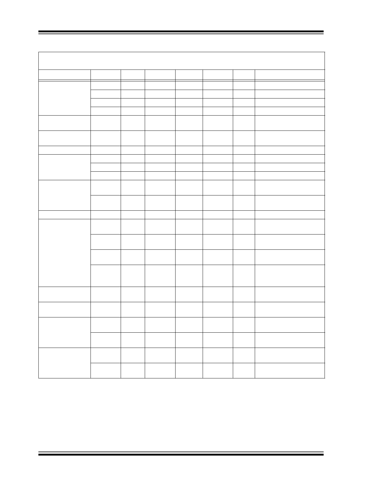
Input Pull-Down
Current
I
PD1
16
0.25
—
10
µA
V
IN
= V
DD
I
PD2
15
0.1
0.25
0.5
µA
V
IN
= V
DD
I
PDIO1
7
20
—
80
µA
V
IN
= V
DD
I
PDIO2
7
—
—
140
µA
V
IN
= 15V, V
DD
= 12V
Output Off Leakage
Low
I
OZL1
11, 13
—
—
-1
µA
Outputs off, Output = V
SS
Output Off Leakage
High
I
OZH1
11, 13
—
—
1
µA
Outputs off, Output = V
DD
Output High Voltage
V
OH1
8, 9
5.5
—
—
V
I
OH
= -16 mA, V
DD
= 6.5V
Output Low Voltage
V
OL1
8, 9
—
—
1
V
I
OL
= 16 mA, V
DD
= 6.5V
V
OL2
13
—
0.5
—
V
I
OL
= 5 mA, V
DD
= 6.5V
V
OL3
11
—
—
0.6
V
I
OL
= 10 mA, V
DD
= 6.5V
Output Current
I
IOH1
7
-4
—
-16
mA
Alarm, V
IO
= V
DD
– 2V
or V
IO
= 0V
I
IODMP
7
5
—
—
mA
At conclusion of local alarm
or test, V
IO
= 1V
Low Battery Voltage
V
LB
5
6.9
7.2
7.5
V
Output Voltage
V
STOF
4
V
DD
– 0.1
—
—
V
STROBE off, V
DD
= 12V,
I
OUT
= -1 µA
V
STON
4
V
DD
– 5.25 V
DD
– 5 V
DD
– 4.75
V
STROBE on, V
DD
= 9V,
I
OUT
= 100 µA to 500 µA
V
IREDOF
6
—
—
0.1
V
IRED off, V
DD
= 12V,
I
OUT
= 1 µA
V
IREDON
6
2.85
3.1
3.35
V
IRED on, V
DD
= 9V,
I
OUT
= 0 to -6 mA,
T
A
= +25°C
Common-Mode
Voltage
V
CM1
1, 2, 3
0.5
—
V
DD
– 2
V
Local smoke, push-to-test
or chamber test (
Note 2
)
Smoke Comparator
Reference
V
REF
—
V
DD
– 3.7 V
DD
– 3.5 V
DD
– 3.3
V
Internal reference (
Note 2
)
Temperature
Coefficient
TC
ST
4
—
0.01
—
%/°C STROBE output voltage,
V
DD
= 6V to 12V
TC
IRED
6
—
0.3
—
%/°C IRED output voltage,
V
DD
= 6V to 12V
Line Regulation
V
STON
4, 5
—
-50
—
dB
STROBE output (vs. V
DD
),
V
DD
= 6V to 12V
V
IREDON
6, 5
—
-30
—
dB
IRED output voltage,
V
DD
= 6V to 12V
DC ELECTRICAL CHARACTERISTICS
(
3
)
(CONTINUED)
DC Electrical Characteristics:
Unless otherwise indicated, all parameters apply at T
A
= -25° to +75°, V
DD
= 9V,
Typical Application (unless otherwise noted), V
SS
= 0V
Parameter
Symbol
Test Pin
Min.
Typ.
Max.
Units
Conditions
Note 1:
Does not include Q3 emitter current.
2:
Not production tested.
3:
Production tested at room temperature with guardbanded limits.
2010-2016 Microchip Technology Inc.
DS20002251B-page 7
RE46C165/6/7/8
AC ELECTRICAL CHARACTERISTICS
AC Electrical Characteristics:
Unless otherwise indicated, all parameters apply at T
A
= -25° to +75°, V
DD
= 9V,
Typical Application (unless otherwise noted), V
SS
= 0V.
Parameter
Symbol
Test
Pin
Min.
Typ.
Max.
Units
Clocks
Conditions
Oscillator Time Base (COSC, ROSC)
Oscillator Period
T
POSC
9
9.38
10.42 11.46
ms
1
Operating (
Note 1
)
Oscillator Tolerance
T
TOLOSC
9
-10
0
10
%
1
Operating
LED Indication (LED)
LED On Time
T
ON1
11
9.4
10.4
11.5
ms
1
Operating
LED Period
T
PLED0
11
LED IS NOT ON
s
—
Remote alarm only
T
PLED1
11
38
43
47
s
4096
Standby, no alarm
T
PLED2
11
450
500
550
ms
48
Local alarm condition
T
PLED3
11
9.6
10.7
11.7
s
1024
Timer mode, no local alarm
(
Note 4
)
T
PLED4
11
225
250
275
ms
24
Timer mode, no local alarm
(
Note 4
)
Alarm Memory LED
Pulse Train (3x)
Off Time
T
OFLED
11
1.2
1.3
1.5
s
127
Alarm memory set,
LED enabled
Alarm Memory LED
Timer Period
T
LALED
11
21.5
23.9
26.3
Hours 8257536 Alarm memory set
Detection (STROBE, IRED)
STROBE On Time
T
STON
4
9.4
10.4
11.5
ms
1
Smoke test, chamber test
IRED On Time
T
IRON
6
94
104
114
µs
0.01
Operating/DIAG (
Note 1
)
Note 1:
T
POSC
and T
IRON
are 100% production tested. All other timing is verified by functional testing.
2:
See the timing diagram for Horn Temporal Pattern in
Figure 3-2
.
3:
See the timing diagram for Horn Continuous Pattern in
Figure 3-3
.
4:
During Timer mode, the LED period is 10.5 seconds. The LED period will return to 43 seconds at the
conclusion of the Timer mode.
RE46C165/6/7/8
DS20002251B-page 8
2010-2016 Microchip Technology Inc.
Smoke Test Period
(IRED and STROBE)
T
PER0
4, 6
9.6
10.7
11.7
s
1024
Standby, no alarm
T
PER1
4, 6
1.8
2.0
2.2
s
192
RE46C165/7 only
Standby, 1 valid smoke sample
4, 6
2.4
2.7
2.9
s
256
RE46C166/8 only
Standby, 1 valid smoke sample
T
PER2
4, 6
0.9
1.0
1.1
s
96
RE46C165/7 only
Standby, after 2 consecutive
valid smoke samples
4, 6
1.2
1.3
1.5
s
128
RE46C166/8 only
Standby, after 2 consecutive
valid smoke samples
T
PER3
4, 6
0.9
1.0
1.1
s
96
RE46C165/7 only
Local alarm (3 consecutive valid
smoke samples)
4, 6
1.2
1.3
1.5
s
128
RE46C166/8 only
Local alarm (3 consecutive valid
smoke samples)
T
PER4
4, 6
300
333
367
ms
32
Push button test
T
PER5
4, 6
7.2
8.0
8.8
s
768
RE46C165/7 only
In remote alarm
4, 6
9.6
10.7
11.7
s
1024
RE46C166/8 only
In remote alarm
T
PER6
4, 6
38
43
47
s
4096
Chamber test or low battery test,
no alarm
Horn Operation (HORNB, HORNS, FEED)
Alarm On Time
T
HON1
8, 9
450
500
550
ms
48
RE46C165/7 only
Local or remote alarm (
Note 2
)
8, 9
225
250
275
ms
24
RE46C166/8 only
Local or remote alarm (
Note 3
)
Alarm Off Time
T
HOF1
8, 9
450
500
550
ms
48
RE46C165/7 only
Local or remote alarm (
Note 2
)
8, 9
75
83
92
ms
8
RE46C166/8 only
Local or remote alarm (
Note 3
)
T
HOF2
8, 9
1.35
1.50
1.65
s
144
RE46C165/7 only
Local or remote alarm (
Note 2
)
Alarm Period
T
HPER1
8, 9
3.60
4.00
4.40
s
384
RE46C165/7 only
Local or remote alarm (
Note 2
)
8, 9
0.30
0.33
0.37
s
32
RE46C166/8 only
Local or remote alarm (
Note 3
)
AC ELECTRICAL CHARACTERISTICS (CONTINUED)
AC Electrical Characteristics:
Unless otherwise indicated, all parameters apply at T
A
= -25° to +75°, V
DD
= 9V,
Typical Application (unless otherwise noted), V
SS
= 0V.
Parameter
Symbol
Test
Pin
Min.
Typ.
Max.
Units
Clocks
Conditions
Note 1:
T
POSC
and T
IRON
are 100% production tested. All other timing is verified by functional testing.
2:
See the timing diagram for Horn Temporal Pattern in
Figure 3-2
.
3:
See the timing diagram for Horn Continuous Pattern in
Figure 3-3
.
4:
During Timer mode, the LED period is 10.5 seconds. The LED period will return to 43 seconds at the
conclusion of the Timer mode.
2010-2016 Microchip Technology Inc.
DS20002251B-page 9
RE46C165/6/7/8
Low Battery
or Chamber Fail
Horn On Time
T
HON2
8, 9
9.4
10.4
11.5
ms
1
Low battery or fail chamber test,
no alarm
Low Battery
Horn Off Time
T
HOF3
8, 9
38
43
47
s
4095
Low battery, no alarm
Low Battery
or Chamber Fail
Period
T
HPER2
8, 9
38
43
47
s
4096
Low battery, no alarm
Chamber Fail
Horn Off Time
T
HOF4
8, 9
291
323
355
ms
31
Failed chamber, no alarm
Chamber Fail
Pause Off Time
T
HOF5
8, 9
38
42
46
s
4031
Failed chamber, no alarm
Push-to-Test Alarm
Memory Off Time
T
HOF6
8, 9
216
240
264
ms
23
Alarm memory active,
push-to-test
Push-to-Test Alarm
Memory Period
T
HPER3
8, 9
225
250
275
ms
24
Alarm memory active,
push-to-test
Interconnect Signal Operation (I/O)
I/O Active Delay
T
IODLY1
7
0.0
0.0
0.0
s
0
Local alarm start to I/O active
Remote Alarm Delay
T
IODLY2
7
0.74
0.99
1.27
s
95
RE46C165/7 only
No local alarm,
I/O active to alarm
7
0.37
0.57
0.81
s
55
RE46C166/8 only
No local alarm,
I/O active to alarm
I/O Charge
Dump Duration
T
IODMP
7
0.89
0.99
1.09
s
95
RE46C165/7 only
At conclusion of local alarm
or test
7
1.19
1.32
1.46
s
127
RE46C166/8 only
At conclusion of local alarm
or test
I/O Filter
T
IOFILT
7
—
—
0.30
s
32
Maximum I/O pulse width filtered
Hush Timer Operation
Hush Timer Period
T
TPER
—
8.1
9.0
9.9
Min
51712
RE46C165/6 only
No alarm condition
—
1.1
1.2
1.4
Min
7232
RE46C167/8 only
No alarm condition
AC ELECTRICAL CHARACTERISTICS (CONTINUED)
AC Electrical Characteristics:
Unless otherwise indicated, all parameters apply at T
A
= -25° to +75°, V
DD
= 9V,
Typical Application (unless otherwise noted), V
SS
= 0V.
Parameter
Symbol
Test
Pin
Min.
Typ.
Max.
Units
Clocks
Conditions
Note 1:
T
POSC
and T
IRON
are 100% production tested. All other timing is verified by functional testing.
2:
See the timing diagram for Horn Temporal Pattern in
Figure 3-2
.
3:
See the timing diagram for Horn Continuous Pattern in
Figure 3-3
.
4:
During Timer mode, the LED period is 10.5 seconds. The LED period will return to 43 seconds at the
conclusion of the Timer mode.
RE46C165/6/7/8
DS20002251B-page 10
2010-2016 Microchip Technology Inc.
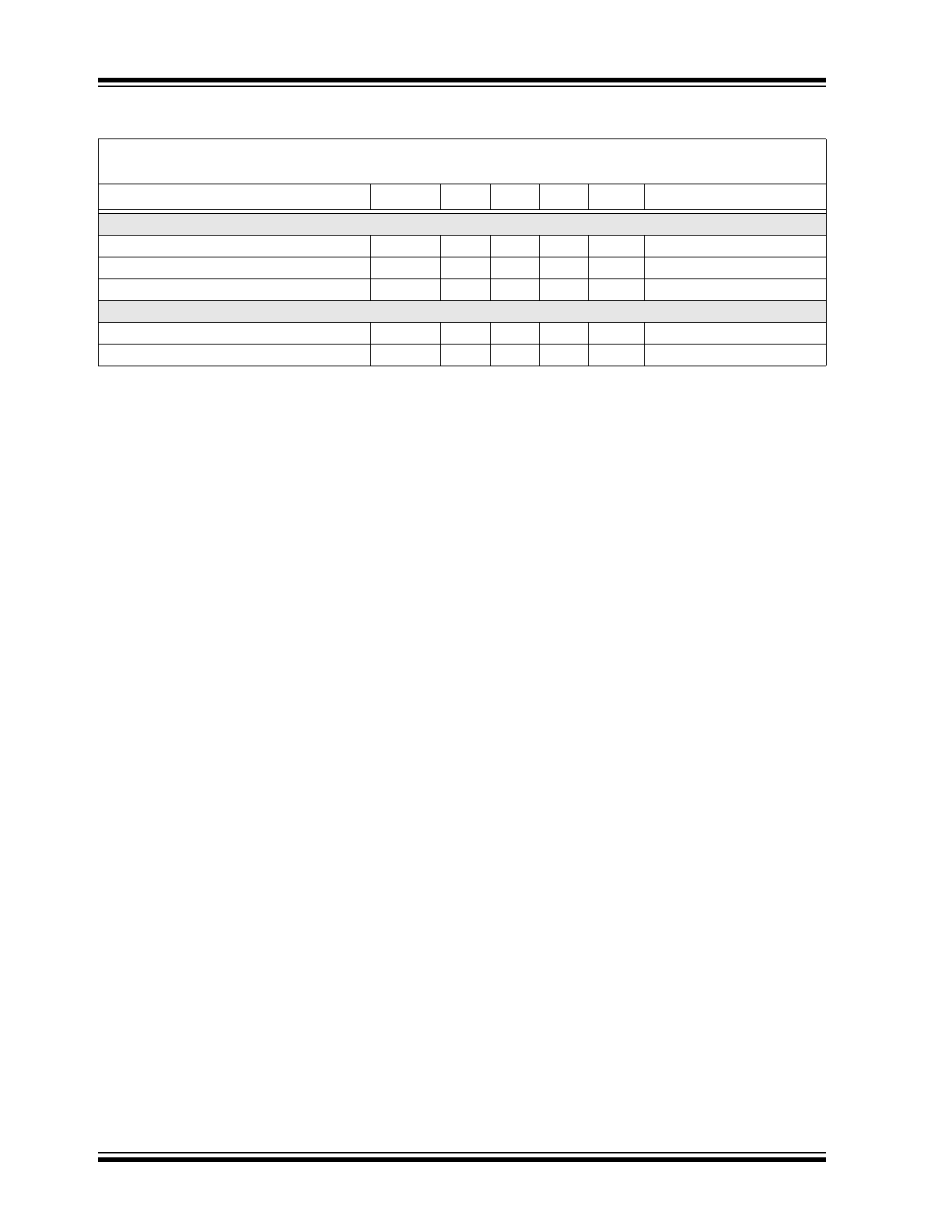
TEMPERATURE CHARACTERISTICS
Electrical Specifications:
Unless otherwise indicated, V
DD
= 9V, Typical Application (unless otherwise noted),
V
SS
= 0V
Parameters
Sym.
Min.
Typ.
Max.
Units
Conditions
Temperature Ranges
Specified Temperature Range
T
A
-25
—
+75
°C
Operating Temperature Range
T
A
-25
—
+75
°C
Storage Temperature Range
T
STG
-55
—
+125
°C
Thermal Package Resistances
Thermal Resistance, 16L-PDIP
θJ
A
—
70
—
°C/W
Thermal Resistance, 16L-SOIC (150 mil)
θJ
A
—
86.1
—
°C/W