
2009-2014 Microchip Technology Inc.
DS20002166B-page 1
RE46C100
Features:
• Low Quiescent Current (< 100 nA)
• Low Driver R
ON
– 20
typical at 9V
• Wide Operating Voltage Range
• Available in 8-pin DFN, PDIP and SOIC packages
General Description:
The RE46C100 devices are intended for applications
using a self oscillating piezoelectric horn, although it
can be used in direct drive applications. Feedback
control and a driver circuit are provided, as well as a
horn enable function.
The RE46C100 is intended for use in smoke detectors,
CO detectors, personal security products and
electronic toys.
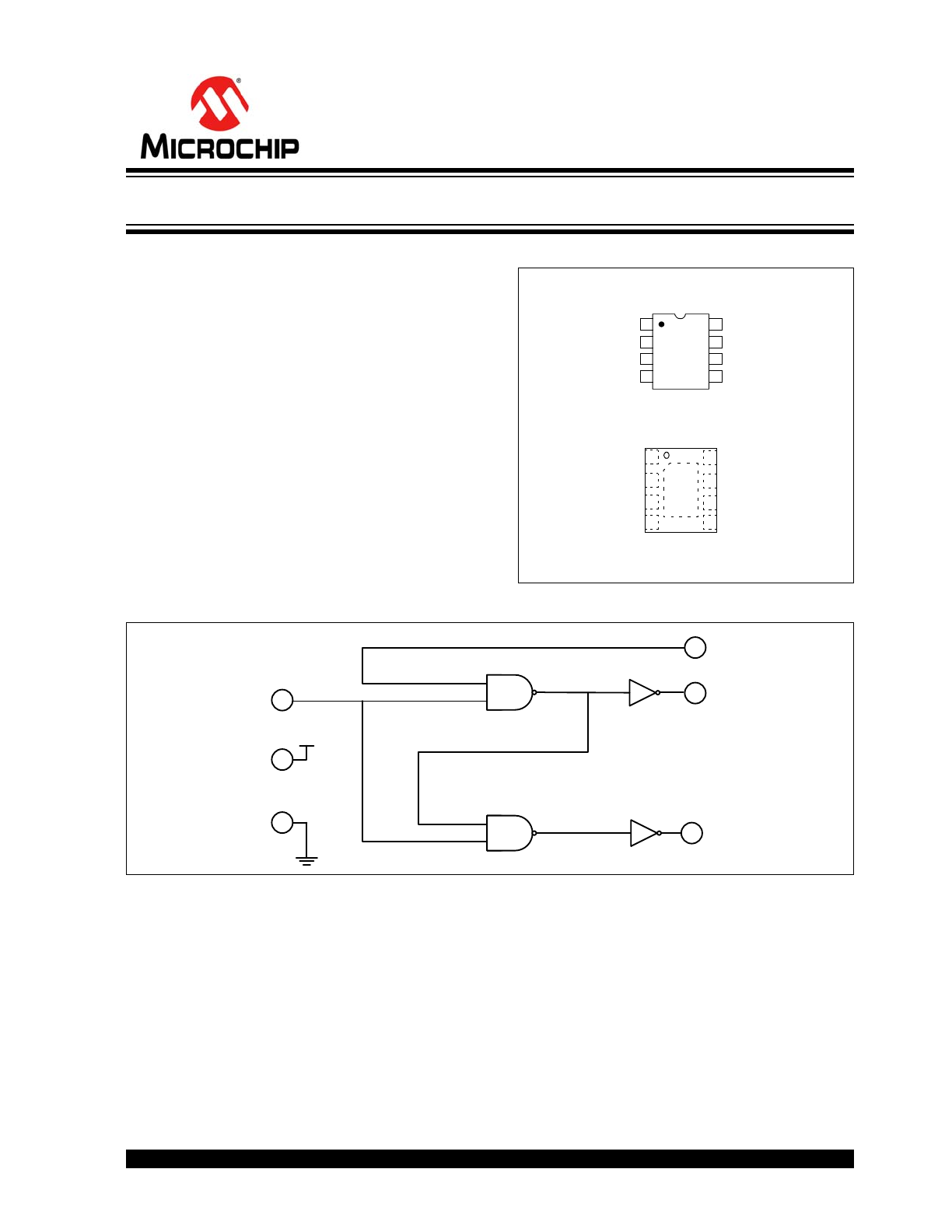
Package Types
Functional Block Diagram
HRNEN
5
6
7
8
HORNS
V
SS
HORNB
1
2
3
4
NC
NC
FEED
V
DD
RE46C100
PDIP, SOIC
RE46C100
2x3 DFN*
*
Includes Exposed Thermal Pad (EP); see
Table 2-1
.
NC
V
DD
FEED
HORNS
HORNB
1
2
3
4
8
7
6
5 V
SS
HRNEN
NC
EP
9
8
2
5
6
4
7
HRNEN
V
DD
V
SS
FEED
HORNS
HORNB
Piezoelectric Horn Driver Circuit
RE46C100
DS20002166B-page 2
2009-2014 Microchip Technology Inc.
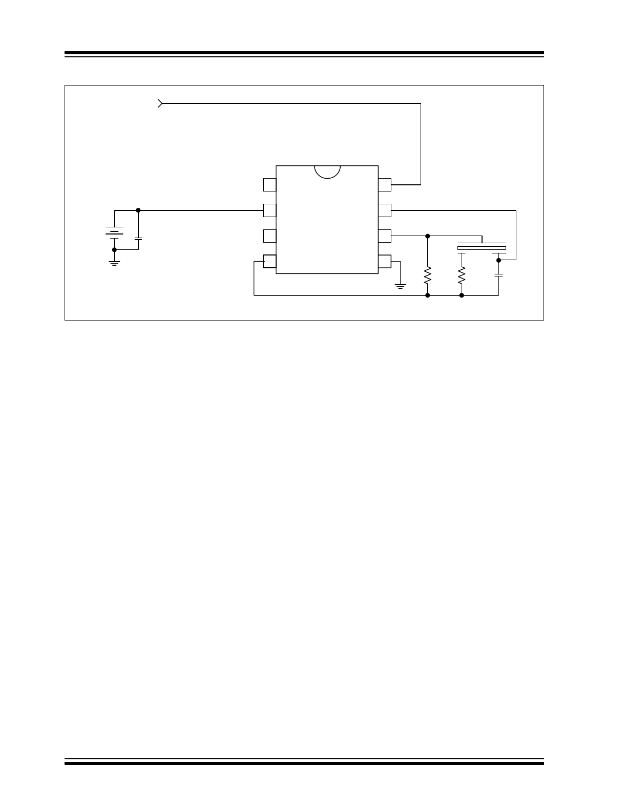
Typical Application
1
2
3
4
8
7
6
5
RE46C100
Horn Enable
Active High
9V
Battery
+
-
C2
(1)
1 µF
R3
1.5 MΩ
R4
220 kΩ
C1
0.001 µF
Note 1:
Place C2 close to the device power pins to minimize horn switching noise.
2009-2014 Microchip Technology Inc.
DS20002166B-page 3
RE46C100
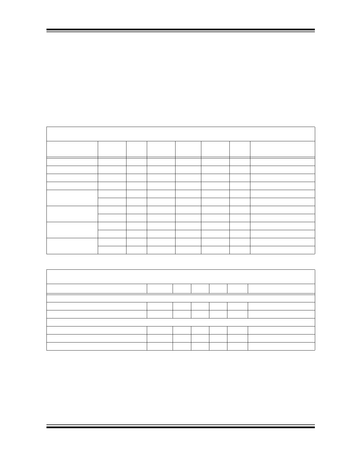
1.0
ELECTRICAL
CHARACTERISTICS
Absolute Maximum Ratings†
Supply Voltage.............................................................. V
DD
= 18V
Input Voltage Range Except FEED, TEST....... V
IN
= -0.3V to V
DD
+ 0.3V
FEED Input Voltage Range ........................... V
INFD
=-10 to +22V
Input Current except FEED .........................................I
IN
= 10 mA
Operating Temperature......................................T
A
= -40 to +85°C
Storage Temperature ...................................T
STG
= -55 to +125°C
Maximum Junction Temperature ............................... T
J
= +150°C
† Notice:
Stresses above those listed under “Maximum
ratings” may cause permanent damage to the device.
This is a stress rating only and functional operation of
the device at these or any other conditions above those
indicated in the operation listings of this specification is
not implied. Exposure to maximum rating conditions for
extended periods may affect device reliability.
DC ELECTRICAL CHARACTERISTICS
DC Electrical Characteristics:
Unless otherwise indicated, all parameters apply at T
A
= +25°C, V
DD
= 9V,
Typical Application.
Parameter
Symbol
Test
Pin
Min.
Typ.
Max.
Units
Conditions
Supply Voltage
V
DD
2
6
9
16
V
Operating
Supply Current
I
DD1
2
—
—
100
nA
HRNEN = 0V, FEED = 0V
Input Voltage Low
V
IL1
8
—
—
1
V
Input Voltage High
V
IH1
8
2.3
—
—
V
Input Leakage Low
I
IL1
8
—
—
-100
nA
V
IN
= V
SS
I
LFD
4
—
—
-50
µA
FEED = -10V
Input Leakage High
I
IH1
8
—
—
100
nA
V
IN
= V
DD
I
HFD
4
—
—
50
µA
FEED = 22V
Output Voltage Low
V
OL1
6, 7
—
0.3
0.5
V
I
OL
= 16 mA
V
OL2
6, 7
—
—
0.9
V
I
OL
= 16 mA, V
DD
= 7.2V
Output Voltage High
V
OH1
6, 7
8.5
8.7
—
V
I
OH
= -16 mA
V
OH2
6, 7
6.3
—
—
V
I
OH
= -16 mA, V
DD
= 7.2V
TEMPERATURE SPECIFICATIONS
Electrical Specifications:
Unless otherwise indicated, all parameters apply at T
A
= +25°C, V
DD
= 9V,
Typical Application.
Parameters
Sym.
Min.
Typ.
Max.
Units
Conditions
Temperature Ranges
Operating Temperature Range
T
A
-40
—
+85
°C
Storage Temperature Range
T
STG
-55
—
+125
°C
Thermal Package Resistances
Thermal Resistance, 8L 2x3 DFN
θ
JA
—
75
—
°C/W
Thermal Resistance, 8L-PDIP
θ
JA
—
89.3
—
°C/W
Thermal Resistance, 8L-SOIC
θ
JA
—
149.5
—
°C/W
RE46C100
DS20002166B-page 4
2009-2014 Microchip Technology Inc.
2.0
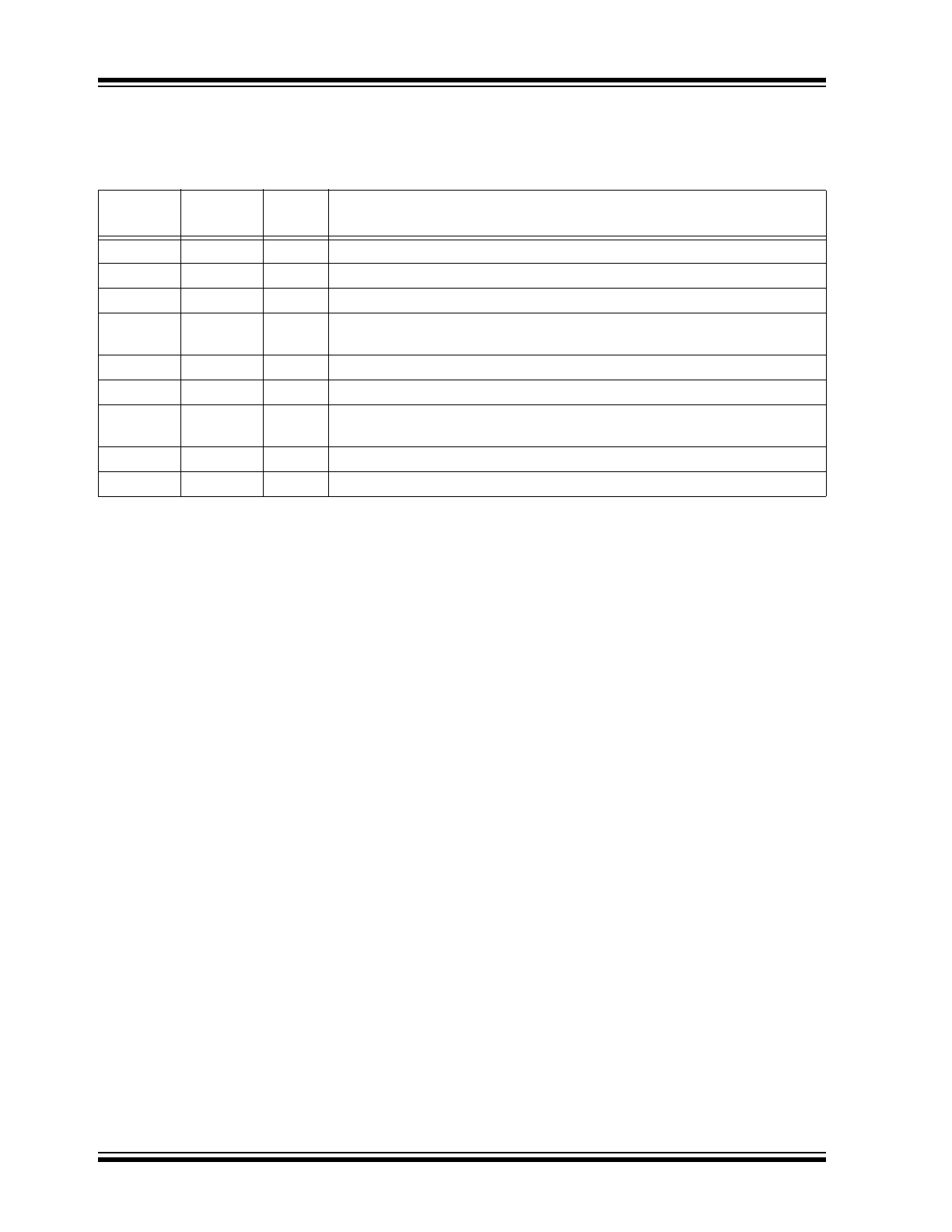
PIN DESCRIPTIONS
The descriptions of the pins are listed in
Table 2-1
.
TABLE 2-1:
PIN FUNCTION TABLE
RE46C100
PDIP, SOIC
RE46C100
DFN
Symbol
Description
1
1
NC
No connection
2
2
V
DD
Connect to the positive supply voltage
3
3
NC
No connection
4
4
FEED
Usually connected to the feedback electrode through a current-limiting resistor.
If not used, this pin must be connected to V
DD
or V
SS
.
5
5
V
SS
Connect to the negative supply voltage
6
6
HORNB This pin is connected to the metal electrode of a piezoelectric transducer.
7
7
HORNS This pin is a complementary output to HORNB, connected to the ceramic
electrode of the piezoelectric transducer.
8
8
HRNEN This pin enables the horn with a logic high.
—
9
EP
Exposed thermal pad. This pad should be connected to V
SS
.

2009-2014 Microchip Technology Inc.
DS20002166B-page 5
RE46C100
3.0
DEVICE DESCRIPTION
The RE46C100 horn driver provides the circuitry
necessary to drive a three-terminal self-oscillating
piezoelectric horn. It can also drive a two-terminal
piezoelectric horn with the FEED pin used as a signal
input. The horn driver provides a push-pull circuit to
drive the horn, as shown in the
Typical Application
circuit.
In a self-oscillating application, the FEED pin is
connected to the feedback pin of the piezoelectric horn
through a resistor. To drive a two-terminal piezoelectric
horn with an external signal, the FEED pin should be
used as the external signal input. The horn is enabled
when HRNEN is driven to a logic high and is silenced
when HRNEN is driven to a logic low. The horn output
can be modulated using the HRNEN input.
RE46C100
DS20002166B-page 6
2009-2014 Microchip Technology Inc.
4.0
PACKAGING INFORMATION
4.1
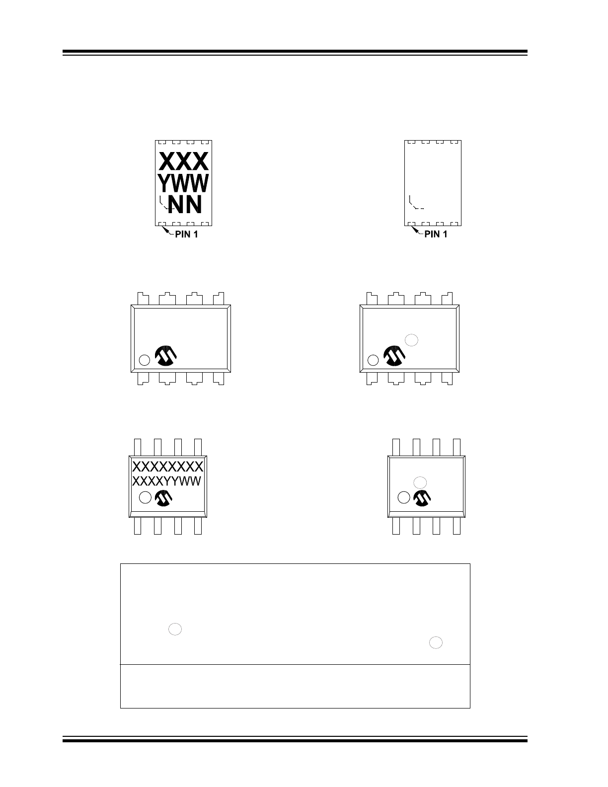
Package Marking Information
XXXXXXXX
XXXXXNNN
YYWW
8-Lead DFN (2x3x0.9 mm)
Example
ADG
420
25
8-Lead PDIP (300 mil)
Example
RE46C100
I/P^^^256
1420
Legend:
XX...X
Customer-specific information
Y
Year code (last digit of calendar year)
YY
Year code (last 2 digits of calendar year)
WW
Week code (week of January 1 is week ‘01’)
NNN
Alphanumeric traceability code
Pb-free JEDEC designator for Matte Tin (Sn)
*
This package is Pb-free. The Pb-free JEDEC designator ( )
can be found on the outer packaging for this package.
Note
:
In the event the full Microchip part number cannot be marked on one line, it will
be carried over to the next line, thus limiting the number of available
characters for customer-specific information.
3
e
3
e
3
e
8-Lead SOIC (3.90 mm)
Example
NNN
46C100I
SN^^^1420
256
3
e
2009-2014 Microchip Technology Inc.
DS20002166B-page 7
RE46C100
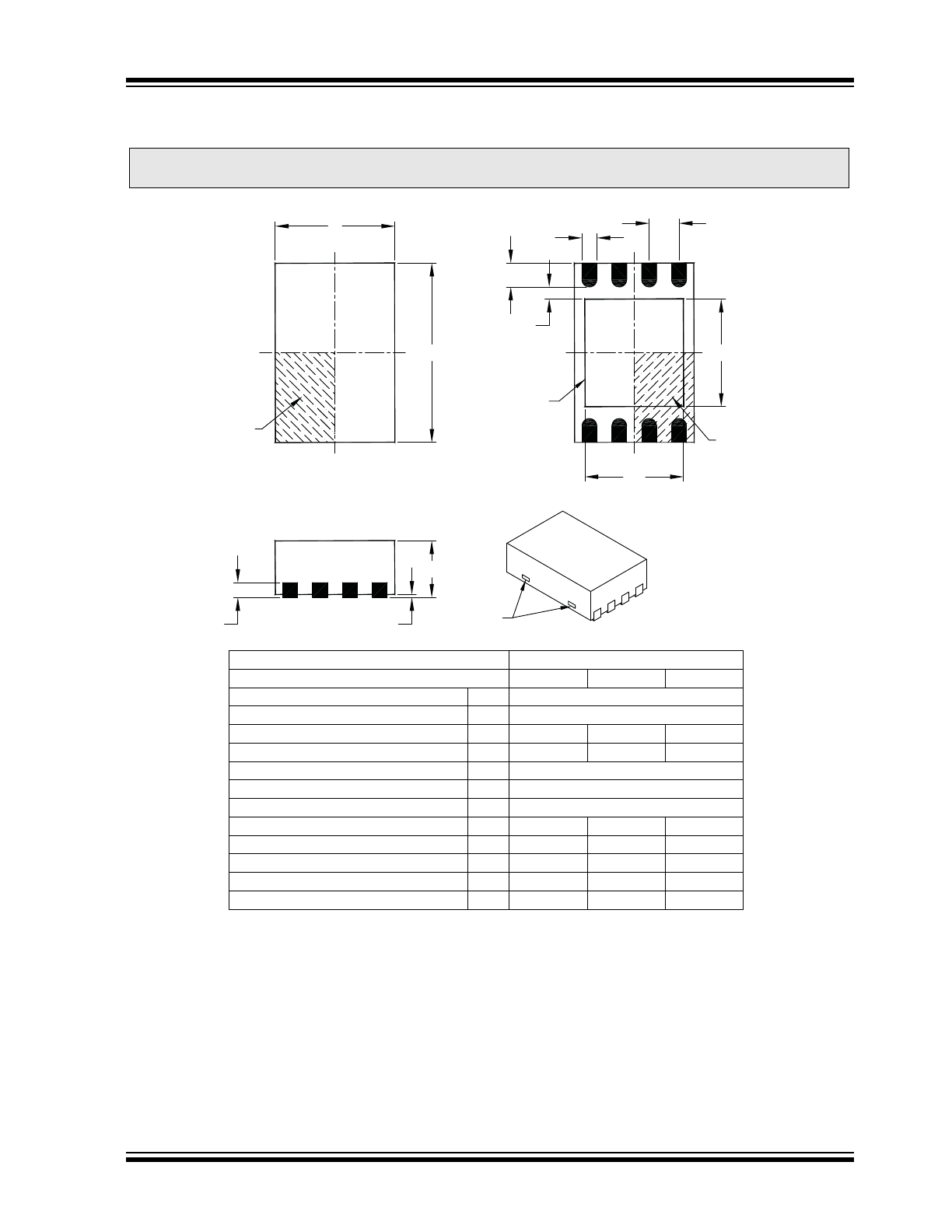
!""#$%&
'
!"#$%&"' ()"&'"!&)&#*&&&#
+
' '$!#&)!&#!
, + !!*! "&#
'! #& -./
012 0!'!&$& "!**&"&&!
-32 %'!("!"*&"&&(%%'&"!!
'
3&'!&"&+
#*
!(!!&+
%&&#&
&&244***''4+
5&!
66--
'!6'&!
7
78
9
7"')%!
7
:
&
/01
8 ; &
:
&#%%
/
1&&+!!
,
-3
8 6 &
01
8 <#&
-
,01
-$!##6 &
,
=
//
-$!##<#&
-
/
=
/
1&&<#&
)
/
,
1&&6 &
6
,
/
1&& & -$!##
>
=
=
D
N
E
NOTE 1
1
2
EXPOSED PAD
NOTE 1
2
1
D2
K
L
E2
N
e
b
A3
A1
A
NOTE 2
BOTTOM VIEW
TOP VIEW
* 1 ,1
RE46C100
DS20002166B-page 8
2009-2014 Microchip Technology Inc.
Note:
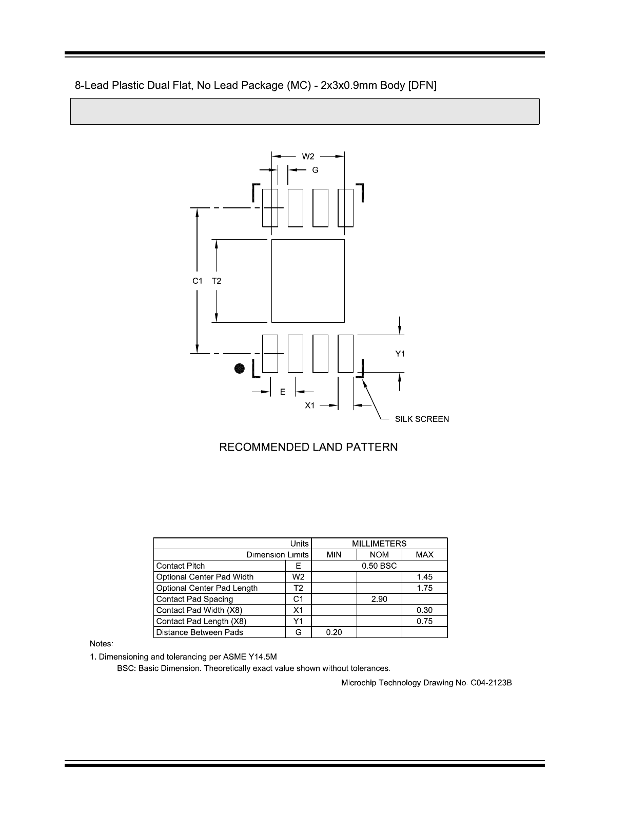
For the most current package drawings, please see the Microchip Packaging Specification located at
http://www.microchip.com/packaging
2009-2014 Microchip Technology Inc.
DS20002166B-page 9
RE46C100
B
A
For the most current package drawings, please see the Microchip Packaging Specification located at
http://www.microchip.com/packaging
Note:
Microchip Technology Drawing No. C04-018D Sheet 1 of 2
8-Lead Plastic Dual In-Line (P) - 300 mil Body [PDIP]
eB
E
A
A1
A2
L
8X b
8X b1
D
E1
c
C
PLANE
.010
C
1
2
N
NOTE 1
TOP VIEW
END VIEW
SIDE VIEW
e
RE46C100
DS20002166B-page 10
2009-2014 Microchip Technology Inc.
Microchip Technology Drawing No. C04-018D Sheet 2 of 2
For the most current package drawings, please see the Microchip Packaging Specification located at
http://www.microchip.com/packaging
Note:
8-Lead Plastic Dual In-Line (P) - 300 mil Body [PDIP]
Units
INCHES
Dimension Limits
MIN
NOM
MAX
Number of Pins
N
8
Pitch
e
.100 BSC
Top to Seating Plane
A
-
-
.210
Molded Package Thickness
A2
.115
.130
.195
Base to Seating Plane
A1
.015
Shoulder to Shoulder Width
E
.290
.310
.325
Molded Package Width
E1
.240
.250
.280
Overall Length
D
.348
.365
.400
Tip to Seating Plane
L
.115
.130
.150
Lead Thickness
c
.008
.010
.015
Upper Lead Width
b1
.040
.060
.070
Lower Lead Width
b
.014
.018
.022
Overall Row Spacing
eB
-
-
.430
BSC: Basic Dimension. Theoretically exact value shown without tolerances.
3.
1.
protrusions shall not exceed .010" per side.
2.
4.
Notes:
§
-
-
Dimensions D and E1 do not include mold flash or protrusions. Mold flash or
Pin 1 visual index feature may vary, but must be located within the hatched area.
§ Significant Characteristic
Dimensioning and tolerancing per ASME Y14.5M
e
DATUM A
DATUM A
e
b
e
2
b
e
2
ALTERNATE LEAD DESIGN
(VENDOR DEPENDENT)