
© 2006 Microchip Technology Inc.
DS21904C-page 1
PS810
H
ardware Features
• Highly accurate fuel gauge for single cell Li Ion
applications
• Algorithms are implemented using an embedded
PIC18 low-power microcontroller with 16-bit
instruction set
• Reports current, voltage and temperature utilizing a
programmable 8 to15-bit + sign, sigma-delta ADC
• Host communication accomplished through an
industry standard SMBus interface or an
alternative single pin serial interface
• I/O pins are available to provide functions such as
digital GPIO, coin cell voltage measurement and
thermistor input
• Integrated temperature sensor and regulator
minimize external components
• Embedded fuel gauge algorithms and application
specific parameters are stored in a 4K x 16 Flash
memory
• 512 bytes of RAM are available for temporary
storage of battery parameters
Software Features
• Provides battery status, such as average time to empty,
relative State-Of-Charge and battery State-Of-Health
• In-system offset calibration compensates for
offset error in current measurement
Package Features
• 16-pin QFN package or 14-pin TSSOP package
• -20°C to +85°C operating temperature range
Pin Description
1.0
PRODUCT OVERVIEW
The PS810 is a fuel gauge for one-cell Li Ion or Li Poly-
mer applications. The device provides the host and the
system user with critical battery information, such as
voltage, current, temperature, run time, State-Of-Charge
and State-Of-Health. This information is available
through an industry standard SMBus or an alternative
Single Pin Serial interface. Advanced fuel gauge
algorithms are stored in on-board Flash memory and
executed by the industry recognized PIC18 micro-
controller. These algorithms include compensation
factors which optimize the performance of the battery for
a specific application and operating environment.
Compensation is included for the effects of temperature,
discharge rate, charge rate and battery aging.
To provide precise measurements of current, voltage and
temperature, the PS810 integrates a highly accurate
15-bit + sign, sigma-delta A/D converter. Based upon
operating conditions, this programmable converter can be
configured to measure specific battery parameters with a
resolution of 8 to 15 bits + sign. Precision measurements
combined with advanced algorithms provide accurate
indications of capacity, run time, State-Of-Health and
safety and charge/discharge conditions.
The ability to operate directly from a single Li Ion or Li
Polymer cell minimizes the need for external compo-
nents, such as a voltage regulator and voltage divider.
To further limit external circuitry and enhance accuracy,
the PS810 provides an integrated temperature sensor
and oscillator.
IO4
GND
N/C
VC1
IO1
NTC/IO2
1
2
3
4
5
6
7
16 15 14 13
12
11
10
PS810
8
9
IO5
R
OSC
16-pin QFN (4 mm x 4 mm)
V
COIN
/IO3
V
FILTER
MCLR
N/C
S
C
L/IO
0
IO6
SDA/
SP
S
SR
2
NTC/IO2
SDA/SPS
GND
SR
MCLR
VC1
IO6
IO5
V
COIN
/IO3
V
FILTER
1
2
3
4
5
6
7
14
13
12
11
10
9
8
PS810
IO4
R
OSC
SCL/IO0
IO1
14-pin TSSOP
Li Ion Single Cell Fuel Gauge
PS810
DS21904C-page 2
© 2006 Microchip Technology Inc.
TABLE 1-1:
PS810 QFN PIN SUMMARY
TABLE 1-2:
PS810 TSSOP PIN SUMMARY
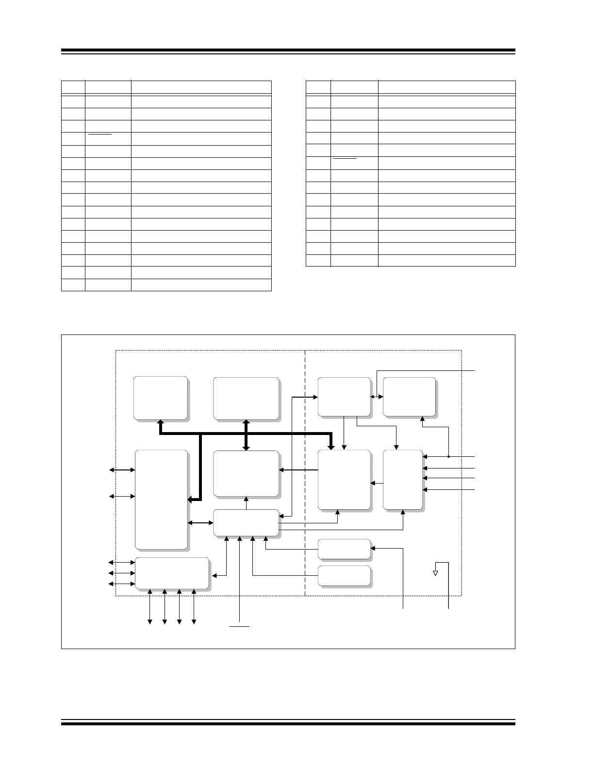
FIGURE 1-1:
PS810 INTERNAL BLOCK DIAGRAM
Pin#
Pin Name
Description
1
NTC/IO2
External NTC input or GPIO
2
V
COIN
/IO3
Coin cell monitor input or GPIO
3
V
FILTER
Power supply filter cap
4
MCLR
Master Clear
5
VC1
Cell voltage input
6
N/C
No connect
7
N/C
No connect
8
R
OSC
Oscillator bias resistor
9
SR
Sense resistor input
10
GND
Power supply ground
11
IO4
General purpose IO
12
IO5
General purpose IO
13
IO6
General purpose IO
14
SDA/SPS
SMBus data/one-wire serial line
15
SCL/IO0
SMBus clock or GPIO0
16
IO1
General purpose IO
Pin#
Pin Name
Description
1
SCL/IO0
SMBus clock or GPIO
2
IO1
General purpose IO
3
NTC/IO2
External NTC input or GPIO
4
V
COIN
/IO3
Coin cell monitor input or GPIO
5
V
FILTER
Power supply filter cap
6
MCLR
Master Clear
7
VC1
Cell voltage input
8
R
OSC
Oscillator bias resistor
9
SR
Sense resistor input
10
GND
Power supply ground
11
IO4
General purpose IO
12
IO5
General purpose IO
13
IO6
General purpose IO
14
SDA/SPS
SMBus data/one-wire serial line
4K x 16 Flash
4K x 16 Flash
512-byte RAM/
Registers
512-byte RAM/
Registers
Voltage
Reference and
Temp Sensor
Voltage
Reference and
Temp Sensor
Voltage
Regulator
Voltage
Regulator
Comm
Interface
Comm
Interface
PIC18F
Microcontroller
PIC18F
Microcontroller
15-bit + sign
Sigma-Delta
Integrating
A/D Converter
15-bit + sign
Sigma-Delta
Integrating
A/D Converter
Analog
Input Mux
Analog
Input Mux
Run
Oscillator
Run
Oscillator
VC1
R
OSC
GND
Digital Section
Analog Section
Control and Status
Control and Status
SCL
V
COIN
SDA/SPS
Sleep
Oscillator
Sleep
Oscillator
IO0
Input/Output
Input/Output
NTC
SR
IO1
IO2
IO5
IO4
IO3
IO6
MCLR
V
FILTER
© 2006 Microchip Technology Inc.
DS21904C-page 3
PS810
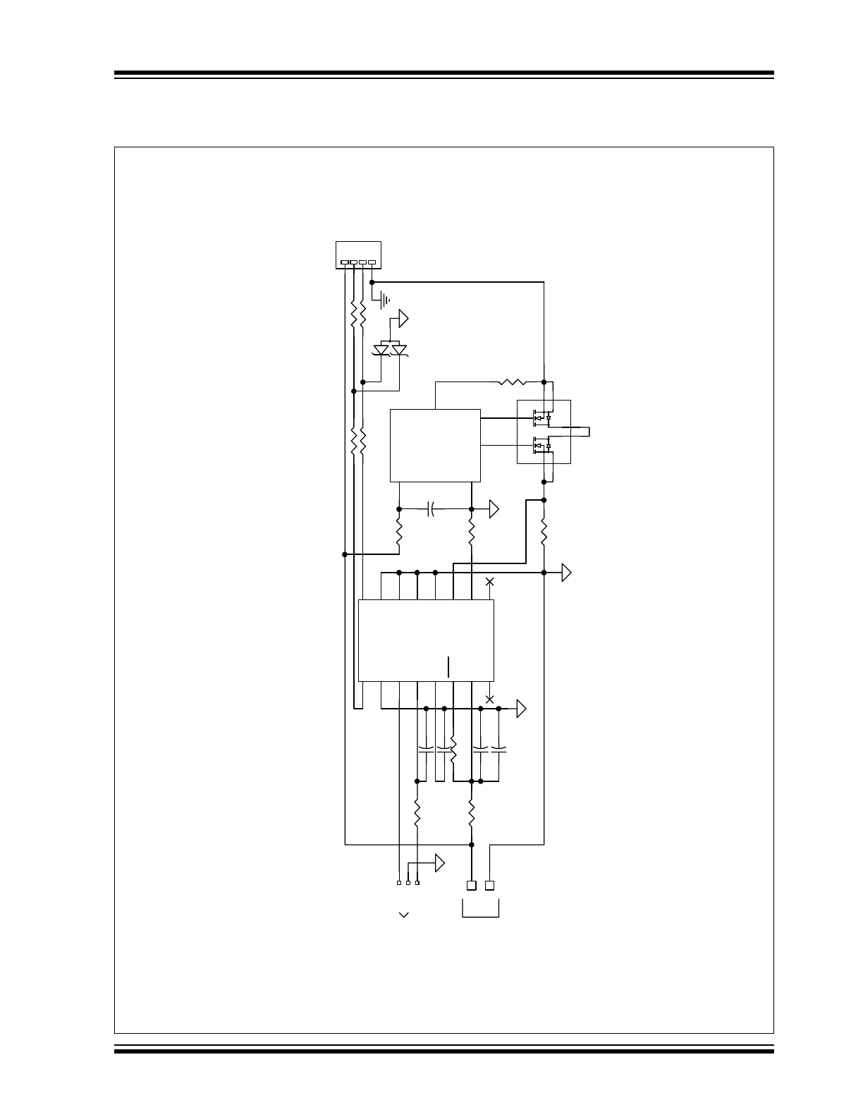
1.1
Schematic
FIGURE 1-2:
PS810 APPLICATION SCHEMATIC – PS810-BASED BATTERY PACK
R3
1
1.
0K
R8
232K
R2
1
240
R2
0
240
PACK CONNECTI
ON
R9
0.
020
3
1
2
D1
CMSZDA5
V6
CONNECTI
ON
GROUND PLANE
C1
0
1.
0 nF
3
4
2
1
5
6
8
7
Q1
TPC
S8209
R5
20
C5 100 nF
R
4
20K
CEL
L CONNECTI
ONS
R1
5
20
R1
4
20
V1
VR
B+ C D B-
QFN PACKAGE
VC1
5
V
COIN
/IO3
2
NTC/IO2
1
SR
9
GND
10
SCL/IO0
15
SDA/SPS
14
R
OSC
8
IO1
16
IO4
11
IO6
13
V
FILTER
3
MCLR
4
IO5
12
NC
6
NC
7
U1
PS810Q
R3
2
470
C3
2
100 nF
V
DD
2
V
SS
3
VM
1
CO
5
DO
4
U
2
S8241A
SAFETY
IC
NTC NVR V
COIN
R2
240
C3 100 nF
C2 100 nF
EXT.
THERMI
STOR I
N
PUT
COI
N CELL
IN
PUT
* GROUND I
F NOT USED
*
*

PS810
DS21904C-page 4
© 2006 Microchip Technology Inc.
1.2
Bill of Materials
TABLE 1-3:
PS810 BILL OF MATERIALS
ID
Part Number
Symbol
Description
Mftr.
Mftr. PN
Supplier
Supplier PN
Qty
1
04-826197 Rev. 1.1
Raw PCB, PS8110
Microchip
04-826197 Rev. 1.1
Microchip
04-826197 Rev. 1.1
1
2
CC-0402-10X7R25-1.0NF-01
C10
Capacitor, Ceramic, 1.0 nF,
25V, +/-10%, X7R dielectric,
0402
Panasonic
ECJ-0EB1E102K
Digikey
PCC102BQCT-ND
1
3
CC-0603-10X7R16-100NF-01
C2, C3,
C5, C32
Capacitor, Ceramic, 100 nF,
16V, +/-10%, X7R dielectric,
0603
Panasonic
ECJ-1VB1C104K
Digikey
PCC1762CT-ND
4
4
DZ-SOT323-10D-CMSZDA5V6-01 D1
Dual Zener Diode, 5.6V,
+/-10%, 200 mW,
common anode, SOT-323
Central Semi.
Diodes Inc.
CMSZDA5V6
AZ23C5V6W-7
Central Semi.
Diodes Inc.
CMSZDA5V6
AZ23C5V6W-7
1
5
QM-TSSOP844-DN-TPCS8209-01 Q1
MOSFET, dual N-channel
Enhancement mode, 20V,
5A, TSSOP-8/4.4 mm body
width package
Toshiba
TPCS8209(TE12L)
Digikey
TPCS8209CT-ND
1
6
RF-0402-5-20-01 (Note 1)
R14, R15
Resistor, film, 0402, 5%,
20 ohms
Panasonic
ERJ-2GEJ200X
Digikey
P20JCT-ND
2
7
RF-0402-5-20K-01 (Note 1)
R4
Resistor, film, 0402, 5%,
20 kOhms
Panasonic
ERJ-2GEJ203X
Digikey
P20KJCT-ND
1
8
RF-0603-ITC25-221K-01 (Note 1)
R8
Resistor, film, 0603, 1%,
232 kOhms, 25 ppm TC
Susumu Co.
Ltd.
RR0816P-2213-D-34D
Digikey
RR08P221KDCT-ND
1
9
RF-0603-5-1.0K-01 (Note 1)
R31
Resistor, film, 0603, 5%,
1.0 kOhms
Panasonic
ERJ-3GEYJ102V
Digikey
P1.0KGCT-ND
1
10 RF-0603-5-470-01 (Note 1)
R32
Resistor, film, 0603, 5%,
470 ohms
Panasonic
ERJ-3GEYJ471V
Digikey
P470GCT-ND
1
11 RF-0805-5-20-01 (Note 1)
R5
Resistor, film, 0805, 5%,
20 ohms
Panasonic
ERJ-6GEYJ200V
Digikey
P20ACT-ND
1
12 RF-0805-5-240-01 (Note 1)
R2, R20,
R21
Resistor, film, 0805, 5%,
240 ohms
Panasonic
ERJ-6GEYJ241V
Digikey
P240ACT-ND
3
13 RF-1206-1-0.029-01 (Note 1)
R9
Resistor, metal strip, 1206,
1%, 0.020 ohms
Vishay
WSL1206-0.020-1%-R86 Vishay
WSL1206-0.020-1%-R86
1
14 UM-SOT235-4085-
S8241ABPMCGBPT2-01
U2
IC, Battery Protection Circuit,
Li Ion, 1-cell, -40°C to +85°C,
SOT23-5 package
Seiko
Instruments
S-8241ABPMC-GBP-T2
(Note 2)
Seiko
Instruments
S-8241ABPMC-GBP-T2
(Note 2)
1
15 UM-QFN164X4-2085-PS810-01
U1
IC, Low-Voltage Fuel Gauge,
-20°C to +85°C, QFN-16/
4.0x4.0 mm package
Microchip
PS810
Microchip
PS810
1
Note
1:
Resistor sizes shown are minimum recommended sizes for the application.
2:
Other variants of the S-8241A series, with different trip points, are also available. Consult the S-8241A series data sheet.

© 2006 Microchip Technology Inc.
DS21904C-page 5
PS810
2.0
ARCHITECTURAL OVERVIEW
The PS810 contains a complete analog “front-end” for
battery monitoring as well as an embedded micro-
controller, with supporting memory, for control,
measurement accumulation, calculation and
communications. Major functions within the PS810
include:
• Voltage Regulator
• Precision Time Base
• Temperature Sensor
• 4K x 16 Flash Memory
• 512-byte RAM Memory
• 15-bit plus sign Analog-to-Digital (A/D) Converter
• SMBus/I
2
C™ or Single Pin Serial
Communications Interface
• PIC18 Microcontroller
Figure 1-1 is a block diagram of the internal circuitry of
the PS810. Figure 1-2 is a schematic diagram that
depicts the PS810 in a typical single cell lithium ion
application. The function of each of the blocks listed
above is summarized in the following sections.
2.1
Internal Voltage Regulator
The PS810 incorporates an internal voltage regulator
that supports 1-cell lithium pack configurations. The
internal regulator draws power directly from the VC1
input. No other external components are required to
regulate circuit voltage.
2.2
Precision Time Base
The integrated precision time base is a highly accurate
RC oscillator that provides precise timing for the sigma-
delta A/D and for the on-chip elapsed time counters
without the need for an external crystal. This time base
is trimmed during manufacturing to a nominal
frequency of 512 kHz.
2.3
Temperature Sensor
An integrated temperature sensor is provided that can
eliminate the need for an external thermistor. As an
option, a connection is provided for an external
thermistor for applications where the battery cell is
physically separated from the PS810.
2.4
Flash Memory
4K x 16 of Flash memory is incorporated for storage of
nonvolatile parameters, such as PowerSmart
®
3D cell
models, fuel gauge algorithms and application specific
data.
2.5
RAM Memory
512 bytes of general purpose RAM memory is provided
for storage of temporary parameters.
2.6
A/D Converter
The PS810 incorporates an integrating sigma-delta
A/D converter together with an analog that has inputs
for charge and discharge current, cell voltage, coin cell
voltage, the on-chip temperature sensor and an off-chip
thermistor. The converter can be programmed to per-
form a conversion with resolutions of 8 to 15 bits + sign,
while utilizing either a single-ended +300 mV or a
differential ±150 mV reference.
2.7
SMBus/I
2
C™ or Single Pin Serial
Communications Interface
This communications port for the PS810 is selectable
as a 2-pin industry standard SMBus/I
2
C or a single pin
interface. All commands, status and data are read or
written from the host system via this interface.
2.7.1
SMBus/I
2
C
The two pin communication interface uses one clock
pin and one data pin and is compatible with the industry
standard System Management Bus (SMBus) and the
Inter IC Communication Bus (I
2
C).
2.7.2
SINGLE PIN SERIAL INTERFACE
The Single Pin Serial (SPS) interface consists of one pin
only: the SDA/SPS pin (pin 14). This communication is
an asynchronous return-to-one protocol. The timing of
the driven low pulses defines the communication.
2.8
PIC18 Microcontroller
The PIC18 is a high-performance, CMOS, fully static
8-bit microcontroller. The PIC18 employs an advanced
RISC architecture. This device has enhanced core
features, such as 31 level deep stack and multiple
internal and external interrupt sources. The separate
instruction and data buses of the Harvard architecture
allow a 16-bit wide instruction word with a separate 8-bit
wide data bus. The two-stage instruction pipeline allows
all instructions to execute in a single cycle, except for
program branches, which require two cycles. A total of
75 instructions are available.

PS810
DS21904C-page 6
© 2006 Microchip Technology Inc.
NOTES:

© 2006 Microchip Technology Inc.
DS21904C-page 7
PS810
3.0
OPERATIONAL DESCRIPTION
3.1
A/D Operation
The PS810 A/D converter measures current, voltage
and temperature and integrates the current over time to
calculate State-Of-Charge. Cell voltage is measured
with a direct connection to the battery cell without
requiring an external voltage divider. Using an external
sense resistor, current is monitored during both charge
and discharge and is integrated over time using the on-
chip oscillator as the time base. Temperature is
measured from the on-chip temperature sensor or an
optional external thermistor. Voltage, current and
temperature can be calibrated for accuracy over the
operational range. The A/D converter performs
sampling using a 32 kHz clock.
3.1.1
CURRENT MEASUREMENT
The A/D input channels for current measurement are the
SR and GND pins. The voltage drop across the sense
resistor is measured and converted mathematically into
a current measurement. The current is also integrated
over time to get the amount of charge entering or leaving
the battery.
A sense resistor is connected to SR and GND. The
maximum input voltage that can be measured at SR is
+/-150 mV. The sense resistor should be properly sized
to accommodate the lowest and highest expected
charge and discharge currents, including suspend and/
or standby currents.
The parameter NullCurr represents the zero-zone
current of the battery. This is provided as a calibration
guardband for reading zero current. Currents below
+/- NullCurr (in mA) limit are read as zero and not
included in the capacity algorithm calculations. A
typical value for NullCurr is 3 mA, therefore, currents
between -3 mA and +3 mA will be reported as zero and
not included in the capacity calculations. This feature is
provided so that electrical noise on the battery module
current path is not interpreted as actual charge entering
or leaving the battery.
3.1.1.1
Sense Resistor Selection and
Current Measurement Range
The current resolution is based on the smallest amount
of voltage the A/D converter can measure across the
sense resistor. Since this measurement uses 13 bits
(plus sign) and the reference used is the internal
150 mV reference, the smallest voltage across the
sense resistor that can be measured is:
EQUATION 3-1:
3.1.1.2
Current Calibration
In-circuit calibration of the current is done using the
communication interface (SMBus/I
2
C or SPS) at time
of manufacture to obtain optimal accuracy. A correction
is calculated and stored for both offset and slope.
COD is a constant that is measured at calibration time
and contains the offset due to external PCB
components.
CFCurr is the “Correction Factor for Current” which
compensates the A/D gain and any variances in the
actual sense resistance over varying currents. It is
multiplied against the raw A/D measurement.
COCurr is the “Correction Offset for Current” which is
updated in real time by the A/D shorting the inputs and
comparing any result to zero. This is added to COD and
compensates for any offset that varies over time, such
as temperature dependent offsets.
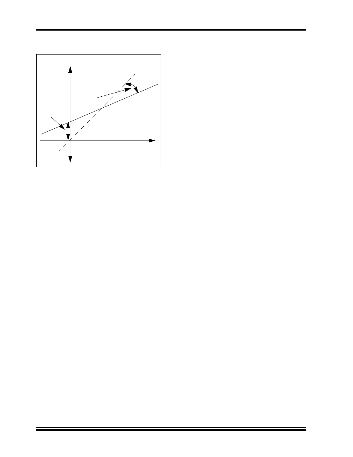
Figure 3-1 shows the relationship of the COCurr and
CFCurr values.
150 mV/(2 ^ 13
– 1) = 150 mV/32767 = 18.3
μV
Thus, the smallest current that can be measured is:
18.3
μV/R
SENSE
(m
Ω)
The largest current that can be measured is:
150 mV/R
SENSE
(m
Ω)
Example: a 20 milliohm sense resistor will measure
from:
18.3
μV/20 mΩ = 0.915 mA
(though will be recorded as zero if < NullCurr)
up to:
150 mV/20 m
Ω = 7.5 Amps
PS810
DS21904C-page 8
© 2006 Microchip Technology Inc.
FIGURE 3-1:
COCurr AND CFCurr
VALUE RELATIONSHIP
3.1.2
AUTO-OFFSET COMPENSATION
Accuracy drift is prevented using an automatic auto-
zero self-calibration method which zeros the current
measurement circuit periodically at a programmable
rate. This feature can correct for drift in temperature
during operation. The Auto-Offset Compensation
circuit works internally by disconnecting the RS input
and internally shorting it to GND to measure the zero
input offset. Furthermore, the calibration factor, COD,
contains the offset factor external to the IC, offset due
to the circuit board, system, etc. COD is added to the
internal offset calculated by the auto-offset cycle to
determine the full offset, COCurr.
3.1.3
VOLTAGE MEASUREMENTS
The A/D input channel for cell voltage measurement is
the VC1 pin. Measurements are taken each measure-
ment period when the A/D is active. The maximum
voltage at the VC1 pin is 5.5V, but voltages above 4.5V
are not suggested since this will saturate the A/D. The
cell voltage is measured with an integration method to
reduce any sudden spikes or fluctuations. The A/D
uses a default of 11-bit plus sign resolution for these
measurements.
The VC1 input circuit contains an internal resistive
divider to reduce the external voltage input to a range
that the internal A/D circuit can accommodate (300 mV
maximum). The divider is 15 to 1 based on a maximum
cell voltage of 4.5 volts. The voltage divider is only
connected to ground when the actual voltage
measurement is occurring.
CFVoltage is the “Correction Factor for Pack Voltage”
which compensates for any variance in the actual A/D
response versus an ideal A/D response over varying
voltage inputs. In-circuit calibration of the voltage is
done at the time of manufacture to obtain accuracy in
addition to high resolution. Cell voltage measurements
can be accurate to within ±20 mV.
3.1.4
TEMPERATURE MEASUREMENTS
The A/D can measure temperature from the internal
temperature sensor or an external thermistor
connected to the NTC pin. The A/D uses a default of
11-bit plus sign resolution for the temperature
measurements.
A standard 10 kOhms at 25°C Negative-Temperature-
Coefficient (NTC) device of the 103ETB type is
suggested for the optional external thermistor. One leg
of the NTC should be connected to the NTC pin and the
other to ground.
A linearization algorithm is used to convert the voltage
measurement seen at the NTC pin to a temperature
value. The external thermistor should be placed as
close as possible to the battery cells and should be
isolated from any other sources of heat that may affect
its operation.
Calibration of the temperature measurements involves
a correction factor and an offset exactly like the current
measurement. The internal temperature measurement
makes use of correction factor, CFTempI and offset,
COTempI, while the NTC pin for the optional external
thermistor makes use of correction factor, CFTempE.
Ideal A/D Response
Actual A/D
Response
CFCurr
COCurr
Raw Measurement
Actual Current

© 2006 Microchip Technology Inc.
DS21904C-page 9
PS810
TABLE 3-1:
A/D OPERATION PARAMETERS
Parameter
Name
# of
Bytes
Units
Typical
Value
Operational Description
NullCurr
1
mA
3
Zero zone control is built into the PS810 so that electrical noise
doesn’t actually drain the gas gauge, when in fact the current is
zero. For this reason, current less than NullCurr mA in either
direction will be measured as zero.
CFCurr
2
unsigned
word
4200
Correction Factor for Current. Adjusts the scaling of the sense
resistor current measurements.
COCurr
1
signed
byte
0
Correction Offset for Current. This is the value the A/D reads
when zero current is flowing through the sense resistor.
COD
1
signed
byte
0
Correction Offset Deviation. Offset value for the auto-zero
calibration of the current readings.
AOMInterval
1
op cycles
60
Interval of time between auto-offset calibrations.
AVGIScale
1
coded
b00100000 Time period over which current is averaged to calculate
average current: I
AVG
= I
AVG
+ (I – I
AVG
)/(AVGIScale * 2).
Note: Only Most Significant set bit is used, others are ignored.
CFVoltage
2
integer
2250
Correction Factor for Pack Voltage. Adjusts the scaling of the
VC1 pin measurement.
CFCoin
2
integer
2250
Correction Factor for Coin Cell Measurement. Adjusts the
scaling of the V
COIN
pin measurement.
CFTempE
2
integer
326
Correction Factor for Temperature. Adjusts the scaling of
temperature measured across an external thermistor at the NTC
input pin.
CFTempI
2
integer
2038
Correction Factor for Temperature. Adjusts the scaling of
temperature measured from the internal temperature sensor.
COTempI
2
signed
word
21298
Correction Offset for Temperature. Used for temperature
measurement using internal temperature sensor.

PS810
DS21904C-page 10
© 2006 Microchip Technology Inc.
3.2
Operational Modes
The PS810 operates on a continuous cycle, measuring
current, voltage and temperature, then performing fuel
gauge calculations. There are four power modes: Run
mode, in which the measuring and calculating loop
constantly repeats; Bus Inactive Low-Power mode, in
which only self-discharge is calculated; Low-Voltage
Sleep mode, in which there are no measurements and
only wake-up circuitry is powered; and Shelf-Sleep
mode, in which only communication line sensors are
powered.
3.2.1
RUN MODE
Run mode is the highest power consuming mode.
During Run mode, all measurements and calculations
occur. Current, voltage and temperature measure-
ments are each made sequentially. Run mode is active
until voltage drops below the Sleep voltage, the bus
goes inactive or the Shelf-Sleep command is executed.
3.2.2
BUS INACTIVE LOW-POWER MODE
The PS810 enters Low-Power mode when all of the
following conditions are true:
• Current is zero (optional)
• The communication pins are low for at least
8 periods of 512 ms each
• There is no communication attempt for at least
8 periods of 512 ms each
To enter this mode, typically, there must be no load or
charger present and no communication host. The pack
is out of the system. In this mode, the PS810 will draw
less current from the battery, approximately 25
μA and
will only track self-discharge. Alternatively, if self-
discharge tracking is not required, Ultra Low-Power
mode can be used and the PS810 will draw less than
1 microamp.
3.2.3
LOW-VOLTAGE SLEEP MODE
Entry to Low-Voltage Sleep mode can only occur when
the measured pack voltage at VC1 input is below a
preset limit set by the parameter SleepVoltage (in mV)
and the current is zero (less than NullCurr). Sleep
mode may be exited to Run mode when the voltage at
VC1 is greater than the wake-up voltage, which is
3.2 volts, 10%.
While in 10% Sleep mode, no measurements occur
and no calculations are made. The fuel gauge display
is not operational, no communications are recognized
and only a wake-up condition will permit an exit from
Sleep mode. Sleep mode is one of the lowest power
consuming modes and is used to conserve battery
energy following a complete discharge.
There are two power levels that can be chosen for Low-
Voltage Sleep mode. Low-Power mode draws
approximately 20
μA and will wake-up automatically
when the voltage rises above the wake-up voltage,
which is a constant 3.2 volts above the wake-up volts,
+/-5%. Ultra Low-Power mode draws less than 1
μA
and requires an external source to drive the communi-
cation line high to wake-up, since the voltage wake-up
comparator is powered down.
3.2.4
SHELF-SLEEP MODE
Shelf-Sleep mode can be entered by a battery data
command on the communication bus for conserving
energy while shipping battery packs. It can be exited
only by an external source driving the communication
data line high. This mode uses the Ultra Low-Power
Sleep mode, resulting in current draw less than
1 microamp. This mode is entered by writing a pass-
word to SMBus command code, 0x43. A word write
protocol is used to write the password, 0x5A7A.
TABLE 3-2:
OPERATIONAL MODES
Mode
Entry
Exit
Notes
Run
Voltage > Wake-up voltage
or data line driven high
Voltage less than SleepVoltage, bus Idle or
Shelf-Sleep command issued
Highest power
consumption and
accuracy.
Bus Inactive
Low-Power
Current < NullCurr,
communication lines low
and no communication
attempts
Activity on communication lines
Only self-discharge
calculated.
Low-Voltage
Sleep
VC(1) < SleepVoltage,
Current is not zero
Voltage > Wake-up voltage (Low-Power mode),
Data line driven high (Ultra Low-Power mode)
No measurements
made.
Shelf-Sleep
Can be entered by SMBus
command
Data line driven high
No measurements
made.