
2004 Microchip Technology Inc.
DS21760F-page 1
PS700
Features
• Measures, maintains and reports all critical
rechargeable battery parameters with high
accuracy
• Supports Lithium (1-cell and 2-cell) battery packs
• Current measurement with 16-bit integrating A/D
accurate to less than ±0.5% error
• Temperature measurement accurate to within
±2°C absolute, using on-chip temperature sensor
or external thermistor
• Accumulation of charge current, discharge
current, temperature and voltage in independent
32-bit registers
• 512-byte nonvolatile EEPROM stores factory
programmed, measured and user-defined
parameters
• In-system offset calibration compensates for
offset error in current measurement
• Industry standard SMBus/I
2
C™ compatible 2-wire
communications interface
• 8-pin TSSOP package
• -20°C to +85°C operating temperature range
• NTC pin can be configured as a thermistor input
or GPIO
• VC2 pin can be configured as a cell input or a
GPIO
• Flexible power operating modes allow low-power
monitoring of battery conditions during system full
operating and standby conditions:
- Run: Continuous Conversion; 80
µ
A typ.
- Sample: Sample interval from
0.5-64s @ 45
µ
A typ.
- Sample-Sleep: Sample interval from
0.5-138s min. @ 20
µ
A typ.
• Shelf-Sleep mode reduces power consumption
during pack storage conditions to 300 nA typ.,
with automatic wake-up upon pack insertion
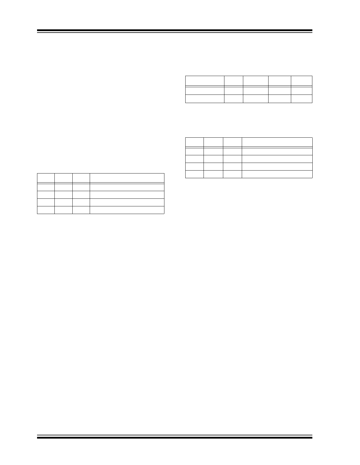
Pin Description
Pin Summary
Pin Name
Description
VC2/IO1
Cell voltage input for cell 2 in a
2-series Li Ion pack or general
purpose I/O #1
VC1
Cell voltage input for cell 1
SCL
SMBus clock line
SDA
SMBus data l/O
R
OSC
Oscillator bias resistor
NTC/IO0
External thermistor connection or
general purpose I/O #0
GND
Power supply ground
SR
Sense resistor input
R
OSC
PS700
1
SCL
2
3
GND
4
8
7
6
5
VC1
VC2/IO1
NTC/IO0
SR
SDA
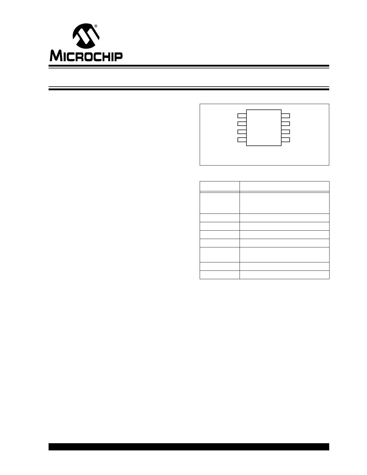
8-pin 150 mil
TSSOP Package
Battery Monitor
PS700
DS21760F-page 2
2004 Microchip Technology Inc.
1.0
PRODUCT OVERVIEW
The PS700 is a cost-effective, highly accurate IC that
measures, stores and reports all of the critical
parameters required for rechargeable battery monitor-
ing with a minimum of external components. It precisely
measures charge/discharge current as well as voltage
and temperature of a battery pack. In addition, the
PS700 accurately accumulates both charge and
discharge current as independent parameters.
Temperature history can also be maintained for
calculating self-discharge effects.
The PS700 integrates a highly accurate 16-bit integrat-
ing A/D converter that performs current measurement
to within ±0.5% error. On-chip counters precisely track
battery charge/discharge and temperature history. Also
included are an on-chip voltage regulation circuit, non-
crystal time base and on-chip temperature sensor. The
operating voltage range of the PS700 is optimized to
allow a direct interface to 1 or 2-series Li Ion/Li Poly
battery packs. 512 bytes of general purpose nonvolatile
EEPROM storage are provided to store factory
programmed, measured and user defined parameters.
Efficient communication is provided through an
industry standard SMBus/I
2
C™ compatible 2-wire
communications interface. This interface allows the
host to determine accurate battery status for effective
system power management and for communication to
the end user. A battery management solution utilizing
the PS700 delivers both space and total system
component cost savings for a wide variety of battery
operated applications.
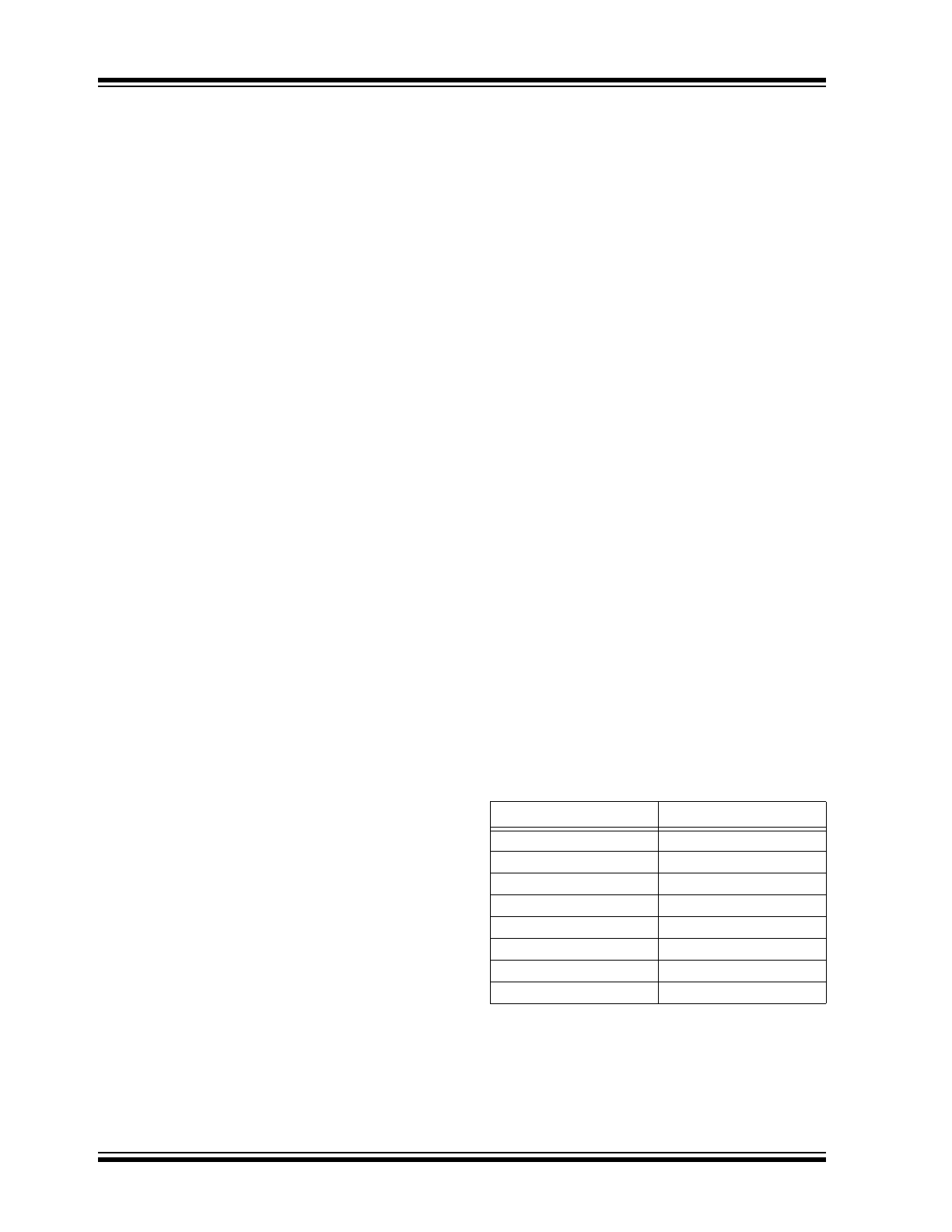
FIGURE 1-1:
PS700 INTERNAL BLOCK DIAGRAM
512
EEPROM
512
EEPROM
32-bit
Accumulators /
Timers
32-bit
Accumulators/
Timers
Voltage
Reference and
Temp Sensor
Voltage
Reference and
Temp Sensor
Voltage
Regulator
Voltage
Regulator
Comm
Interface
Comm
Interface
Registers
Registers
16-Bit
Sigma-Delta
Integrating
A/D Converter
16-Bit
Sigma-Delta
Integrating
A/D Converter
Analog
Input Mux
Analog
Input Mux
Run
Oscillator
Run
Oscillator
VC1
R
OSC
GND
Digital Section
Analog Section
Control and Status
Control and Status
SCL
SR
SDA
Sleep
Oscillator
Sleep
Oscillator
VC2/IO1
NTC/IO0
2004 Microchip Technology Inc.
DS21760F-page 3
PS700
FIGURE 1-2:
APPLICATION SCHEMATIC – PS700-BASED BATTERY PACK
TABLE 1-1:
PIN DESCRIPTIONS
R15
1.0K
R3
221K
R4
680
R5
680
V
CELL
1
2
V
CELL
2
1
NTC
6
SR
8
GND
7
SMB-CLK
3
SMB-DTA
4
R
OSC
5
U1
PS700
R11
470
VR
V1
NTC1
NTC2
PACK CONNECTION
CELL POSITIVE (+)
CELL NEGATIVE (-)
THERMISTOR CONNECTIONS
B+
C
D
B-
R8
0.020
C11
100 nF
C1
100 nF
R7
6.49K
3
1
2
D1
CMSZDA5V6
CONNECTION
GROUND PLANE
C3
1.0 nF
3
4
2
1
5
6
8
7
Q1
SI6880EDQ
V
DD
2
V
SS
3
VM
1
CO
5
DO
4
U2
S8241A
Pin No.
Pin Name
Description
1
VC2/IO1
Cell input connection for lowest cell in a 2-cell series Li Ion pack. Can also be
configured as an open-drain general purpose input/output.
2
VC1
Cell input connection for highest cell in a 2-cell series Li Ion pack. Connects to the
positive terminal of 1-cell series packs. VC1 serves as the power supply input for the
PS700.
3
SCL
SMBus/I
2
C clock line connection.
4
SDA
SMBus/I
2
C data line connection.
5
R
OSC
External bias resistor.
6
NTC/IO0
Input for an external temperature sensor using a 103ETB-type thermistor. Can also
be configured as a general purpose input/output pin.
7
GND
Analog and digital ground.
8
SR
Current measurement A/D input from positive side of the current sense resistor.

PS700
DS21760F-page 4
2004 Microchip Technology Inc.
2.0
ARCHITECTURAL OVERVIEW
The PS700 contains a complete analog “front-end” for
battery monitoring as well as digital logic for control, mea-
surement accumulation, timing and communications.
Major functions within the PS700 include:
• Voltage Regulator
• Precision Time Base
• Temperature Sensor
• 512-Byte EEPROM Memory
• 32-Byte RAM Memory
• Analog-to-Digital (A/D) Converter
• 32-bit Accumulators/Timers
• SMBus/I
2
C Communications Interface
Figure 1-1 is a block diagram of the internal circuitry of
the PS700. Figure 1-2 is a schematic diagram that
depicts the PS700 in a typical single cell Lithium Ion
application. The function of each of the blocks listed
above is summarized in the following sections.
2.1
Internal Voltage Regulator
The PS700 incorporates an internal voltage regulator
that supports 1 or 2-cell series lithium pack configura-
tions. The internal regulator draws power directly from
the VC1 input. No other external components are
required to regulate internal supply voltage.
2.2
Precision Time Base
The integrated precision time base is a highly accurate
RC oscillator that provides precise timing for the sigma-
delta A/D and for the on-chip elapsed time counters
without the need for an external crystal. This time base
is trimmed during manufacturing to a nominal
frequency of 131,072 Hz.
2.3
Temperature Sensor
An integrated temperature sensor is provided that can
eliminate the need for an external thermistor. As an
option, a connection is provided for an external
thermistor for applications where the battery pack is
physically located at a distance away from the PS700.
2.4
EEPROM Memory
512 bytes of EEPROM memory are incorporated for
storage of nonvolatile parameters, such as
PowerSmart
®
3D cell models for use with host driver
firmware. An initialization block is reserved within the
EEPROM array for values that are loaded into PS700
registers following a power-on condition.
2.5
RAM Memory
32 bytes of general purpose RAM memory are
provided for storage of temporary parameters.
2.6
A/D Converter
The PS700 incorporates an integrating sigma-delta
A/D converter together with an analog mux that has
inputs for charge and discharge current, cell and pack
voltages, the on-chip temperature sensor and an off-
chip thermistor. The converter can be programmed to
perform a conversion with resolutions of 8 to 15 bits plus
sign while utilizing either a ±340 mV or a ±170 mV
reference.
2.7
32-Bit Accumulators/Timers
The PS700 incorporates four 32-bit accumulators and
four 32-bit elapsed time counters. The Discharge
Current Accumulator (DCA) and the Charge Current
Accumulator (CCA) are intended to record discharge
and charge capacity values. The Discharge Time
Counter (DTC) and the Charge Time Counter (CTC)
are intended to maintain the total discharge time and
charge time. Accumulated charge and discharge
values can be used to determine state of charge of the
battery as well as cycle count information. With
information provided by the elapsed time counters,
average charge and discharge currents over an
extended period of time can be calculated.
2.8
SMBus/I
2
C Communications
Interface
The communications port for the PS700 is a 2-wire
industry standard SMBus/I
2
C interface. All commands,
status and data are read or written from the host
system via this interface.
2004 Microchip Technology Inc.
DS21760F-page 5
PS700
3.0
OPERATIONAL DESCRIPTION
3.1
A/D and Accumulator/Timer
Operation
3.1.1
A/D CONVERSION CYCLE
When the A/D converter is enabled and active, it
repeatedly performs a cycle of 1 to 8 conversions as
programmed by the user through 8 A/D Control
registers. These registers determine the input source,
resolution, reference voltage source and sequence of
conversions during an A/D converter cycle. During the
cycle, the A/D logic accesses each register in
sequence and performs the conversion specified by the
bits within the register. This register contains an enable
bit, a resolution field, a select bit for a single-ended or
differential reference and a select field for the analog
input mux. The results from each conversion are stored
in one of eight corresponding16-bit result registers.
If the “enable” bit is set within a control register, a
conversion will be performed. If it is disabled, that
conversion will be skipped and the logic will move on to
the next register. In this manner, the user can specify a
sequence of conversions that will be performed during
each A/D cycle.
As stated above, the input source for each of the
registers is programmable. The 3-bit mux field within
each control register selects one of seven possible
input sources for the A/D conversion. The list of input
sources is as follows:
• Charge/Discharge Current (voltage from SR pin to
GND)
• Internal Temperature Sensor
• External Thermistor (constant current source on
NTC pin)
• Battery Pack Voltage
• VC1 Voltage
• VC2 Voltage
• A/D Offset (conversion performed with input
shorted internally to determine offset error
associated with the converter)
However, the accumulator/timer functions are “hard
wired” to specific A/D Result registers. For this reason,
the control/result registers are given names which
indicate their primary intended usage (see Table 3-1).
TABLE 3-1:
A/D CONTROL/RESULT REGISTERS
The 3-bit “resolution” field in each A/D Control register
determines the resolution of the conversion, from a
minimum of 9 bits (8 bits plus sign bit) to a maximum of
16 bits (15 bits plus sign bit). The time required to
complete the conversion is a function of the number of
bits of resolution (n) selected. The conversion time can
be calculated as follows:
T
ADC
= 30.52
µs * 2
n
where:
“n” is the number of bits of resolution selected
The “Ref” bit selects the magnitude of the reference
voltage. Either a ±340 mV or a ±170 mV reference is
available. The ±170 mV reference is typically used for
current readings and the ±340 mV reference for all
other measurements.
The value of the LSB can be expressed as a function of
the resolution selected as follows:
A/D LSB = 680/340 mV/2
n
where:
“n” is the number of bits of resolution selected
The result value is given in sign/magnitude format (i.e.,
a sign bit with a 15-bit magnitude).
A/D Register #
Control Register
Result Register
Intended Input Source
0
Ictrl
Ires
Battery Pack Current (via sense resistor)
1
ITctrl
ITres
Internal Temperature Sensor
2
ETctrl
ETres
External Temperature Sensor
3
VPctrl
VPres
Battery Pack Voltage (VC1 to GND)
4
VC1ctrl
VC1res
Battery Cell Voltage (VC1 to VC2)
5
VC2ctrl
VC2res
Battery Cell Voltage (VC2 to GND)
6
OFFSctrl
OFFSres
Internal A/D Offset Voltage (A/D input automatically
internally shorted to GND)
7
AUXctrl
AUXres
Any
15
0
S
Magnitude
PS700
DS21760F-page 6
2004 Microchip Technology Inc.
3.1.2
CURRENT MEASUREMENT
Charge and discharge currents are measured using a
5 to 600 m
Ω
sense resistor that is connected between
the SR and GND pins. The maximum input voltage at
SR is ±150 mV. The sense resistor should be properly
sized to accommodate the systems lowest and highest
expected charge and discharge currents including
suspend and/or standby currents.
In order to perform charge and discharge current
measurements, the Ictrl register must be programmed
with the SR pin as the analog input source. If charge
and discharge accumulation is desired, the Ictrl and
corresponding Ires registers should be used to select
current measurement since the DCA, DTC, CCA and
DCA registers are updated by the measurement results
from the Ires register.
Ictrl programming in a typical application is as follows.
TABLE 3-2:
Ictrl PROGRAMMING
Using the maximum resolution of 16 bits, the voltage
value of the LSB is:
A/D LSB = 340 mV/2
16
= 5.19
µV
Using a sense resistor value of 20 m
Ω
, the value of the
LSB in units of current is:
5.19
µV/20 mΩ = 259 µA
3.1.3
VOLTAGE MEASUREMENTS
Analog mux inputs are provided to support measure-
ment of individual cell and battery pack voltages. A/D
control registers VPctrl, VC1ctrl and VC2ctrl are used
to specify the measurement to be made. In typical
applications, voltage measurement at the cell or pack
level is done using the +340 mV reference and a
resolution of 10 bits plus sign bit.
The value of the LSB in a pack voltage measurement
using a 340 mV reference voltage is given by the formula:
V
PACK
LSB = 10.2V/2
n
Where “n” is the resolution selected. For typical
applications where n = 10:
V
PACK
LSB = 10.2V/2
10
= 10.2V/1024 = 9.96 mV
The value of the LSB in a cell voltage measurement
using a 340 mV reference voltage is given by the
formula:
V
CELL
LSB = 6.23V/2
n
Where “n” is the resolution selected. For typical
applications where n = 10:
V
CELL
LSB = 6.23V/2
10
= 6.23V/1024 = 6.08 mV
The following table shows LSB values for 9-bit plus
sign resolution, so n = 9.
TABLE 3-3:
LSB VALUES FOR 10-BIT
RESOLUTION
VPctrl programming in a typical application is as
follows.
TABLE 3-4:
VPctrl PROGRAMMING
The input source fields for the VPctrl, VC1ctrl and
VC2ctrl registers must be programmed to select pack
voltage (on VC1), VC1 cell voltage and VC2 cell
voltage in order for these registers to control their
intended measurements.
3.1.4
TEMPERATURE MEASUREMENTS
A/D input channels are provided for temperature mea-
surement using either the internal temperature sensor
or an external thermistor.
3.1.4.1
Internal Temperature
The output of the internal temperature sensor is a volt-
age range with limits that correspond to operating
temperature limits as follows:
-20°C
→
239 mV
+70°C
→
312 mV
The output voltage of the internal sensor as a function
of temperature can be given as:
V
IT
(mV) = 239 + 0.82 * (T + 20)
Defined within the ITctrl registers are the settings for
the reference utilized and the resolution desired for
measurement of temperature using the internal tem-
perature sensor. Because of input voltage range
described above, the 340 mV reference should be
selected. Typically, 10-bit plus sign of resolution are
selected which results in the following temperature
resolution:
LSB (Voltage) = Full Scale Range/# of steps
= 340 mV/2
10
= 332
µV/LSB
LSB (°C)
= 332
µV/LSB * (1 / 820) °C/µV
= 0.404°C/LSB
Bit(s)
Name
Value
Function
7
En
1
Enables A/D conversion
6-4
Res
111
Selects 16-bit resolution
3
Ref
0
Selects ±170 mV reference
2-0
Sel
000
Selects V
SR
as converter input
Measurement
VR
Divider
Bits
LSB
V
PACK
340
1/30
9 + sign
19.92
V
CELL
340
1/18.33
9 + sign
12.17
Bit(s)
Name
Value
Function
7
En
1
Enables A/D conversion
6-4
Res
001
Selects 10-bit resolution
3
Ref
1
Selects ±340 mV reference
2-0
Sel
011
Selects V
SR
as converter input

2004 Microchip Technology Inc.
DS21760F-page 7
PS700
3.1.4.2
External Temperature
For temperature measurement using an external sensor,
the NTC pin supplies a constant current source of
12.5
µ
A. For proper operation, an industry standard
10 kOhm at 25°C negative temperature coefficient
(NTC) device of the 103ETBtype, should be connected
between NTC and GND. The NTC reference output is
only enabled during an external temperature
measurement in order to minimize power consumption.
The output of the current source, connected to the
external thermistor, produces a voltage range with
limits that correspond to operating temperature limits,
as follows:
-20°C
→
263 mV
+70°C
→
317 mV
The output voltage of the external sensor as a function
of temperature can be given as:
V
EX
(mV) = 263 + 0.6 * (T + 20)
Defined within the ETctrl registers are the settings for the
reference utilized and the resolution desired for mea-
surement of temperature using the external temperature
sensor. Again, the 340 mV reference should be
selected. The following temperature results in a 10-bit
conversion:
LSB (Voltage) = Full Scale Range/# of steps
= 340 mV/2
10
= 332
µV/LSB
LSB (°C)
= 332
µV/LSB * (1/600)°C/µV
= 0.553°C/LSB
3.1.5
OFFSET COMPENSATION
The host software can perform offset compensation by
using an offset measurement value read from the
PS700. When the offset calibration is enabled within
the OFFSctrl register, the converter inputs are
internally shorted together and an A/D conversion is
performed at the specified resolution. The offset value
is stored in the OFFSres register.
3.1.6
ACCUMULATION/TIMING
The PS700 incorporates four 32-bit accumulators and
four 32-bit elapsed time counters. The Discharge Current
Accumulator (DCA) and the Charge Current Accumula-
tor (CCA) are intended to record discharge and charge
capacity values. The Discharge Time Counter (DTC) and
the Charge Time Counter (CTC) are intended to maintain
the total discharge time and charge time. Accumulated
charge and discharge values can be used to determine
state of charge of the battery as well as cycle count infor-
mation. With information provided by the elapsed time
counters, average charge and discharge currents over
an extended period of time can be calculated.
Each of the four 32-bit accumulator registers is assigned
a fixed “source” A/D Result register. When the accumu-
lator is enabled, it is updated every 500 ms by adding the
contents of the assigned result register value to the
previous accumulator value. The accumulators are
listed in Table 3-5 with their assigned source registers.
TABLE 3-5:
ACCUMULATOR REGISTERS
The resolution of the accumulated value is equal to the
resolution selected for the associated conversion, up to
a converter resolution of 15-bit plus sign. If a 15-bit plus
sign A/D value is being accumulated, then the
accumulator resolution in microvolt seconds is:
Accumulator LSB (
µVs) = (Full Scale Range/# of steps)
* 0.5s = (340 mV/2
15
) * 0.5s
= 5.19
µVs
3.1.7
CHARGE/DISCHARGE
ACCUMULATORS
The DCA register is intended to accumulate discharge
current and the CCA register is intended to accumulate
charge current. Both use the Ires register as its source.
For this reason, in most applications, current measure-
ment defined in the A/D Control registers should be
programmed to measure current by reading the voltage
across the Sense Resistor pin (SR).
During charging, a negative voltage will exist across
the SR pin to ground. Following a conversion, a
positive voltage measurement results in the sign bit =
0
in the Ires register. When the sign bit =
0
, the measured
result will be added to the CCA register contents and
the sum is returned to CCA.
In this way, the total charge current will be accumulated
in CCA.
Similarly, during discharge, a positive voltage will exist
between the SR pin and ground. In this case, the
conversion will result with sign bit =
1
in the Ires regis-
ter, indicating a negative value or discharge current
condition. Under this condition, the DCA register will be
updated with the discharge current measured during
that conversion.
The value stored in the DCA or CCA register can be
interpreted as illustrated in the following example.
Using a 16-bit signed conversion for current measure-
ment and a 20 m
Ω
sense resistor, the LSB can be
expressed in units of capacity in micro amp seconds as
follows:
Accumulator LSB (
µAs) = Voltage LSB/R
SENSE
=
(2.59
µVs)/20 mΩ = 130 µAs
The “Accum” bit in the Accumctrl register must be
enabled for accumulation to occur in both the CCA and
DCA registers.
Abbr.
Accumulator Name
Source
DCA
Discharge Current
Accumulator
Ires (Sign bit =
1
)
CCA
Charge Current
Accumulator
Ires (Sign bit =
0
)
TA
Temperature Accumulator
ITres or ETres
VC2A
VC2 Accumulator
VC2res
PS700
DS21760F-page 8
2004 Microchip Technology Inc.
3.1.8
CHARGE/DISCHARGE TIME
COUNTERS
The Charge Time Counter (CTC) will increment at the
rate of 2 counts every second as long as a negative
voltage is measured at the SR pin. The CTC can
thereby maintain a time count representing the total
time that charge current has flowed into the battery.
The Discharge Time Counter (DTC) will increment at
the rate of 2 counts every second as long as a positive
voltage is measured at the SR pin. The DTC can
thereby maintain a time count representing the total
time that discharge current has flowed from the battery.
3.1.9
GENERAL PURPOSE
ACCUMULATORS
There are two general purpose accumulators, TA and
VC2A. For typical applications, these accumulators
have been assigned specific functions. The user can
redefine the use of these accumulators to fit the design
requirements.
TA can be used to accumulate results from the ITres or
ETres registers. Accumulation to TA must be enabled
in the Accumctrl register bit “AccT”. The selection for
accumulation of the values represented by the internal
or external thermistor is also determined in the
Accumctrl register bit “tsel”.
VC2A can be used to accumulate results from VC2res.
Accumulation in VC2A must be enabled in the
Accumctrl register bit “AccV”. The value stored in
VC2res corresponds to the measurement as defined in
the A/D Control register VC2ctrl. This function is
utilized if the VC2 pin is configured as an independent
A/D input and not connected to the cell stack.
The “Accum” bit in the Accumctrl register must be
enabled for accumulation to occur in TA and VC2A.
3.1.10
GENERAL PURPOSE TIMERS
There are two general purpose timers that are enabled
by accumulation in the TA and VC2A accumulators.
TAT is used to maintain a time count during accumula-
tion in the TA register. This timer increments at a
frequency of 2 counts every second.
VC2T is used to maintain a time count during
accumulation in the VC2A register. This timer
increments at a frequency of 2 counts every second.
3.2
Power Modes
The PS700 has four operational power modes: Run,
Sample, Sample-Sleep and Shelf-Sleep. Each con-
sumes power according to the configuration settings as
described in the following sections.
3.2.1
RUN MODE
During Run mode, the PS700 performs continuous A/D
conversion cycles per the programming of the A/D
conversion cycle documented in Section 3.1.1 “A/D
Conversion Cycle”. As described above, during each
cycle, between 1 and 8 conversions are performed and
the accumulators/time counters are updated as
programmed by the user.
Run mode is entered following a Power-on Reset when
the pack voltage (V
PACK
) applied on the VC1 pin rises
above the V
POR
threshold. Run mode can also
be entered from the Sample, Sample-Sleep and
Shelf-Sleep modes as described below.
The PS700 will remain in Run mode as long as the pack
voltage is above the V
POR
threshold and the Sample,
Sample-Sleep and Shelf-Sleep modes are not active.
3.2.2
SAMPLE MODE
In Sample mode, A/D measurements are not continu-
ously performed as in Run mode. Instead, they are
performed at a user selectable rate. The purpose of
Sample mode is to reduce power consumption during
periods of low rate charge or discharge. The power
advantage of Sample mode comes from the reduction
in frequency of A/D measurements.
Sample mode is entered by programming the “Samp”
bit =
1
in the A/D Configuration register. The PS700 will
remain in Sample mode as long as “Samp” bit =
1
and
the VC1 voltage is above the V
POR
threshold and the
Sample-Sleep and Shelf-Sleep modes are not active.
Run mode will be resumed when the Samp bit is
cleared to ‘
0
’.
The Sample mode rate is selected using the “SampDiv”
bits within the A/D Configuration register. The sample
interval is 2**(SampDiv) * 0.5 sec. The possible sample
rate intervals are as follows.
TABLE 3-6:
SAMPLE RATE INTERVALS
In Sample mode, much of the analog circuitry remains
on. Therefore, the power savings are not as great as in
Sample-Sleep mode (described below). Refer to
Section 6.0 “Electrical Characteristics” for a specifi-
cation of the amount of current consumed in Sample
mode.
“SampDiv”
Sample Interval
Value = 0
0.5s
Value = 1
1.0s
Value = 2
2.0s
Value = 3
4.0s
Value = 4
8.0s
Value = 5
16.0s
Value = 6
32.0s
Value = 7
64.0s

2004 Microchip Technology Inc.
DS21760F-page 9
PS700
3.2.3
SAMPLE-SLEEP MODE
In Sample-Sleep mode, the PS700 goes into the Sleep
state and wakes up at user-programmed intervals to
perform a set of conversions as programmed for the
A/D cycle. The purpose of Sample-Sleep is to achieve
the minimum power consumption possible while
periodically measuring specified parameters.
While the PS700 is in the Sleep portion of Sample-
Sleep interval, all of the analog circuitry is shut off. The
Sleep interval time is driven by an independent low-
power on-chip RC oscillator that is separate from the
primary oscillator. The Sleep oscillator consumes much
less power than the primary oscillator, but is less
accurate. While in Sample-Sleep mode, the device
consumes average current in the range of 20
µ
A.
During the active portion of Sample-Sleep mode, a
single set of conversions is performed and a Run mode
current in the range of 85
µ
A will be consumed for the
duration of the measurements.
Sample-Sleep mode is invoked by one of the following
actions:
1.
Cell voltage on VC1 or VC2 drops below the trip
point programmed in the VCtrip register with the
corresponding “VC1ent” or “VC2ent” bit set in
the TRIPctrl register. This action can be used to
prevent excessive battery discharge in the event
of a dangerously low cell voltage. Be aware that
Sample-Sleep will not be entered if the “lex” bit
is set, enabling wake-up based on charge
current and the measured current is above the
threshold set in the I+trip register.
2.
Setting the SSLP bit in the OpMode register.
The host can take this action when the system is
entering a low-power standby condition and it is
desired to periodically measure and accumulate
current, voltage, or temperature.
3.
Current less than the I-trip register value when
“Ient” bit is set in the TRIPctrl register.
The Sample-Sleep interval is determined by the
programming of the “Sampdiv” bits within the A/D Con-
figuration register, together with the “SSLPdiv” bits
within the OpMode register. The sample interval is
2**(Sampdiv) * 2**(SSLPdiv) * 0.5 sec. The possible
Sample-Sleep interval time, therefore, ranges from a
minimum of 0.5 sec to over 136 minutes.
Exit from Sample-Sleep mode to Run mode can be
accomplished by clearing the “SSLP” bit or by program-
ming a wake-up based on pack voltage or current.
Wake-up based on charge current will occur when the
“Iex” bit is set in the TRIPctrl register and the charging
current value is above the threshold programmed in the
I+trip register. Wake-up based on pack voltage will
occur when the “VPex” bit is set in the TRIPctrl register
and the pack voltage rises above the threshold
programmed in the SStrip register.
3.2.4
SHELF-SLEEP MODE
Shelf-Sleep mode is the lowest power mode and is
intended to preserve battery capacity when the battery
pack is shipped or stored or if the battery voltage drops
below a specified threshold. While in Shelf-Sleep
mode, no measurements occur, no accumulation is
performed and no SMBus communications are
recognized. In addition, volatile memory is not
maintained.
Entry to Shelf-Sleep mode is enabled by programming
the “SHent” bit =
1
or if V
PACK
is less than VPtrip. The
Shelf-Sleep mode will then be entered when the
SMBus pins (both SDA and SCL) drop from a high to a
low level for a minimum time period specified by t
SHELF
.
This action will also occur if the battery pack is
physically disconnected from the system.
Exit from the Shelf-Sleep mode back to Run mode will
occur when the SMBus pins (both SDA and SCL) are
both pulled from a low to high condition and remain
high for a minimum time of t
WAKE
, signifying system
activity or the connection of the pack to the host.
3.3
General Purpose Input/Outputs
The NTC and VC2 pins have alternate functions of
general purpose I/O; IO0 and IO1, respectively. These
pins can be configured as digital general purpose
inputs/outputs if their normal application functions of
temperature and cell monitoring are not needed. Their
configuration is controlled in the GPIOctrl register.
The IO0 (NTC) pin may be configured as a push-pull
output, an open-drain driver with internal pull-up, or as
a tri-stated pin. When configured as a push-pull or
open-drain output, the output high voltage is the 3.0V
internally regulated supply. When the output function is
disabled, an external circuit may drive the pin as an
input with a voltage range of 0-3.0V. The input function
may be used whether or not the pin is driven by the
PS700. In addition, the input function may be disabled,
in which case the input buffer is powered down,
preventing current drain if the NTC pin rests at an
intermediate level.
The IO1 (VC2) pin is similar to that of NTC except it is
an open-drain output only. IO1 has no explicit output
enable control; therefore, if the output is set to a logic
‘
1
’, the internal pull-down is turned off which tri-states
the pin. The input function is the same as IO0.
Note:
If the IO0 and/or IO1 pins are being used
for their analog functions, their respective
GPIO output and input functions must be
disabled. The GPIO function may be
totally disabled by clearing the appropriate
GPIOctrl bit.

PS700
DS21760F-page 10
2004 Microchip Technology Inc.
3.4
SMBus/I
2
C Interface
The PS700 supports a 2-wire bidirectional bus and
data transmission protocol that is fully compatible with
the industry standard SMBus V1.1 based on the I
2
C
interface. This interface is used to read and write data
from/to the on-chip registers and EEPROM. The device
responds to the same SMBus slave address for access
to all functions. The following is a brief overview of the
SMBus/I
2
C operational implementation in the PS700.
Please refer to the SMBus v1.1 specification for
complete operational details of this industry standard
interface. This specification can be obtained at the
SMBus Implementer’s Forum web site at
www.smbus.org.
3.4.1
SMBus OVERVIEW
SMBus is a two-wire multi-master bus, meaning that
more than one device capable of controlling the bus
can be connected to it. A master device initiates a bus
transfer and provides the clock signals. A slave device
can receive data provided by the master or can in
return provide data to the master.
Since more than one device may attempt to take
control of the bus as a master, SMBus provides an
arbitration mechanism based on I
2
C and relying on the
wired-AND connection of all SMBus devices residing
on the bus. If two or more masters try to place informa-
tion on the bus, the first to produce a “one” when the
other(s) produce a “zero” loses arbitration and has to
release the bus.
The clock signals during arbitration are a wired-AND
combination of all the clocks provided by SMBus
masters. Bus clock signals from a master can only be
altered by clock stretching or by other masters and only
during a bus arbitration situation. In addition to bus
arbitration, SMBus implements the I
2
C method of clock
low extending in order to accommodate devices of
different speeds on the same bus.
SMBus version 1.1 can be implemented at any voltage
between 3 and 5 Volts ±10%. Devices can be powered
by the bus V
DD
or by their own power source (such as
Smart Batteries) and they will interoperate flawlessly as
long as they adhere to the SMBus electrical
specifications.
3.4.2
SMBus DATA TRANSFERS
A device that sends data onto the SMBus is defined as
a transmitter and a device receiving data as a receiver.
The device that controls the message is called a
“master”. The devices that are controlled by the master
are “slaves”. The SMBus must be controlled by a
master device that generates the serial clock (SCL),
controls the bus access and generates Start and Stop
conditions. The PS700 operates as a slave on the two-
wire bus. Connections to the bus are made via the
open-drain I/O lines SDA and SCL.
SMBus operates according to the following bus
protocol:
• Data transfer may be initiated only when the bus
is not busy.
• During data transfer, the data line must remain
stable whenever the clock line is high. Changes in
the data line while the clock line is high will be
interpreted as control signals.
The SMBus specification defines the following bus
conditions:
Bus Not Busy: Both data and clock lines remain high.
Start Data Transfer: A change in the state of the data
line from high to low, while the clock is high, defines a
Start condition.
Stop Data Transfer: A change in the state of the data
line from low to high, while the clock line is high, defines
the Stop condition.
Data Valid: The state of the data line represents valid
data when, after a Start condition, the data line is stable
for the duration of the high period of the clock signal.
The data on the line must be changed during the low
period of the clock signal. There is one clock pulse per
bit of data. Each data transfer is initiated with a Start
condition and terminated with a Stop condition. The
number of data bytes transferred between Start and
Stop conditions is not limited and is determined by the
master device. The information is transferred byte-wise
and each receiver Acknowledges with a ninth bit.
Acknowledge:
Each receiving device, when
addressed, is obliged to generate an Acknowledge bit
after the reception of each byte. The master device
must generate an extra clock pulse which is associated
with this Acknowledge bit.
A device that Acknowledges must pull down the SDA
line during the Acknowledge clock pulse in such a way
that the SDA line is stable low during the high period of
the Acknowledge related clock pulse. Of course, setup
and hold times must be taken into account. A master
must signal an end of data to the slave by not generat-
ing an Acknowledge bit on the last byte that has been
clocked out of the slave. In this case, the slave must
leave the data line high to enable the master to
generate the Stop condition.