

2004 Microchip Technology Inc.
DS21902A-page 1
PS501-0901
• Single chip solution for rechargeable battery
management
• Footprint compatible with PS402
• SMBus 1.1 and SBData 1.1 compatible
• Precise capacity reporting for NiMH and NiCd
battery chemistries
• Embedded Microchip patented Accuron
®
technology contained in customizable on-chip
16-Kbyte Flash memory
• User configurable and “learned” parameters
stored in on-chip 256 x 8 EEPROM
• Algorithms and parameters fully field
reprogrammable via SMBus interface
• Integrating sigma-delta A/D converter with 9 to
16-bit programmable resolution which accurately
measures:
- Current through sense resistor
- High-voltage (18V) battery cells directly
connected to V
CELL
inputs
- Temperature measurement from on-chip
sensor or optional external thermistor
• Integrated precision silicon time base
• Twelve individually programmable input/output
pins that can be assigned as charge control I/O,
secondary safety function I/O, SOC LED output or
general purpose I/O
- Two of the twelve I/Os are high-voltage,
capable for direct drive of charge and safety
FETs
• On-chip regulator generates precision digital and
analog supply voltages directly from pack voltage
• Flexible power operating modes:
- Run: Continuous operation
- Sample: Periodic measurements at
programmable intervals
- Sleep: Shutdown mode due to low voltage;
power consumption less than 25
µ
A
- Shelf-Sleep: Shuts off PS501-0901 power
consumption for pack storage with automatic
wake-up on pack insertion; power
consumption is less than 1
µ
A
• Integrated Reset Control
- Power-on Reset
- Watchdog Timer Reset
- Brown-out Detection Reset
Pin Description
Pin Summary
Pin Name
Type
Description
V
DDD
, V
SSD
Supply Digital supply voltage input,
ground
GPIO(0..9)
I/O
Programmable digital I/O
GPIOHV1,2
I/O
Open-drain programmable
digital I/O for direct drive of
FETs
MCLR
I
Master Clear; pull-up in
normal operation
SMB-CLK,
SMB-DTA
I/O
SMBus interface
VC(1)
I
Pack voltage input
V
DDA
, V
SSA
Supply Voltage regulator output
(internally connected to
analog supply input); ground
RSHP, RSHN
I
Current sense resistor input
V
NTC
I
External thermistor input
V
REFT
O
Thermistor reference voltage
R
OSC
I
Internal oscillator bias resistor
RSV1 -3
I
Reserved pins
2
3
4
5
6
7
8
9
28
27
26
25
24
23
22
21
20
PS
501-0901
28-Pin SSOP Package (0.209 mil)
1
10
19
V
DDD
GPIO(4)
GPIO(5)
GPIO(6)
GPIO(7)
SMB-CLK
SMB-DTA
RSV1
RSV2
RSV3
V
SSD
GPIO(3)
GPIO(2)
GPIO(1)
GPIO(0)
GPIOHV2
MCLR
GPIOHV1
GPIO(9)
GPIO(8)
11
12
13
14
VC(1)
V
DDA
V
SSA
RSHP
18
17
16
15
R
OSC
V
REFT
V
NTC
RSHN
Single Chip Field Reprogrammable Battery Manager –
Nickel Chemistries
PS501-0901
DS21902A-page 2
2004 Microchip Technology Inc.
1.0
PRODUCT OVERVIEW
The PS501-0901 combines a high-performance, low-
power Microchip PIC18 microcontroller core, together
with PowerSmart
®
proprietary monitor/control
algorithms and 3D cell models, stored in 16 Kbytes of
on-chip reprogrammable Flash memory.
Analog resources include a 16-bit sigma-delta integrat-
ing A/D and mixed signal circuitry for precision
measurement of battery current, temperature and
voltage. On-chip EEPROM is provided for storage of
user customizable and “learned” battery parameters.
An industry standard 2-wire SMBus interface supports
host communication using standard SBData
commands and status.
Additional integrated features include a high accuracy
on-chip oscillator and temperature sensor. Twelve
general purpose pins support charge or safety control
or user programmable digital I/O. Eight of them can be
used as LED drivers and two are open drain for direct
FET drive.
The PS501-0901 can be configured to accommodate
all Nickel rechargeable battery chemistries, including
NiMH and NiCd. Nickel battery packs must contain
between six and twelve series cells.
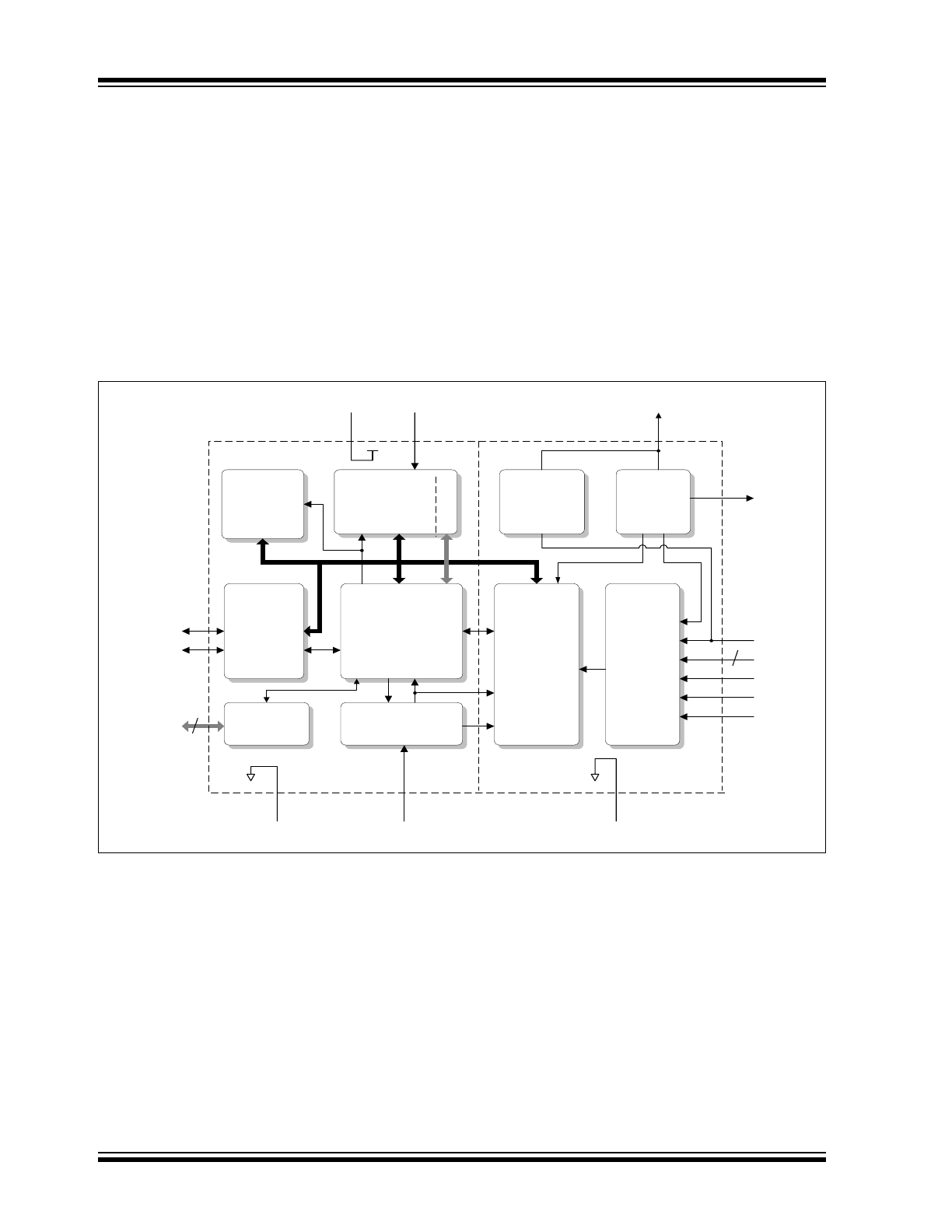
FIGURE 1-1:
PS501-0901 INTERNAL BLOCK DIAGRAM
256-byte
EEPROM
256-byte
EEPROM
16-Kbyte
FLASH
16-Kbyte
FLASH
De
c
o
d
e
r
Regulator
Regulator
Voltage
Reference
and
Tem perature
Sensor
Voltage
Reference
and
Tem perature
Sensor
SM Bus
Interface
SMBus
Interface
PIC18
Microcontroller
Core
PIC18
Microcontroller
Core
16-Bit
Sigm a-Delta
Integrating
A/D Converter
16-Bit
Sigm a-Delta
Integrating
A/D Converter
Analog
Input Mux
Analog
Input Mux
Program m able
Digital
Input/Output
Program m able
Digital
Input/Output
Silicon Oscillator
Silicon Oscillator
R
O SC
SMB-CLK
RSHN
V
NTC
V
DDA
12
V
REFT
3
V
DDD
V
PP
SM B-DTA
V
SS D
GPIO(11-0)
D igital Section
Analog Section
V
S SA
RSHP
RSV1-3
VC(1)

2004 Microchip Technology Inc.
DS21902A-page 3
PS501-0901
1.1
Architectural Description
The PS501-0901 is a a fully field reprogrammable single
chip solution for rechargeable battery management.
Figure 1-1 is an internal block diagram highlighting the
major architectural elements described below.
1.2
Microcontroller/Memory
The PS501-0901 incorporates an advanced, low-
power Microchip PIC18 8-bit RISC microcontroller
core. Memory resources include 16 Kbytes of repro-
grammable Flash memory for program/data storage
and 256 bytes of EEPROM for parameter storage. Both
memory arrays may be reprogrammed through the
SMBus interface.
1.3
A/D Converter
The PS501-0901 performs precise measurements of
current, voltage and temperature, using a highly
accurate 16-bit integrating sigma-delta A/D converter.
The A/D can be calibrated to eliminate gain and offset
errors and incorporates an auto-zero offset correction
feature that can be performed while in the end system
application.
1.4
Microchip Firmware/Battery Models
Contained within the 16-Kbyte Flash memory is the
Microchip developed battery management firmware
that incorporates proprietary algorithms and sophisti-
cated 3-dimensional cell models. Developed by battery
chemists, the patented, self-learning 3D cell models
contain over 250 parameters and compensate for self-
discharge, temperature and other factors. In addition,
multiple capacity correction and error reducing
functions are performed during charge/discharge
cycles to enhance accuracy and improve fuel gauge
and charge control performance. As a result, accurate
battery capacity reporting and run-time predictions with
less than 1% error are achievable.
The reprogrammability of the Flash allows firmware
upgrades and customized versions to be rapidly
created without the need for silicon revisions.
The PS501-0901 can be easily customized for a
particular application’s battery cell chemistry. Standard
configuration files are provided by Microchip for a wide
variety of popular rechargeable cells and battery pack
configurations.
1.5
SMBus Interface/SBData
Commands
Communication with the host is fully compliant with the
industry standard Smart Battery System (SBS)
specification. Included is an advanced SMBus
communications engine that is compliant with the
SMBus v1.1 protocols. The integrated firmware
processes all the revised Smart Battery Data (SBData)
v1.1 values.
1.6
Accurate Integrated Time Base
The PS501-0901 provides a highly accurate RC
oscillator that provides accurate timing for self-
discharge and capacity calculations and eliminates the
need for an external crystal.
1.7
Temperature Sensing
An integrated temperature sensor is provided to
minimize component count when the PS501-0901 IC is
located in close physical proximity to the battery cells
being monitored. As an option, a connection is
provided for an external thermistor that can also be
monitored.
1.8
General Purpose I/O
Twelve programmable digital input/output pins are
provided by the PS501-0901. Eight of these pins can
be used as LED outputs to display State-Of-Charge
(SOC) or for direct control of external charge circuitry.
Alternatively, they can be used as general purpose
input/outputs. Two of the I/Os are open-drain outputs
and can thus be used to directly drive FETs or other
high-voltage applications.

PS501-0901
DS21902A-page 4
2004 Microchip Technology Inc.
TABLE 1-1:
PIN DESCRIPTIONS
Pin
Name
Description
1
V
DDD
(Input) Filter capacitor input for digital supply voltage.
2
GPIO(4)
(Bidirectional) Programmable general purpose digital input/output pin (4) or LED driver.
3
GPIO(5)
(Bidirectional) Programmable general purpose digital input/output pin (5) or LED driver.
4
GPIO(6)
(Bidirectional) Programmable general purpose digital input/output pin (6) or LED driver.
5
GPIO(7)
(Bidirectional) Programmable general purpose digital input/output pin (7) or LED driver.
6
SMB-CLK
SMBus clock pin connection.
7
SMB-DTA
SMBus data pin connection.
8
RSV1
Reserved – Must be connected to ground.
9
RSV2
Reserved – Must be connected to ground.
10
RSV3
Reserved – Must be connected to ground.
11
VC(1)
(Input) Pack voltage input.
12
V
DDA
(Input) Analog supply voltage input.
13
V
SSA
Analog ground reference point.
14
RSHP
(Input) Current measurement A/D input from positive side of the current sense resistor.
15
RSHN
(Input) Current measurement A/D input from negative side of the current sense resistor.
16
V
NTC
(Input) A/D input for use with an external temperature circuit. This is the midpoint
connection of a voltage divider where the upper leg is a thermistor (103ETB type) and
the lower leg is a 3.65 kOhm resistor. This input should not go above 150 mV.
17
V
REFT
(Output) Reference voltage output for use with temperature measuring A/D circuit. This
150 mV output is the top leg of the voltage divider and connects to an external
thermistor.
18
R
OSC
External bias resistor.
19
GPIO(8)
(Bidirectional) Programmable general purpose digital input/output pin (8).
20
GPIO(9)
(Bidirectional) Programmable general purpose digital input/output pin (9).
21
GPIOHV1
(Bidirectional) Programmable general purpose digital input/output pin (10).
Open-drain, high-voltage tolerant.
22
MCLR
(Input) Master Clear. Must be pulled up for normal operation.
23
GPIOHV2
(Bidirectional) Programmable general purpose digital input/output pin (11).
Open-drain, high-voltage tolerant.
24
GPIO(0)
(Bidirectional) Programmable general purpose digital input/output pin (0) or LED driver.
25
GPIO(1)
(Bidirectional) Programmable general purpose digital input/output pin (1) or LED driver.
26
GPIO(2)
(Bidirectional) Programmable general purpose digital input/output pin (2) or LED driver.
27
GPIO(3)
(Bidirectional) Programmable general purpose digital input/output pin (3) or LED driver.
28
V
SSD
Digital ground reference point.
2004 Microchip Technology Inc.
DS21902A-page 5
PS501-0901
2.0
A/D OPERATION
The PS501-0901 A/D converter measures voltage,
current and temperature and integrates the current
over time to measure State-Of-Charge. The voltage of
the entire pack is monitored and the pack is calibrated
for accuracy. Using an external sense resistor, current
is monitored during both charge and discharge and is
integrated over time using the on-chip oscillator as the
time base. Temperature is measured from the on-chip
temperature sensor or an optional external thermistor.
Current and temperature are also calibrated for
accuracy.
2.1
A/D Converter List
The A/D converter alternately measures pack voltage,
current, temperature and auto-offset as explained
below. The schedule for the sequence and frequency of
these measurements is programmable, as is the num-
ber of bits used. The default scheduling uses four lists.
At near full (above the voltage point ADLNearFull) and
near empty (below the voltage point ADLNearEmpty),
voltage intensive lists are used to accurately end
charge or discharge. In between ADLNearFull and
ADLNearEmpty, a current intensive schedule is used
to more accurately calculate capacity.
2.2
Current Measurement
The A/D input channels for current measurement are
the RSHP and RSHN pins. The current is measured
using an integrating method, which averages over time
to get the current measurement and integrates over
time to get a precise measurement value.
A 5 to 600 milliohm sense resistor is connected to
RSHP and RSHN in a typical application schematic.
The maximum input voltage at either RSHP or RSHN is
+/-150 mV. The sense resistor should be properly sized
to accommodate the lowest and highest expected
charge and discharge currents, including suspend and/
or standby currents.
Circuit traces from the sense resistor should be as
short as practical without significant crossovers or
feedthroughs. Failure to use a single ground reference
point at the negative side of the sense resistor can
significantly degrade current measurement accuracy.
The EEPROM value, NullCurr, represents the zero
zone current of the battery. This is provided as a
calibration guardband for reading zero current.
Currents below the +/- NullCurr (in mA) limit are read
as zero and are not included in the capacity algorithm
calculations. A typical value for NullCurr is 3 mA, so
currents between -3 mA and +3 mA will be reported as
zero and not included in the capacity calculations.
The equation for current measurement resolution and
sense resistor selection is shown in the following
equation.
EQUATION 2-1:
In-circuit calibration of the current is done using the
SMBus interface at time of manufacture to obtain
absolute accuracy. The current measurement equation
is:
EQUATION 2-2:
COCurr is the “Correction Offset for Current” which com-
pensates for any offset error in current measurement
stored in EEPROM.
CFCurr is the “Correction Factor for Current”, which
compensates for any variances in the actual sense
resistance over varying currents stored in EEPROM.
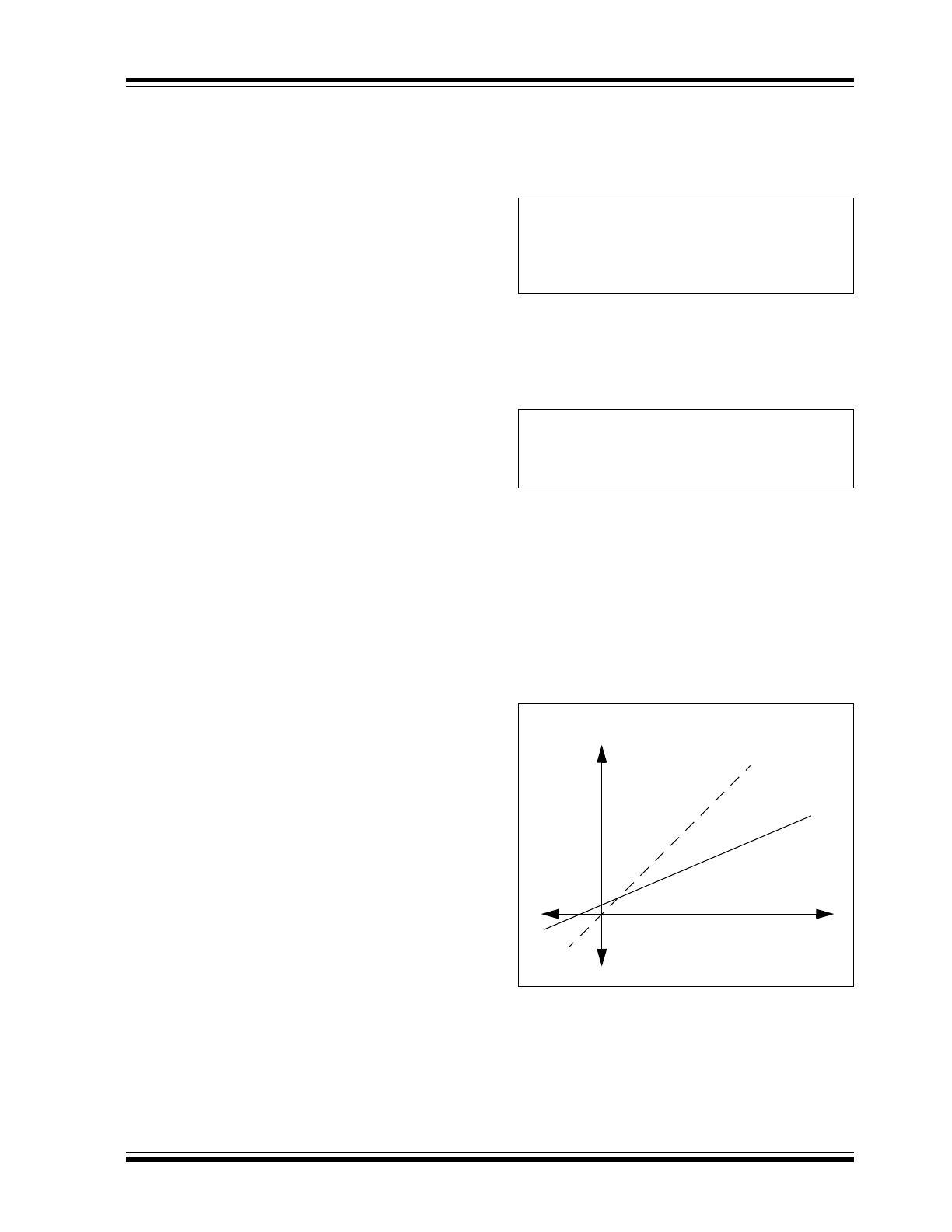
Figure 2-1 shows the relationship of the COCurr and
CFCurr values.
FIGURE 2-1:
COCurr AND CFCurr
VALUE RELATIONSHIP
9.15 mV/R
SENSE
(milliohms) = Current LSB
(Minimum current measurement if > NullCurr)
Current LSB x 16384 = Maximum Current
Measurement Possible
I(ma) = (I_A/D – COCurr – COD) * CFCurr/16384
where:
I_A/D
is the internal measurement
Ideal A/D Response
Actual A/D
Response
CFCurr
COCurr
Actual Current
Raw Measurement
PS501-0901
DS21902A-page 6
2004 Microchip Technology Inc.
2.3
Auto-Offset Compensation
Accuracy drift is prevented using an automatic auto-zero
self-calibration method, which ‘re-zeroes’ the current
measurement circuit every AOMInt * 0.5 seconds when
enabled. This feature can correct for drift in temperature
during operation. The auto-offset compensation circuit
works internally by disconnecting the RSHP and RSHN
inputs and internally shorting these inputs to measure
the zero input offset. The EEPROM and calibration
value, COD, is the true zero offset value of the particular
module.
2.4
Voltage Measurements
The A/D input channel for pack voltage measurements
is the VC(1) pin. Measurements are taken each
measurement period when the A/D is active. The
maximum voltage at the VC(1) input pin is 19V absolute,
but voltages above 18V are not suggested. The pack
voltage is measured with an integration method to
reduce any sudden spikes or fluctuations. The A/D uses
an 11-bit Resolution mode for these measurements.
The pack voltage input is read twice per measurement
period in Run mode. Voltage readings occur less
frequently in Sample mode, where A/D measurements
are not activated every measurement period, depend-
ing on the configuration of SampleLimit and NSample
values. (See Section 3.0 “Operational Modes” for
additional information.)
2.4.1
IMPEDANCE COMPENSATION
Since accurate measurement of pack voltage is critical
to performance, the voltage measurements can be
compensated for any impedance in the power path that
might affect the voltage measurements.
The EEPROM value, PackResistance, is used to
compensate for additional resistance that should be
removed.
The equation for the compensation value (in ohms) is:
EQUATION 2-3:
This requires modification of overall voltage SBData
function to compensate for pack resistance and shunt
resistance of current sense resistor. Thus, the previous
voltage equation is modified to:
EQUATION 2-4:
The voltage measurement equation is:
EQUATION 2-5:
COVPack is the “Correction Offset for Pack Voltage”
which compensates for any offset error in voltage
measurement. (Since the offset of the A/D is less than
the voltage measurement resolution of +/-16.5 mV, the
COVPack value is typically zero.)
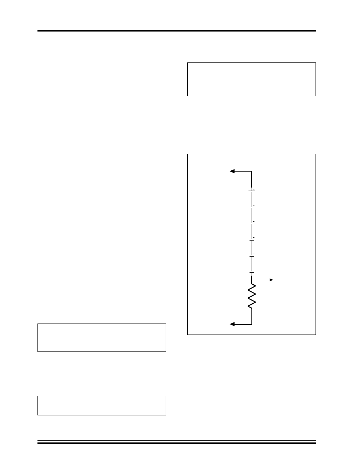
FIGURE 2-2:
PACK RESISTANCE
VALUE COMPENSATIONS
CFVPack is the “Correction Factor for Pack Voltage”
which compensates for any variance in the actual A/D
response versus an ideal A/D response over varying
voltage inputs.
PackResistance = Trace Resistance * 65535
(This is a 2-byte value, so the largest value is
1 ohm.)
SBData Voltage Value = VC(1) + Measured
Current (mA) * PackResistance/65535
V (mV) = (V_A/D – COVPack) x CFVPack/2048
where:
V_A/D
is the internal measurement output
Pack
Positive
V
SSA
Current
Sense
Resistor
Pack
Negative

2004 Microchip Technology Inc.
DS21902A-page 7
PS501-0901
The COVPack and CFVPack are calibration constants
that are stored in EEPROM.
Figure 2-3 shows the relationship of the COVPack and
CFVPack values.
FIGURE 2-3:
COVPack AND CFVPack
VALUE RELATIONSHIP
In-circuit calibration of the voltage is done at the time of
manufacture to obtain absolute accuracy in addition to
high resolution. Individual cell voltage measurements
can be accurate to within ±20 mV.
2.5
Temperature Measurements
The A/D receives input from the internal temperature
sensor to measure the temperature. Optionally, an
external thermistor can be connected to the V
NTC
pin
which is also monitored by the A/D converter. An output
reference voltage for use with an external thermistor is
provided on the V
REFT
pin. The A/D uses an 11-bit
Resolution mode for the temperature measurements.
A standard 10 kOhms at 25°C Negative-Temperature-
Coefficient (NTC) device of the 103ETB type is
suggested for the optional external thermistor. One leg
of the NTC should be connected to the V
REFT
pin and
the other to both the V
NTC
pin and a 3.65 kOhms
resistor to analog ground (V
SSA
). The resistor forms the
lower leg of a voltage divider circuit. To maintain high
accuracy in temperature measurements, a 1% resistor
should be used.
A look-up table is used to convert the voltage measure-
ment seen at the V
NTC
pin to a temperature value. The
external thermistor should be placed as close as
possible to the battery cells and should be isolated from
any other sources of heat that may affect its operation.
Calibration of the temperature measurements involves
a correction factor and an offset exactly like the current
and voltage measurements. The internal temperature
measurement makes use of correction factor CFTempI
and offset COTempI, while the V
NTC
and V
REFT
pins for
the optional external thermistor make use of correction
factor CFTempE and offset COTempE.
Ideal A/D
Actual A/D
Response
CFVPack
COVPack
A/D Output
Voltage Input
Response

PS501-0901
DS21902A-page 8
2004 Microchip Technology Inc.
3.0
OPERATIONAL MODES
The PS501-0901 operates on a continuous cycle. The
frequency of the cycles depends on the power mode
selected. There are four power modes: Run, Sample,
Sleep and Shelf-Sleep. Each mode has specific entry
and exit conditions as listed below.
3.1
Run Mode
Whether the PS501-0901 is in Run mode or Sample
mode depends on the magnitude of the current. The
Run and Sample mode entry-exit threshold is calculated
using the EEPROM parameter, SampleLimit.
SampleLimit is a programmable EEPROM value and
CFCurr is an EEPROM value set by calibration.
Entry to Run mode occurs when the current is more
than +/- SampleLimit mA for two consecutive
measurements. Run mode may only be exited to Sam-
ple mode, not to Sleep mode, when Sample mode is
enabled. Exit from Run mode to Sample mode occurs
when the converted measured current is less than the
+/- SampleLimit mA threshold for two consecutive
measurements.
Run mode is the highest power consuming mode.
During Run mode, all measurements and calculations
occur once per measurement period. Current, voltage
and temperature measurements are each typically
made sequentially during every measurement period.
3.2
Sample Mode
Entry to Sample mode occurs when the measured
current is less than +/- SampleLimit (EE parameter)
two consecutive measurements. Sample mode may be
exited to either Run mode or Sleep mode.
While in Sample mode, measurements of voltage,
current and temperature occur only once per NSample
counts of measurement periods, where NSample is a
programmable EEPROM value. Calculations of State-
Of-Charge, SMBus requests, etc. still continue at the
normal Run mode rate, but measurements only occur
once every measurement period x NSample. The
minimum value for NSample is two.
The purpose of Sample mode is to reduce power
consumption during periods of inactivity (low rate
charge or discharge). Since the analog-to-digital
converter is not active, except every NSample count of
measurement periods, the overall power consumption
is significantly reduced.
EXAMPLE 3-1:
CONFIGURATION
3.3
Low-Voltage Sleep Mode
Entry to Sleep mode can only occur when the
measured pack voltage at the VC(1) input is below a
preset limit, set by the EEPROM value SleepVPack (in
mV). Sleep mode may be exited to Run mode, but only
when one of the wake-up conditions is satisfied.
While in Sleep mode, no measurements occur and no
calculations are made. The fuel gauge display is not
operational, no SMBus communications are recog-
nized and only a wake-up condition will permit an exit
from Sleep mode. Sleep mode is one of the lowest
power consuming modes and is used to conserve
battery energy following a complete discharge.
There are two levels of Low-Voltage Sleep mode that
can be used, each with a different wake-up criteria.
Default Low-Power mode will use 25
µ
A typical and will
wake-up when the voltage exceeds the WakeUp
voltage level. By setting bit 1 of the WakeUp register to
‘
1
’, the Ultra Low-Power mode can be used. This will be
entered by low voltage, but wake-up occurs by pulling
the SMBus lines high. Ultra Low-Power mode uses less
than 1
µ
A.
3.4
Shelf-Sleep Mode
Shelf-Sleep mode is used to put the PS501-0901 into
Low-Power mode, regardless of voltage level, for long
term storage of battery packs. It is entered by an
SMBus command. It is exited by the conditions
selected in the WakeUp register. These can be voltage,
current, GPIO or SMBus activity. If any of these four are
selected for wake-up, the Shelf-Sleep mode will be
Low-Power mode and will draw 25
µ
A typical. If none of
these options are selected and bit 3 of the WakeUp
register is set, the Shelf-Sleep mode will be Ultra Low-
Power mode, which will draw less than 1
µ
A and
wake-up will be by pulling SMBus high.
Measurement period is 500 ms
SampleLimit is set to 20
NSample is set to 16
Result:
Run/Sample Mode Entry-Exit Threshold = 20 mA
During Sample mode, measurements will occur
every:
16 Measurement Periods of 500 ms = Every 8 Seconds

2004 Microchip Technology Inc.
DS21902A-page 9
PS501-0901
TABLE 3-1:
WakeUp EEPROM VALUE
TABLE 3-2:
WakeLevels EEPROM VALUE
TABLE 3-3:
POWER MODE SUMMARY
Bit
Name
Function
7
WakeIO
Wake-up from I/O Activity
6
WakeBus
Wake-up from SMBus Activity
5
WakeCurr
Wake-up from Current
4
WakeVolt
Wake-up from Voltage
3
Enable Shelf-Sleep
Use Ultra Low-Power mode for Shelf-Sleep mode. All other bits must be zero.
1
LV Sleep Mode
Use Ultra Low-Power mode as Low-Voltage Sleep mode
0
Zero Remcap
Set Remcap to zero when entering Low-Voltage Sleep mode
WakeUp Voltage (2:0)
Voltage
Purpose
000
6.4V
2 cells Li Ion
001
6.66V
6 cells NiMH
010
8.88V
8 cells NiMH
011
9.6V
3 cells Li Ion
100
9.99V
9 cells NiMH
101
11.1V
10 cells NiMH
110
12.8V
4 cells Li Ion
111
13.3V
12 cells NiMH
WakeUp Current (7:3)
Voltage
Purpose
00000
Minimum
µ
V across Sense Resistor
11000
Typical Recommended
µ
V across Sense Resistor
11111
Maximum
µ
V across Sense Resistor
Mode
Entry
Exit
Notes
Run
Measured current > preset threshold
(set by SampleLimit)
Measured current < preset threshold
(set by SampleLimit)
Highest power consumption
and accuracy for rapidly
changing current.
Sample
Measured current < preset threshold
(set by SampleLimit)
Measured current > preset threshold
(set by SampleLimit)
Saves power for low, steady
current consumption. Not as
many measurements
needed. Measurements
made every NSample
periods.
Sleep
VC(1) < SleepVPack and in
Sample mode
WakeUp voltage level exceeded
(Low-Power mode) or SMBus
pulled high (Ultra Low-Power
mode)
No measurements made.
Shelf-Sleep
SMBus command
WakeUp register conditions met
(Low-Power mode) or SMBus pins
pulled high (Ultra Low-Power
mode)
No measurements made.

PS501-0901
DS21902A-page 10
2004 Microchip Technology Inc.
4.0
CAPACITY MONITORING
The PS501-0901 internal CPU uses the voltage,
current and temperature data from the A/D converter,
along with parameters and cell models to determine the
state of the battery and to process the SBData function
instruction set.
By integrating measured current, monitoring voltages
and temperature, adjusting for self-discharge and
checking for End-Of-Charge and End-Of-Discharge
conditions, the PS501-0901 creates an accurate fuel
gauge under all battery conditions.
4.1
Capacity Calculations
The PS501-0901 calculates State-Of-Charge and fuel
gauging functions using a ‘coulomb counting’ method,
with additional inputs from battery voltage and temper-
ature measurements. By continuously and accurately
measuring all the current into and out of the battery
cells, along with accurate three-dimensional cell
models, the PS501-0901 is able to provide accurate
predictions of SOC and run time.
The capacity calculations consider two separate states:
charge acceptance or Capacity Increasing (CI) and
discharge or Capacity Decreasing (CD). The CI state
only occurs when a charge current larger than
EEPROM NullCurr value is measured. Otherwise,
while at rest and/or while being discharged, the state is
CD. Conditions must persist for at least NChangeState
measurement periods for a valid state change between
CD and CI. A minimum value of 2 is suggested for
NChangeState.
Regardless of the CI or CD state, self-discharge is also
calculated and subtracted from the integrated capacity
values. Even when charging, there is still a self-discharge
occurring in the battery.
To compensate for known system errors in the capacity
calculations, a separate error term is also continuously
calculated. This term is the basis for the SBData value
of MaxError. Two error values are located in EEPROM.
The CurrError value is the inherent error in current
measurements and should be set based on the selec-
tion of a sense resistor and calibration results. The
SelfDischrgErr value is the error in the parameter
tables for self-discharge and depends on the accuracy
of the cell chemistry model for self-discharge.
Since the PS501-0901 electronics also drain current
from the battery system, another EEPROM value allows
even this minor drain to be included in the capacity
calculations. The PwrConsumption value represents
the drain of the IC and associated circuitry, including
additional safety monitoring electronics, if present. A
typical value of 77 represents the module’s nominal
power consumption, including the PS501-0901 typical
consumption.
The total capacity added or subtracted from the battery
(change in charge) per measurement period is
expressed by the following formula:
EQUATION 4-1:
The error terms are always subtracted, even though
they are +/- errors, so that the fuel gauge value
will never be overestimated. Current draw of the
PS501-0901 and the self-discharge terms are also
always subtracted. The SBData value MaxError is the
total accumulated error as the gas gauge is running.
The battery current will be precisely measured and
integrated in order to calculate total charge removed
from or added to the battery. Based on look-up table
values, the capacity is adjusted with self-discharge
relative to current, temperature and SOC.
4.2
Discharge Termination
Discharge termination is determined based on the End-
Of-Discharge (EOD) voltage point. The voltage level at
which this point occurs can be chosen to be constant,
or to change, depending on the temperature and
discharge rate, since these factors affect the voltage
curve and total capacity of the battery. The EOD
voltage parameter table predicts the voltage point at
which this EOD will be reached, based on discharge
rate and temperature.
The PS501-0901 will monitor temperature and
discharge rate continuously and update the VEODx in
real time. When the voltage measured on the pack is
below EOD voltage for the duration of EODRecheck x
periods (500 ms), a valid EOD has occurred.
When a valid EOD has been reached, the
TERMINATE_DISCHARGE_ALARM bit (bit 11) in
BatteryStatus will be set. This will cause an
AlarmWarning condition with this bit set.
Additionally, the REMAINING_TIME_ALARM and/or
REMAINING_CAPACITY_ALARM bits can be set first
to give a user defined early warning prior to the
TERMINATE_DISCHARGE_ALARM.
The REMAINING_TIME_ALARM will trigger in
BatteryStatus when the remaining time calculation falls
below a threshold set by the SMBus command. The
REMAINING_CAPACITY_ALARM will be set in
BatteryStatus when the capacity falls below a threshold
set by the SMBus command. Use an SMBus write
command to RemainingTimeAlarm (command code
0x02) or RemainingCapacityAlarm (command code
0x01) to set these values.
∆Charge =
Σi∆t (the current integrated over time)
- CurrError (Current Measurement Error)
- PwrConsumption *
∆
t (PS501-0901 I
DD
)
- % of Self-Discharge * FCC
- SelfDischrgErr (Self-Discharge Error)