
2005 Microchip Technology Inc.
DS21927A-page 1
PS2070
Features
• Complete PS200 Battery Charger application
circuit
• Direct connection to Microchip’s PowerInfo™ 2
(PS051) interface board and PowerCal™ 2
(PS052) calibration board
• Configure PS200 with PS020 PowerTool™ 200
PC software
• Change or upgrade firmware with In-Circuit Serial
Programming™ (ICSP™)
• Evaluate charger circuits with:
- Voltage max: 16.8V
- Current max: 2.0A
• Overall mechanical dimensions:
- 2.5 W x 4.0 L (inches)
- 63.5 W x 101.6 L (millimeters)
Ordering Information
Part Number
Description
PS2070
PS200 Charger Evaluation Board and
PS020 PowerTool™ 200 Software
PS2070EV
PS2XX Charger Evaluation Board,
PS051 Configuration Interface and
PS020 PowerTool™ 200 Software
PS200 Switch Mode Charger Evaluation Board
PS2070
DS21927A-page 2
2005 Microchip Technology Inc.
1.0
PRODUCT OVERVIEW
The PS2070 evaluation board is a complete charger
evaluation circuit subsystem based on the Microchip
PS200 charge controller. The board is designed to
operate with a rechargeable battery pack consisting of
lithium based, nickel based or lead acid cells. The
board includes the Microchip PS200 battery monitor IC
in a socket, a 100 mOhm sense resistor and power
components to enable charging currents to a maximum
of 2.0A.
2.0
GENERAL SETUP
The Microchip PS2070 evaluation board plugs directly
into a PowerInfo 2 interface board or PowerCal 2
calibration board. These development tools, connected
to a PC running PowerTool™ 200 (PS020) develop-
ment software, form a complete PS200 battery charger
evaluation environment. The information that follows
will guide you through the setup of the various features
available. Please refer to the PowerInfo 2 or
PowerCal 2 data sheet for information on setting up
those products.
2.1
Connectors
• JBat – Battery input connector. The battery pack
to be charged is connected here. Looking into the
connector on the board, the pins from left to right
are:
- BAT+: Battery pack positive
- CLK:
SMBus clock
- DTA:
SMBus data
- TMP:
Temperature
- GND:
Battery pack negative
• PHost – Charger host interface. The PowerInfo 2
or PowerCal 2 is connected here. Looking into the
connector on the board, the pins from left to right
are:
- GND:
Battery pack negative
- TMP:
Temperature
- DTA:
SMBus data
- CLK:
SMBus clock
- BAT+: Battery pack positive
• J1 – In-Circuit Serial Programming (ICSP)
interface. The PS200 Flash memory can be
reprogrammed via this interface. This is only
necessary to upgrade to a newer firmware
revision or install firmware for a different
rechargeable chemistry.
• J3 – Charger DC power supply input. Input volt-
age range is 18 to 22 V
DC
. The supply must be
current limited or fused to a maximum of 2.5A.
2.2
Jumpers
• JP2 – Jumper to configure board for standard
operation with PS200 pin 2 (LED 2) connected to
the red LED or connected to PHost CLK for
communication with PowerTool 200 PC software.
• JP18 – Jumper to disconnect the overvoltage
protection divider from PS200 pin 18 (VOVP). This
allows pin 18 to be used for ICSP.
• JP19 – Jumper to disconnect the temperature
divider from PS200 pin 19 (TEMP). This allows
pin 19 to be used for ICSP.
• OPV – Jumper to configure overvoltage protection
(OVP) limit.
Jumper Position
1-2
2-3
PS200 pin 2 to Red LED
X
O
PS200 pin 2 to PHost CLK
O
X
Legend: O = open, X = connect
Jumper Position
1-2
Disable VOVP (Enable ICSP™)
O
Enable VOVP input
X
Legend: O = open, X = connect
Jumper Position
1-2
Disable TEMP (Enable ICSP™)
O
Enable TEMP input
X
Legend: O = open, X = connect
Jumper Position
1-8
(1 Cell)
2-7
(2 Cells)
3-6
(3 Cells)
4-5
(4 Cells)
OVP 4404 mV
X
O
O
O
OVP 8808 mV
O
X
O
O
OVP 13200 mV
O
O
X
O
OVP 17640 mV
O
O
O
X
No OVP limit
O
O
O
O
Legend: O = open, X = connect

2005 Microchip Technology Inc.
DS21927A-page 3
PS2070
• V
IN
– Jumper to configure voltage sense scaling
factors. The values indicate the maximum battery
voltage.
2.3
Configuration for Lithium Pack
Chemistries
Before attaching the lithium battery pack, please insure
that jumpers OVP and V
IN
are properly configured for
the maximum pack voltage. Attach the battery pack to
the JBat connector by attaching the top of the pack
(positive) to the left most pin (looking into the connec-
tor) and the bottom of the pack (negative) to the right
most pin.
2.4
Configuration for Nickel Pack
Chemistries
Rechargeable nickel based battery packs can be
attached to the PS2070. Before attaching battery cells,
please insure that jumpers OVP and V
IN
are properly
configured for the maximum pack voltage. Attach the
battery pack to the JBat connector by attaching the top
of the pack (positive) to the left most pin (looking into
the connector) and the bottom of the pack (negative) to
the right most pin.
2.5
Configuration for Lead Acid
Chemistries
Lead acid configuration will be updated when firmware
is available.
3.0
FUNCTIONAL DESCRIPTION
3.1
PS2070 Switch Mode Charger
Evaluation
The Switch Mode Charger Evaluation Board includes a
simple buck topology charger using the PS200 IC. The
PS200 monitors the battery to determine its status. The
control is a dual loop design with hardware based
current feedback control and firmware based voltage
feedback control. The hardware is configured as a
constant current loop, controlling the Pulse-Width
Modulator (PWM). The firmware sets the current level by
adjusting the PWM signal at PS200 pin 5 (CTRL
OUT
).
The firmware also measures the voltage and dynami-
cally adjusts the current to maintain the fully charged
constant voltage value. Please refer to the “PS200 Data
Sheet” for details on configuring the PS200.
Overvoltage protection – the PS200 provides
overcharge protection. This circuit can be disabled by
leaving all OVP jumper positions open. JP18 should
still be connected.
Jumper Position
1-8
(1 Cell)
2-7
(2 Cells)
3-6
(3 Cells)
4-5
(4 Cells)
5V
X
O
O
O
10V
O
X
O
O
15V
O
O
X
O
16.8V
O
O
O
X
Legend: O = open, X = connect
PS2070
DS21927A-page 4
2005 Microchip Technology Inc.
4.0
BOARD DESCRIPTION
PCB schematics and bill of materials are included here
for completeness. Schematic and Bill of Materials are
also available in the PowerTool™ 200 PC software.
4.1
Schematic
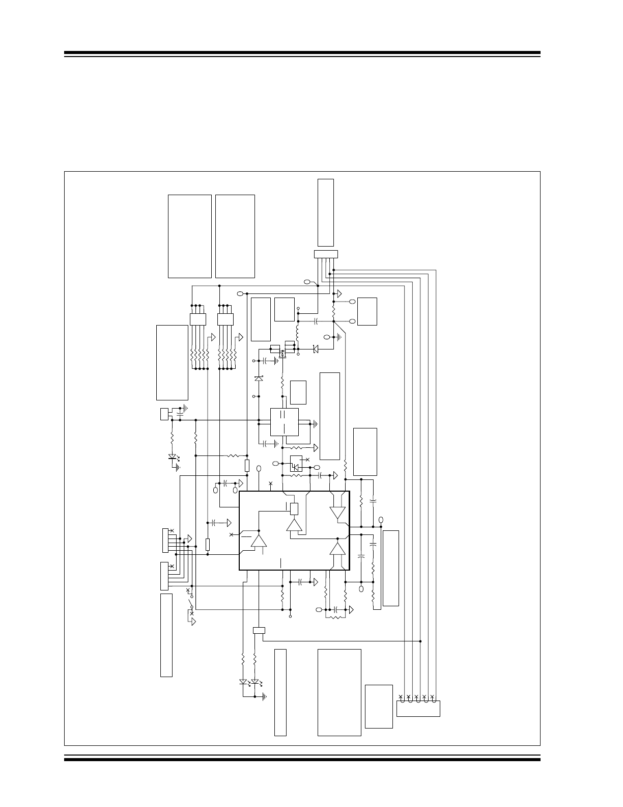
FIGURE 4-1:
PS2070 BOARD SCHEMATIC
FO
R REVI
SI
ON HI
ST
ORY,
SEE 826196 CHANGE LOG
EVALUATION/TEST BOARD FOR PS200
A1
A2
A3
A4
A5
B1
B2
B3
B4
B5
1 2 3 4 5
PHo
st
1
2
JP
19
1
2
3
4
5
6
J1
1 2 3
JP
2
V
DD
1
LE
D
2
2
V
IN
3
MCLR
4
CTRL
OUT
5
CHG
OUT
6
LOOPF
BK
7
LOOP
IN
8
CTRL
IN
9
LE
D
1
10
HV
OUT
11
I
FBINB
12
I
FBINA
13
IFB
OUT
14
BATI
D
15
CHGF
BK
16
SHDN
17
TEM
P
19
VOVP
18
V
SS
20
+
-
OP2
+
-OP1
+
-
CP2
PW
M
+
-
CP1
V
REF
S
HDN
DUT
PS
200
1
2
3
4
5
6
JP
1
R3
0
47
R4
0
0.100
BAT+
TEM
P
BAT-
V
DD
C1 100 nF
R4
1.5K
BATI
D
PGND
R1
4
19.6K
R1
3
1.00K
C8
10 nF
C7
120 nF
R7
1.27K
1 2 3 4 5
JB
at
R8
20.0K
C9 470 nF
R5 20.0K
R9 20.0K
C1
6
1.0 nF
R6 3.01K
1
2
J3
R1
62
0
R3
10
.0
K
R1
8
10
.0
K
R3
1
26
.7
K
R20
10.0K
R1
9
10.0K
1
2
JP
18
GRN LED
POW
ER
RED LED
R2
1.5K
R1
0
1.5K
R1
1
1.5K
OP
2/R
13/R
14:
CURRENT SCAL
IN
G.
SET F
O
R RANGE
OF 0-2586 mA (2.53 m
A
/B
IT
).
HARDW
ARE F
EEDBACK TO PW
M
:
OP1
IS
ERROR AMP.
R7
/R
8/
C7
/C
8 ARE
LOOP COMPENSATI
ON
COMPONENTS.
FI
RMW
ARE CURRENT-
CONTROL
OUTPUT:
CTRL
OUT
IS
COMPARE OUTPUT, W
H
ICH I
S
A F
IRM
W
A
RE
CONTROL
LE
D PW
M
THAT SETS
CURRENT L
EVEL
. R5
/R
9/
C9
SCAL
E AND
FI
LT
ER THE VOL
TAGE F
R
OM
CTRL
OUT
,
FO
R APPL
IC
ATI
ON TO OP1
.
R5
/R
9/
C9
F
O
RM
A L
O
W
-PASS F
IL
TER W
ITH A
4.
7 MI
LL
ISECOND TI
ME CONSTANT.
R
6/C
16/D
6 C
O
N
V
E
R
T 400 k
H
z P
W
M OU
TP
U
T
TO RAMP W
AVEF
ORM,
W
H
ICH I
S
F
E
D BACK
TO CP2
AND COMPARED TO ERROR AMP
SI
GNAL
TO DETERMI
NE PW
M DUTY
CY
CL
E.
POW
ER
M
O
SF
ET
DRI
VER
B
UCK
C
O
N
VER
TER
PO
W
E
R
SEC
TI
O
N
R40:
CURRE
NT
SEN
SE
R
E
SISTO
R
CHARGER DC POW
ER SUPPL
Y
IN
PUT
(W
IT
H POW
ER I
NDI
CATOR)
.
RI
GHT-
ANGL
E COMBI
CON CONNECTOR.
IN
PUT VOL
TAGE RANGE:
1
8 TO 2
2 V
DC
SUPPL
Y
MUST BE CURRENT
LI
M
ITED
OR F
U
SED AT A MAX
IMUM OF
2
.5
A
.
D2
PREVENTS
REVERSE CURRENT
W
H
EN CHARGER
IS
TURNED OF
F.
IC
SP™ I
N
TERF
ACE CONNECTORS:
OPEN JP2
AND JP5
W
H
EN USI
NG I
C
SP/
ICD.
W
H
EN BAND GAP I
S
PROPERLY
TRI
MMED,
V
DD
IS S
E
T A
T 5.000 V
DC
.
BAT
+
GN
D
CLK
DT
A
TM
P
BAT
+
GN
D
CLK
DT
A
TM
P
PowerInfo™/PowerCal™
HOST I
N
TERF
ACE
IN
VERTED
COMBI
CON
CONNECTOR
5-
PI
N RI
GHT-
ANGL
E COMBI
CON
BATTERY
IN
TERF
ACE CONNECTOR.
(M
A
TES W
ITH PSX
07
0 PCBs
)
(M
ODUL
AR)
(S
IP
)
CTRL
FD
B
K
IFB
OUT
CHG
OUT
CHGF
BK
3
1
2
D6
BAT5
4
L1
68U
H
C3 100 nF
1
2
3
4
5 6 7 8
OVP
R3
2
63
.4
K
R3
3
10
0K
R3
4
13
7K
1
2
3
4
5 6 7 8
V
IN
RST
R2
1
23
2
R2
2
10
.5
K
R2
3
20
.5
K
R2
4
30
.9
K
VOL
TAGE
SENSE SCALI
N
G F
A
CTORS:
(V
IN
HEADER)
JU
M
PER ONL
Y
ONE PI
N PAI
R AT A TI
M
E
1 C
E
LL: 4.969 mV
/B
IT
(JU
MP
E
R
1-8)
2 C
E
LL: 9.971 mV
/B
IT
(JU
MP
E
R
2-7)
3 C
E
LL: 15.01 mV
/B
IT
(JU
MP
E
R
3-6)
4 C
E
LL: 20.18 mV
/B
IT
(JU
MP
E
R
4-5)
OVP TRI
P POI
NT SEL
ECTI
ON:
(O
VP HEADER)
JU
M
PER ONL
Y
ONE PI
N PAI
R AT A TI
M
E
1 C
E
LL: 4404 mV
(JU
MP
E
R
1-8)
2 C
E
LL: 8808 mV
(JU
MP
E
R
2-7)
3 C
E
LL: 13200 mV
(JU
MP
E
R
3-6)
4 C
E
LL: 17640 mV
(JU
MP
E
R
4-5)
NO OVP -
- L
EAVE JUMPER OF
F HEADER.
D2
MB
R
S
340
C6 100 nF
C2
1
4.7
µF
C2
2
4.7
µF
C23
4.7
µF
C1
8
4.7
µF
D1
MB
RS
340
5
4
1
2
3
6
7
8
Q1 N
D
S
9435A
V
DD
1
GND
4
OUT
6
V
DD
8
GND
5
IN
2
LK
D
S
3
OUT
7
U1 TC
4431C
OA
R1
2
20.0K
PGND2
SNTP
IN
TP
PSTP
OUT
P
GND
C1
4
OPEN
VI
2005 Microchip Technology Inc.
DS21927A-page 5
PS2070
4.2
Bill of Materials
TABLE 4-1:
PS2070 BILL OF MATERIALS
Symbols
Description
Manufacturer
Manufacturer PN
Qty.
Raw PCB, PS2070
Microchip
04-826196 Rev. 2.1
1
C7
Capacitor, Ceramic, 120 nF, 25V, +/-10%,
X7R dielectric, 1206
Panasonic
ECJ-3VB1E124K
1
C9
Capacitor, Ceramic, 470 nF, 25V, +/-10%,
X7R dielectric, 1206
Murata
GRM319R71E474KA01D
1
C16
Capacitor, Ceramic, 1.0 nF, 50V, +/-10%,
X7R dielectric, 1206
Panasonic
ECU-V1H102KBM
1
C1, C3, C6
Capacitor, Ceramic, 100 nF, 50V, +/-10%,
X7R dielectric, 1206
BC Components
1206B104K500BT
3
C8
Capacitor, Ceramic, 10 nF, 50V, +/-10%,
X7R dielectric, 1206
Panasonic
ECU-V1H103KBM
1
C18,
C21-C23
Capacitor, Ceramic, 4.7
µ
F, 25V, +/-20%,
X5R dielectric, 1206
Panasonic
ECJ-3YB1E475M
4
GRNLED,
POWER
LED, clear green, 1206 package
Lumex
SML-LX1206GC-TR
2
REDLED
LED, clear red, 1206 package
Lumex
SML-LX1206SIC-TR
1
D1, D2
Schottky Diode, 40V, 3A, SMC package
On Semiconductor
International Rct.
Central Semi.
Central Semi.
MBRS340T3
MBRS340TR
CMSH3-40-PST
CMSH3-40L-PST
2
D6
Diode, Schottky, 200 mA/30V, SOT-23
Zetex
BAT54TA
1
JP2, JP18, JP19,
OVP, V
IN
Connnector, shorting jumper, female, 2-position,
100 mil spacing, mates with 25 mil square pins,
15-microinch gold over nickel.
AMP
382811-6
5
J3
Header, pluggable terminal block, 5.08 mm pitch x 2
positions, 12A/250V, right-angle, closed end
Phoenix
1757242
1
JBat
Header, pluggable terminal block, 5.08 mm pitch x 5
positions, 12A/250V, right-angle, closed end
Phoenix
1757271
1
DUT
Socket, 20-pin DIP, 0.300" spacing, machine pin
Mill-Max
110-93-320-41-001000
1
J1
Connector, modular, 6-position/6-contact,
right-angle mount
AMP
520470-3
1
BAT-, GND,
PGND, PGND2
Test point, 0.125" OD, for 0.062" hole, black
Keystone
5011
4
BAT+
Test point, 0.125" OD, for 0.062" hole, red
Keystone
5010
1
BATID, CHGFBK,
CHG
OUT
, CTRL,
FDBK, I
FBOUT
,
TEMP, VI
Test point, 0.125" OD, for 0.062" hole, white
Keystone
5012
8
L1
Inductor, 68
µ
H, 1.8A, 130 mOhms DCR,
730 x 600 mil SMT package, -40°C to +85°C
Coilcraft
DO5022P-683
1
Bumper, hemispherical, 0.44" D x 0.20" H,
transparent plastic
3M
SJ-5303 (CLEAR)
4
OVP, V
IN
Connector, break apart PCB header, straight,
2-row x 36-pin, 100 x 100 mil spacing, 235 mil/100 mil/
145 mil length, 25 mil square pins, 10-microinch gold
3M
929665-09-36-I
1
JP2, JP18, JP19
Connector, break apart PCB header, straight, 36-pin,
100 mil spacing, 235 mil/100 mil/145 mil length,
25 mil square pins, 10-microinch gold
3M
929647-09-36-I
1
J3
Pluggable terminal block, 5.08 mm pitch x 2 positions,
12A/250V
Phoenix
1757019
1
JBat
Pluggable terminal block, 5.08 mm pitch x 5 positions,
12A/250V
Phoenix
1757048
1

PS2070
DS21927A-page 6
2005 Microchip Technology Inc.
PHost
Plug, inverted Combicon, 5.08 mm pitch x 5 positions,
12A/250V
Phoenix
1786433
1
Q1
MOSFET, P-channel Enhancement mode, -30V, -5.3A,
50 mOhms, 2.5W, SO-8, -55°C to +125°C
Fairchild Semi.
NDS9435A
1
R13
Resistor, film, 1206, 1%, 1.00 kOhms
Panasonic
ERJ-8ENF1001V
1
R7
Resistor, film, 1206, 1%, 1.27 kOhms
Panasonic
ERJ-8ENF1271V
1
R3, R18-R20
Resistor, film, 1206, 1%, 10.0 kOhms
Panasonic
ERJ-8ENF1002V
4
R22
Resistor, film, 1206, 1%, 10.5 kOhms
Panasonic
ERJ-8ENF1052V
1
R33
Resistor, film, 1206, 1%, 100 kOhms
Panasonic
ERJ-8ENF1003V
1
R34
Resistor, film, 1206, 1%, 137 kOhms
Panasonic
ERJ-8ENF1373V
1
R14
Resistor, film, 1206, 1%, 19.6 kOhms
Panasonic
ERJ-8ENF1962V
1
R5, R8-R9, R12
Resistor, film, 1206, 1%, 20.0 kOhms
Panasonic
ERJ-8ENF2002V
4
R23
Resistor, film, 1206, 1%, 20.5 kOhms
Panasonic
ERJ-8ENF2052V
1
R21
Resistor, film, 1206, 1%, 232 ohms
Panasonic
ERJ-8ENF2320V
1
R31
Resistor, film, 1206, 1%, 26.7 kOhms
Panasonic
ERJ-8ENF2672V
1
R6
Resistor, film, 1206, 1%, 3.01 kOhms
Panasonic
ERJ-8ENF3011V
1
R24
Resistor, film, 1206, 1%, 30.9 kOhms
Panasonic
ERJ-8ENF3092V
1
R32
Resistor, film, 1206, 1%, 63.4 kOhms
Panasonic
ERJ-8ENF6342V
1
R2, R4, R10, R11
Resistor, film, 1206, 5%, 1.5 kOhms
Panasonic
ERJ-8GEYJ152V
4
R30
Resistor, film, 1206, 5%, 47 ohms
Panasonic
ERJ-8GEYJ470V
1
R40
Resistor, metal strip, 2512, 1%, 0.100 ohms
Vishay
WSL2512-0.100-1%-R86
1
R1
Resistor, film, 2512, 5%, 620 ohms
Panasonic
ERJ-1TYJ621U
1
RST
Switch, SPST momentary tact, surface mount,
6 mm square, 4.3 mm high, 260 G-force
E-Switch
TL3301NF260QG
1
DUT
IC, Battery Charger Microcontroller, 20-pin DIP,
-40°C to +85°C
Microchip
PS200
1
U1
IC, Power MOSFET Driver circuit, 30V, 1.5A, inverting,
with UV lockout, SO-8, 0°C to +70°C
Microchip
TC4431COA
1
TABLE 4-1:
PS2070 BILL OF MATERIALS (CONTINUED)
Symbols
Description
Manufacturer
Manufacturer PN
Qty.
2005 Microchip Technology Inc.
DS21927A-page 7
PS2070
4.3
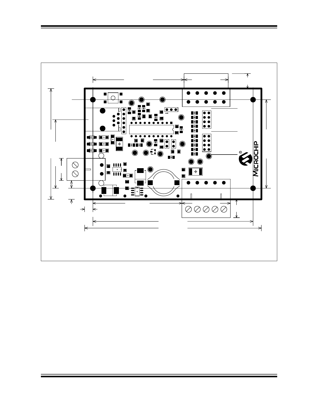
Mechanical Dimensions
Overall Dimensions: 2.5" W x 4.0" L
FIGURE 4-2:
PS2070 DIMENSION DETAILS
FOR REVISION HISTORY, REFER TO 826196 CHANGE LOG.
BODY OF J4 IS 1080 MILS WIDE,
AND OVERHANGS BOARD EDGE BY 23 MILS.
2000 (mil)
2500 (mil)
2063 (mil)
1000 (mil)
3625 (mil)
4000 (mil)
1100 (mil)
2013 (mil)
188 (mil)
250 (mil)
1548 (mil)
PHost
415 (mil)
JBat
BAT+
BAT-
OVP
V
IN
PGND
TEMP
VI
CHGFBK
PGND2
DUT
CHG
OUT
GND
FDBK
CTRL
I
FBOUT
J3
J1
175
(mil)
(J1 CENTER)
500 (mil)
PSTP
INTP
SNTP
BATID
340 (mil)
1
1
R40
C21
R21
R22
R23
R24
R3
R31
R32
R33
R34
R18
R19
JP19
C1
C18
R20
JP2
R12
C7
C3
C8
C9
C14
C16
R12
R7
JP18
L1
D6
R6
R8
R9
R5
R30
C22
C6
Q1
D1
JP1
R13
R14
OUTP
R1
R4
R10
R2
R11
C23
D2
U1
GRNLED
REDLED
POWER
RST
1
1
6
PS2070
DS21927A-page 8
2005 Microchip Technology Inc.
5.0
DEVELOPMENT TOOL
SUMMARY
Microchip provides all the necessary hardware and
software to enable easy tailoring of battery control algo-
rithm parameters and cell performance models to meet
specific application requirements and attain the highest
accuracy available anywhere. Table 5-1 summarizes
the development tool offering from Microchip to support
the PS2070. Please refer to the Microchip web site for
ordering information and design documentation
(including schematics) at www.microchip.com.
5.1
Reference Documents
This data sheet provides an overview of the PS2070
Switch Mode Charger Evaluation Board. For further
information on the PS200 and development tool opera-
tions, please refer to the following documents available
for download at www.microchip.com.
TABLE 5-1:
MICROCHIP DEVELOPMENT TOOL SUMMARY
TABLE 5-2:
MICROCHIP REFERENCE DOCUMENTS
Development Tool
Use
PowerInfo™ 2 hardware with
PowerTool™ 200 software (PS051)
Read and write register values, EEPROM programming
and test
PowerCal™ 2 hardware with
PowerTool™ 200 software (PS052)
Read and write register values, EEPROM programming, test
and calibration
Document
Number
Documents Available
DS21891
PS200 PowerSmart
®
Configurable Lithium Ion/Lithium Polymer Battery Charger Data Sheet
DS21815
PS051 PowerInfo™ 2 Configuration Interface Data Sheet
DS21817
PS052 PowerCal™ 2 Calibration Platform Data Sheet
DS21925
PS020 PowerTool™ 200 Development Software User’s Guide

2005 Microchip Technology Inc.
DS21927A-page 9
PS2070
Information contained in this publication regarding device
applications and the like is provided only for your convenience
and may be superseded by updates. It is your responsibility to
ensure that your application meets with your specifications.
MICROCHIP MAKES NO REPRESENTATIONS OR WAR-
RANTIES OF ANY KIND WHETHER EXPRESS OR IMPLIED,
WRITTEN OR ORAL, STATUTORY OR OTHERWISE,
RELATED TO THE INFORMATION, INCLUDING BUT NOT
LIMITED TO ITS CONDITION, QUALITY, PERFORMANCE,
MERCHANTABILITY OR FITNESS FOR PURPOSE.
Microchip disclaims all liability arising from this information and
its use. Use of Microchip’s products as critical components in
life support systems is not authorized except with express
written approval by Microchip. No licenses are conveyed,
implicitly or otherwise, under any Microchip intellectual property
rights.
Trademarks
The Microchip name and logo, the Microchip logo, Accuron,
K
EE
L
OQ
, MPLAB, PIC, PICmicro, PowerSmart and
SmartShunt are registered trademarks of Microchip
Technology Incorporated in the U.S.A. and other countries.
SmartSensor and The Embedded Control Solutions Company
are registered trademarks of Microchip Technology
Incorporated in the U.S.A.
PowerCal, PowerInfo, PowerMate, PowerTool, Select Mode,
Smart Serial and SmartTel are trademarks of Microchip
Technology Incorporated in the U.S.A. and other countries.
All other trademarks mentioned herein are property of their
respective companies.
© 2005, Microchip Technology Incorporated. Printed in the
U.S.A., All Rights Reserved.
Printed on recycled paper.

DS21927A-page 10
2005 Microchip Technology Inc.
AMERICAS
Corporate Office
2355 West Chandler Blvd.
Chandler, AZ 85224-6199
Tel: 480-792-7200
Fax: 480-792-7277
Technical Support:
http://support.microchip.com
Web Address:
www.microchip.com
Atlanta
Alpharetta, GA
Tel: 770-640-0034
Fax: 770-640-0307
Boston
Westford, MA
Tel: 978-692-3848
Fax: 978-692-3821
Chicago
Itasca, IL
Tel: 630-285-0071
Fax: 630-285-0075
Dallas
Addison, TX
Tel: 972-818-7423
Fax: 972-818-2924
Detroit
Farmington Hills, MI
Tel: 248-538-2250
Fax: 248-538-2260
Kokomo
Kokomo, IN
Tel: 765-864-8360
Fax: 765-864-8387
Los Angeles
Mission Viejo, CA
Tel: 949-462-9523
Fax: 949-462-9608
San Jose
Mountain View, CA
Tel: 650-215-1444
Fax: 650-961-0286
Toronto
Mississauga, Ontario,
Canada
Tel: 905-673-0699
Fax: 905-673-6509
ASIA/PACIFIC
Australia - Sydney
Tel: 61-2-9868-6733
Fax: 61-2-9868-6755
China - Beijing
Tel: 86-10-8528-2100
Fax: 86-10-8528-2104
China - Chengdu
Tel: 86-28-8676-6200
Fax: 86-28-8676-6599
China - Fuzhou
Tel: 86-591-8750-3506
Fax: 86-591-8750-3521
China - Hong Kong SAR
Tel: 852-2401-1200
Fax: 852-2401-3431
China - Shanghai
Tel: 86-21-5407-5533
Fax: 86-21-5407-5066
China - Shenyang
Tel: 86-24-2334-2829
Fax: 86-24-2334-2393
China - Shenzhen
Tel: 86-755-8203-2660
Fax: 86-755-8203-1760
China - Shunde
Tel: 86-757-2839-5507
Fax: 86-757-2839-5571
China - Qingdao
Tel: 86-532-502-7355
Fax: 86-532-502-7205
ASIA/PACIFIC
India - Bangalore
Tel: 91-80-2229-0061
Fax: 91-80-2229-0062
India - New Delhi
Tel: 91-11-5160-8631
Fax: 91-11-5160-8632
Japan - Kanagawa
Tel: 81-45-471- 6166
Fax: 81-45-471-6122
Korea - Seoul
Tel: 82-2-554-7200
Fax: 82-2-558-5932 or
82-2-558-5934
Singapore
Tel: 65-6334-8870
Fax: 65-6334-8850
Taiwan - Kaohsiung
Tel: 886-7-536-4818
Fax: 886-7-536-4803
Taiwan - Taipei
Tel: 886-2-2500-6610
Fax: 886-2-2508-0102
Taiwan - Hsinchu
Tel: 886-3-572-9526
Fax: 886-3-572-6459
EUROPE
Austria - Weis
Tel: 43-7242-2244-399
Fax: 43-7242-2244-393
Denmark - Ballerup
Tel: 45-4450-2828
Fax: 45-4485-2829
France - Massy
Tel: 33-1-69-53-63-20
Fax: 33-1-69-30-90-79
Germany - Ismaning
Tel: 49-89-627-144-0
Fax: 49-89-627-144-44
Italy - Milan
Tel: 39-0331-742611
Fax: 39-0331-466781
Netherlands - Drunen
Tel: 31-416-690399
Fax: 31-416-690340
England - Berkshire
Tel: 44-118-921-5869
Fax: 44-118-921-5820
W
ORLDWIDE
S
ALES
AND
S
ERVICE
10/20/04