

© 2008 Microchip Technology Inc.
DS21428E-page 1
TC500/A/510/514
Features:
• Precision (up to 17 bits) A/D Converter “Front
End”
• 3-Pin Control Interface to Microprocessor
• Flexible: User Can Trade-off Conversion Speed
for Resolution
• Single-Supply Operation (TC510/TC514)
• 4 Input, Differential Analog MUX (TC514)
• Automatic Input Voltage Polarity Detection
• Low Power Dissipation:
- (TC500/TC500A): 10 mW
- (TC510/TC514): 18 mW
• Wide Analog Input Range:
- ±4.2V (TC500A/TC510)
• Directly Accepts Bipolar and Differential
Input Signals
Applications:
• Precision Analog Signal Processor
• Precision Sensor Interface
• High Accuracy DC Measurements
General Description:
TheTC500/A/510/514 family are precision analog front
ends that implement dual slope A/D converters having
a maximum resolution of 17 bits plus sign. As a
minimum, each device contains the integrator, zero
crossing comparator and processor interface logic. The
TC500 is the base (16-bit max) device and requires
both positive and negative power supplies. The
TC500A is identical to the TC500 with the exception
that it has improved linearity, allowing it to operate to a
maximum resolution of 17 bits. The TC510 adds an on-
board negative power supply converter for single-
supply operation. The TC514 adds both a negative
power supply converter and a 4-input differential
analog multiplexer.
Each device has the same processor control interface
consisting of 3 wires: control inputs (A and B) and zero-
crossing comparator output (CMPTR). The processor
manipulates A, B to sequence the TC5XX through four
phases of conversion: auto-zero, integrate, de-
integrate and integrator zero. During the auto-zero
phase, offset voltages in the TC5XX are corrected by a
closed loop feedback mechanism. The input voltage is
applied to the integrator during the integrate phase.
This causes an integrator output dv/dt directly
proportional to the magnitude of the input voltage. The
higher the input voltage, the greater the magnitude of
the voltage stored on the integrator during this phase.
At the start of the de-integrate phase, an external
voltage reference is applied to the integrator and, at the
same time, the external host processor starts its on-
board timer. The processor maintains this state until a
transition occurs on the CMPTR output, at which time
the processor halts its timer. The resulting timer count
is the converted analog data. Integrator zero (the final
phase of conversion) removes any residue remaining
in the integrator in preparation for the next conversion.
The TC500/A/510/514 offer high resolution (up to
17 bits), superior 50/60 Hz noise rejection, low-power
operation, minimum I/O connections, low input bias
currents and lower cost compared to other converter
technologies having similar conversion speeds.
Precision Analog Front Ends with Dual Slope ADC
TC500/A/510/514
DS21428E-page 2
© 2008 Microchip Technology Inc.
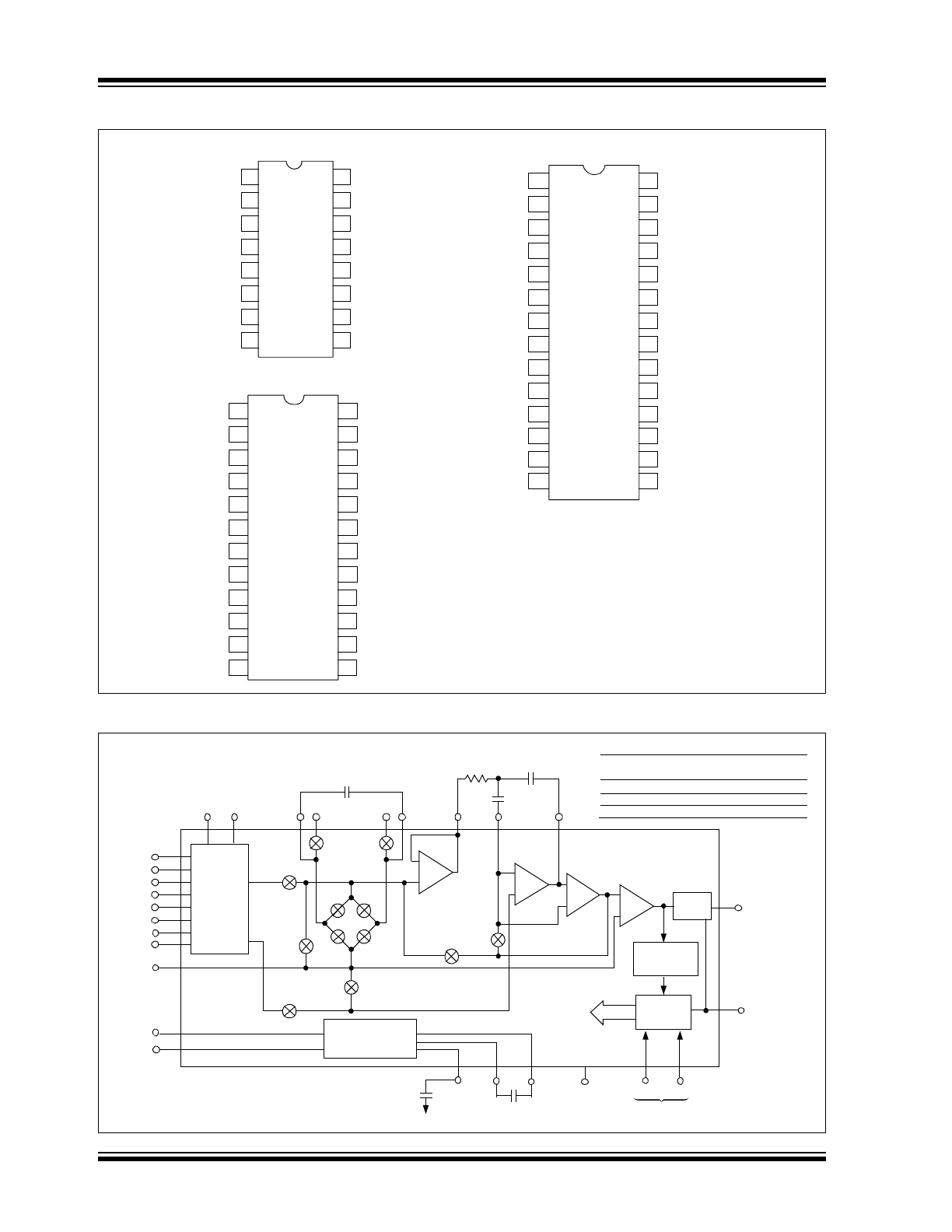
Package Types
Typical Application
1
2
3
4
16
15
14
13
5
6
7
12
11
10
9
8
CMPTR OUT
A
DGND
B
V
DD
V
IN
+
V
IN
–
V
REF
+
BUF
V
SS
C
INT
ACOM
V
REF
−
C
REF
+
C
REF
–
C
AZ
TC500/
TC500A
16-Pin PDIP/SOIC/CERDIP
V
OUT
–
1
2
3
4
20
19
18
CAP–
5
6
7
8
17
23
22
21
9
10
11
12
24
25
26
27
28
DGND
A
B
C
REF
–
C
INT
C
AZ
BUF
ACOM
CH4–
CH3–
CH2–
TC514
C
REF
+
V
REF
–
V
REF
+
V
DD
OSC
CMPTR OUT
CAP+
16
15
13
14
CH1–
N/C
CH1+
CH2+
CH3+
CH4+
A0
A1
28-Pin PDIP/SOIC
24-Pin PDIP/SOIC
1
2
3
4
16
15
14
5
6
7
8
13
19
18
17
9
10
11
12
20
21
22
23
24
TC510
CAP–
DGND
A
B
V
DD
OSC
CMPTR OUT
V
IN
+
V
IN
–
N/C
N/C
CAP+
C
REF
–
C
INT
C
AZ
BUF
ACOM
N/C
N/C
N/C
V
OUT
–
C
REF
+
V
REF
–
V
REF
+
Level
Shift
Control Logic
Analog
Switch
Control
Signals
ACOM
V
REF
+
BUF
C
AZ
Buffer
Integrator
SW
R
SW
IZ
CMPTR 1
CMPTR 2
CMPTR
Output
DGND
Control Logic
SW
1
TC500
TC500A
TC510
TC514
C
REF
C
REF
+
SW
R
C
REF
-
C
AZ
R
INT
C
INT
C
INT
SW
RI
- SW
RI
-
SW
RI
+ SW
RI
-
SW
Z
SW
I
SW
Z
V
SS
OSC
+
+
+
Phase
Decoding
Logic
Polarity
Detection
DC-TO-DC
Converter
(TC510 & TC514)
-
+
A B
0
0
Zero Integrator Output
0
1
Auto-Zero
1
0
Signal Integrate
1
1
De-integrate
V
REF
-
V
OUT
-
C
OUT
-
1.0 μF
1.0 μF
V
SS
SW
I
B
A
A0
A1
DIF.
MUX
(TC514)
CH1+
CH2+
CH3+
CH4+
CH1-
CH2-
CH3-
CH4-
CAP- CAP+
(TC500
TC500A)
Converter Sate
© 2008 Microchip Technology Inc.
DS21428E-page 3
TC500/A/510/514
1.0
ELECTRICAL
CHARACTERISTICS
Absolute Maximum Ratings†
TC510/TC514 Positive Supply Voltage
(V
DD
to GND) .........................................+10.5V
TC500/TC500A Supply Voltage
(V
DD
to V
SS
) ..............................................+18V
TC500/TC500A Positive Supply Voltage
(V
DD
to GND) ............................................+12V
TC500/TC500A Negative Supply Voltage
(V
SS
to GND)................................................-8V
Analog Input Voltage (V
IN
+ or V
IN
-) ............V
DD
to V
SS
Logic Input Voltage...............V
DD
+0.3V to GND - 0.3V
Voltage on OSC:
........................... -0.3V to (V
DD
+0.3V) for V
DD
< 5.5V
Ambient Operating Temperature Range:
................................................................ 0°C to +70°C
Storage Temperature Range:............. -65°C to +150°C
† Notice:
Stresses above those listed under “Absolute
Maximum Ratings” may cause permanent damage to
the device. These are stress ratings only and functional
operation of the device at these or any other conditions
above those indicated in the operation sections of the
specifications is not implied. Exposure to Absolute
Maximum Rating conditions for extended periods may
affect device reliability.
DC CHARACTERISTICS
Electrical Specifications:
Unless otherwise specified, TC510/TC514: V
DD
= +5V, TC500/TC500A: V
SS
= ±5V.
C
AZ
= C
REF
= 0.47
μ
F.
Parameters
Sym
T
A
= +25°C
T
A
= 0°C to 70°C
Units
Conditions
Min.
Typ.
Max.
Min.
Typ.
Max.
Analog
Resolution
60
—
—
—
—
—
μ
V
Note 1
Zero-scale Error with
Auto-zero Phase
ZSE
—
—
0.005
—
0.005
0.012
% F.S. TC500/TC510/TC514
—
—
0.003
—
0.003
0.009
TC500A
End Point Linearity
ENL
—
0.005
0.015
—
0.015
0.060
% F.S.
TC500/TC510/TC514
—
—
0.010
—
0.010
0.045
% F.S.
Note 1
, Note 2,
TC500A
Best-Case Straight
Line Linearity
NL
—
0.003
0.008
—
—
—
% F.S. TC500/TC510/TC514,
Note 1
, Note 2
—
—
0.005
—
—
—
% F.S. TC500A
Zero-scale Temp.
Coefficient
ZS
TC
—
—
—
—
1
2
μ
V/°C
Over Operating
Temperature Range
Full-scale Symmetry
Error (Rollover Error)
SYE
—
0.01
—
—
0.03
—
% F.S.
Note 1
Full-scale
Temperature
Coefficient
FS
TC
—
—
—
—
10
—
ppm/°C Over Operating
Temperature Range;
External Reference
TC = 0 ppm/°C
Input Current
I
IN
—
6
—
—
—
—
pA
V
IN
= 0V
Common Mode
Voltage Range
V
CMR
V
SS
+ 1.5
—
V
DD
– 1.5 V
SS
+ 1.5
—
V
DD
– 1.5
V
Integrator Output
Swing
V
SS
+ 0.9
—
V
DD
– 0.9 V
SS
+ 0.9
—
V
SS
+ 0.9
V
Analog Input Signal
Range
V
SS
+ 1.5
—
V
DD
– 1.5 V
SS
+ 1.5
—
V
SS
+ 1.5
V
ACOM = GND = 0V
Note
1:
Integrate time
≥ 66 ms, auto-zero time ≥ 66 ms, V
INT
(peak)
≈ 4V.
2:
End point linearity at ±1/4, ±1/2, ±3/4 F.S. after full-scale adjustment.
3:
Rollover error is related to C
INT
, C
REF
, C
AZ
characteristics.
TC500/A/510/514
DS21428E-page 4
© 2008 Microchip Technology Inc.
Voltage Reference
Range
V
REF
V
SS
+1
—
V
DD
– 1
V
SS
+1
—
V
DD
– 1
V
V
REF
-
V
REF
+
Digital
Comparator Logic 1,
Output High
V
OH
4
—
—
4
—
—
V
I
SOURCE
= 400
μ
A
Comparator Logic 0,
Output Low
V
OL
—
—
0.4
—
—
0.4
V
I
SINK
= 2.1 mA
Logic 1, Input High
Voltage
V
IH
3.5
—
—
3.5
—
—
V
Logic 0, Input Low
Voltage
V
IL
—
—
1
—
—
1
V
Logic Input Current
I
L
—
—
—
—
0.3
μ
A
Logic ‘
1
’ or ‘
0
’
Comparator Delay
t
D
—
2
—
—
3
—
μ
s
Multiplexer (TC514 Only)
Maximum Input
Voltage
-2.5
—
2.5
-2.5
—
2.5
V
V
DD
= 5V
Drain/Source ON
Resistance
R
DSON
—
6
10
—
—
—
kΩ
V
DD
= 5V
Power (TC510/TC514 Only)
Supply Current
I
S
—
1.8
2.4
—
—
3.5
mA
V
DD
= 5V, A = 1, B = 1
Power Dissipation
P
D
—
18
—
—
—
—
mW
V
DD
= 5V
Positive Supply
Operating Voltage
Range
V
DD
4.5
—
5.5
4.5 —
5.5
V
Operating Source
Resistance
R
OUT
—
60
85
—
—
100
Ω
I
OUT
= 10 mA
Oscillator Frequency
—
100
—
—
—
—
kHz
Note 1
Maximum Current
Out
I
OUT
—
—
-10
—
—
-10
mA
V
DD
= 5V
Power (TC500/TC500A Only)
Supply Current
I
S
—
1
1.5
—
—
2.5
mA
V
S
= ±5V, A = B = 1
Power Dissipation
P
D
—
10
—
—
—
—
mW
V
DD
= 5V, V
SS
= -5V
Positive Supply
Operating Range
V
DD
4.5
—
7.5
4.5 —
7.5
V
Negative Supply
Operating Range
V
SS
-4.5
—
-7.5
- 4.5
—
-7.5
V
DC CHARACTERISTICS (CONTINUED)
Electrical Specifications:
Unless otherwise specified, TC510/TC514: V
DD
= +5V, TC500/TC500A: V
SS
= ±5V.
C
AZ
= C
REF
= 0.47
μ
F.
Parameters
Sym
T
A
= +25°C
T
A
= 0°C to 70°C
Units
Conditions
Min.
Typ.
Max.
Min.
Typ.
Max.
Note
1:
Integrate time
≥ 66 ms, auto-zero time ≥ 66 ms, V
INT
(peak)
≈ 4V.
2:
End point linearity at ±1/4, ±1/2, ±3/4 F.S. after full-scale adjustment.
3:
Rollover error is related to C
INT
, C
REF
, C
AZ
characteristics.
© 2008 Microchip Technology Inc.
DS21428E-page 5
TC500/A/510/514
2.0
TYPICAL PERFORMANCE CURVES
FIGURE 2-1:
Output Voltage vs. Load
Current.
FIGURE 2-2:
Output Ripple vs. Load
Current.
FIGURE 2-3:
Oscillator Frequency vs.
Capacitance.
FIGURE 2-4:
Output Voltage vs. Output
Current.
FIGURE 2-5:
Output Source Resistance
vs. Temperature.
FIGURE 2-6:
Oscillator Frequency vs.
Temperature.
Note:
The graphs and tables provided following this note are a statistical summary based on a limited number of
samples and are provided for informational purposes only. The performance characteristics listed herein
are not tested or guaranteed. In some graphs or tables, the data presented may be outside the specified
operating range (e.g., outside specified power supply range) and therefore outside the warranted range.
Load Current (mA)
-5
-4
-3
-2
-1
0
1
2
3
4
5
0
10
20
30
40
50
60
70
80
Output Voltage (V)
T
A
= +25°C
V+ = 5V
Slope 60
Ω
Load Current (mA)
0
3
4
5
6
1
2
7
8
9 10
0
25
50
75
100
125
150
175
200
Output Ripple (mV PK-PK)
V+ = 5V, T
A
= +25°C
Osc. Freq. = 100 kHz
CAP = 1 µF
CAP = 10 µF
Oscillator Capacitance (pF)
100
10
1
1
10
100
1000
Oscillator Frequency (kHz)
T
A
= +25°C
V+ = 5V
Output Current (mA)
0
6
8
10
4
2
14
16
18
12
20
-0
-1
-3
-2
-4
-5
-7
-6
-8
Output Voltage (V)
TA = +25°C
Temperature (°C)
70
80
90
100
60
50
40
-50
0
25
-25
50
75
100
Output Source Resistance (
Ω
)
V+ = 5V
I
OUT
= 10 mA
Temperature (°C)
125
150
100
75
50
-50
0
25
-25
50
75
125
100
Oscillator Frequency (kHz)
V+ = 5V

TC500/A/510/514
DS21428E-page 6
© 2008 Microchip Technology Inc.
NOTES:
© 2008 Microchip Technology Inc.
DS21428E-page 7
TC500/A/510/514
3.0
PIN DESCRIPTIONS
The descriptions of the pins are listed in
Table 3-1
.
TABLE 3-1:
PIN FUNCTION TABLE
TC500,
TC500A
TC510
TC514
Symbol
Function
CERDIP,
PDIP, SOIC
PDIP, SOIC
PDIP, SOIC
1
2
2
C
INT
Integrator output. Integrator capacitor connection.
2
Not Used
Not Used
V
SS
Negative power supply input (TC500/TC500A only).
3
3
3
C
AZ
Auto-zero input. The auto-zero capacitor connection.
4
4
4
BUF
Buffer output. The Integrator capacitor connection.
5
5
5
ACOM
This pin is grounded in most applications. It is recommended that
ACOM and the input common pin (Ve
n
- or
CH
n
-) be within the analog
Common Mode Range (CMR).
6
6
6
C
REF
-
Input. Negative reference capacitor connection.
7
7
7
C
REF
+
Input. Positive reference capacitor connection.
8
8
8
V
REF
-
Input. External voltage reference (-) connection.
9
9
9
V
REF
+
Input. External voltage reference (+) connection.
10
15
Not Used
V
IN
-
Negative analog input.
11
16
Not Used
V
IN
+
Positive analog input.
12
18
22
A
Input. Converter phase control MSB. (See input B.)
13
17
21
B
Input. Converter phase control LSB. The states of A, B place the
TC5XX
in one of four required phases. A conversion is complete
when all four phases have been executed:
Phase control input pins: AB = 00: Integrator zero
01: Auto-zero
10: Integrate
11: De-integrate
14
19
23
CMPTR OUT Zero crossing comparator output. CMPTR is high during the
integration phase when a positive input voltage is being integrated
and is low when a negative input voltage is being integrated. A high-
to-low transition on CMPTR signals the processor that the De-
integrate phase is completed. CMPTR is undefined during the auto-
zero phase. It should be monitored to time the integrator zero phase.
15
23
27
DGND
Input. Digital ground.
16
21
25
V
DD
Input. Power supply positive connection.
—
22
26
CAP+
Input. Negative power supply converter capacitor (+) connection.
—
24
28
CAP-
Input. Negative power supply converter capacitor (-) connection.
—
1
1
V
OUT
-
Output. Negative power supply converter output and reservoir
capacitor connection. This output can be used to power other
devices in the circuit requiring a negative bias voltage.
—
20
24
OSC
Oscillator control input. The negative power supply converter
normally runs at a frequency of 100 kHz. The converter oscillator
frequency can be slowed down (to reduce quiescent current) by
connecting an external capacitor between this pin and V
DD
(see
Section 2.0 “Typical Performance Curves”
).
—
—
18
CH1+
Positive analog input pin. MUX channel 1.
—
—
13
CH1-
Negative analog input pin. MUX channel 1.
—
—
17
CH2+
Positive analog input pin. MUX channel 2.
—
—
12
CH2-
Negative analog input pin. MUX channel 2.
—
—
16
CH3+
Positive analog input pin. MUX channel 3.
—
—
11
CH3-
Negative analog input pin. MUX channel 3.
—
—
15
CH4+
Positive analog input pin. MUX channel 4.
—
—
10
CH4-
Negative analog input pin. MUX channel 4
—
—
20
A0
Multiplexer input channel select input LSB (see A1).

TC500/A/510/514
DS21428E-page 8
© 2008 Microchip Technology Inc.
—
—
19
A1
Multiplexer input channel select input MSB.
Phase control input pins: A1, A0 =
00 = Channel 1
01 = Channel 2
10 = Channel 3
11 = Channel 4
TABLE 3-1:
PIN FUNCTION TABLE (CONTINUED)
TC500,
TC500A
TC510
TC514
Symbol
Function
CERDIP,
PDIP, SOIC
PDIP, SOIC
PDIP, SOIC
© 2008 Microchip Technology Inc.
DS21428E-page 9
TC500/A/510/514
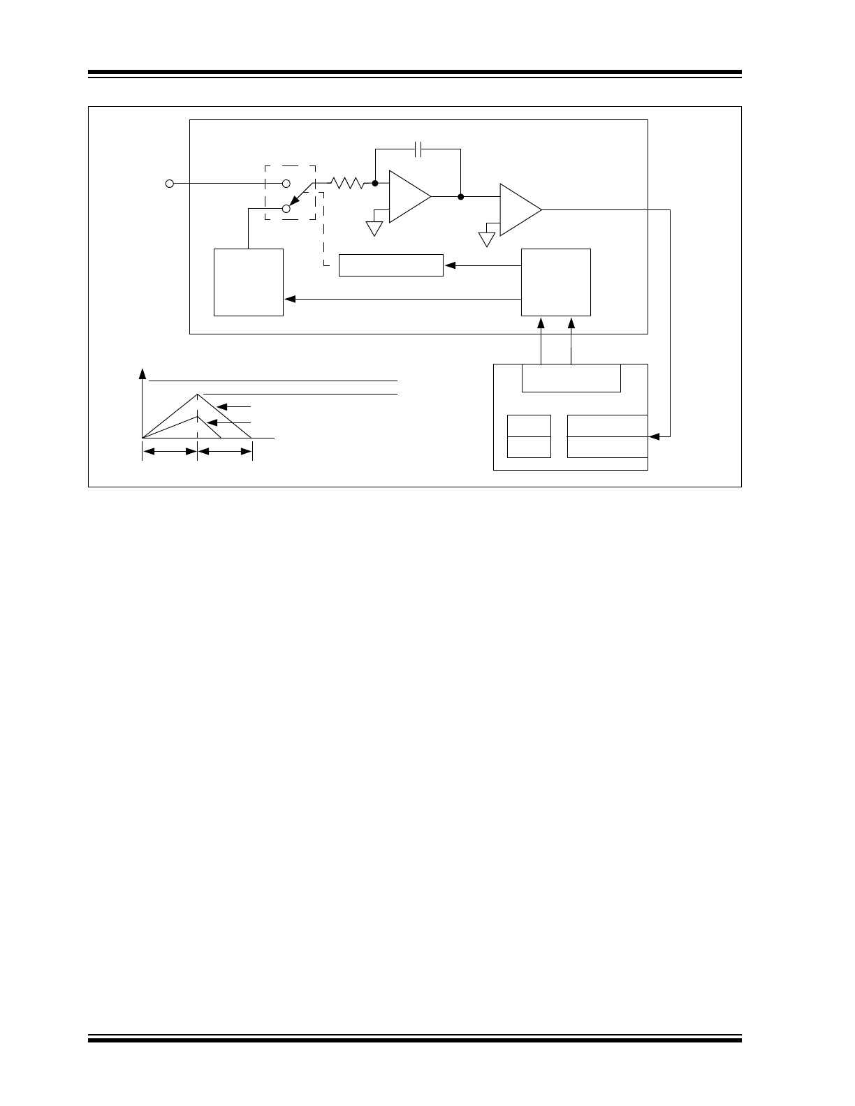
4.0
DETAILED DESCRIPTION
4.1
Dual Slope Conversion Principles
Actual data conversion is accomplished in two
phases: input signal integration and reference voltage
de-integration.
The integrator output is initialized to 0V prior to the start
of integration. During integration, analog switch S
1
connects V
IN
to the integrator input where it is
maintained for a fixed time period (T
INT
). The
application of V
IN
causes the integrator output to depart
0V at a rate determined by the magnitude of V
IN
and a
direction determined by the polarity of V
IN
. The de-
integration phase is initiated immediately at the
expiration of T
INT
.
During de-integration, S1 connects a reference voltage
(having a polarity opposite that of V
IN
) to the integrator
input. At the same time, an external precision timer is
started. The de-integration phase is maintained until
the comparator output changes state, indicating the
integrator has returned to its starting point of 0V. When
this occurs, the precision timer is stopped. The de-
integration time period (T
DEINT
), as measured by the
precision timer, is directly proportional to the magnitude
of the applied input voltage (see
Figure 4-3
).
A simple mathematical equation relates the input
signal, reference voltage and integration time:
EQUATION 4-1:
For a constant V
IN
:
EQUATION 4-2:
The dual slope converter accuracy is unrelated to the
integrating resistor and capacitor values as long as
they are stable during a measurement cycle.
An inherent benefit is noise immunity. Input noise
spikes are integrated (averaged to zero) during the
integration periods. Integrating ADCs are immune to
the large conversion errors that plague successive
approximation converters in high noise environments.
Integrating converters provide inherent noise rejection
with at least a 20dB/decade attenuation rate.
Interference signals with frequencies at integral
multiples of the integration period are, theoretically,
completely removed, since the average value of a sine
wave of frequency (1/T) averaged over a period (T) is
zero.
Integrating converters often establish the integration
period to reject 50/60 Hz line frequency interference
signals. The ability to reject such signals is shown by a
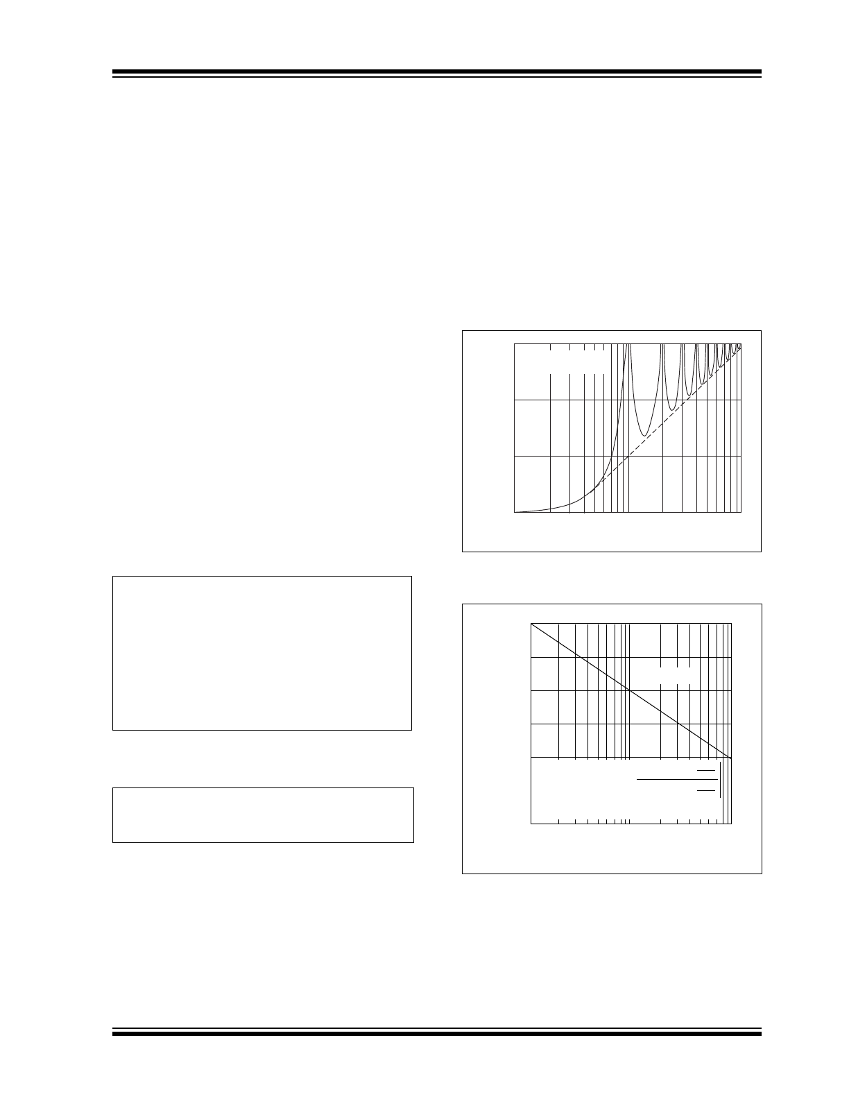
normal mode rejection plot (
Figure 4-1
). Normal mode
rejection is limited in practice to 50 to 65 dB, since the
line frequency can deviate by a few tenths of a percent
(
Figure 4-2
).
FIGURE 4-1:
Integrating Converter
Normal Mode Rejection.
FIGURE 4-2:
Line Frequency Deviation.
Where:
V
REF
=
Reference Voltage
T
INT
=
Signal Integration time (fixed)
t
DEINT
=
Reference Voltage Integration time
(variable)
1
R
INT
C
INT
------------------------
V
IN
T
( )DT
0
T
INT
∫
V
REF
C
DEINT
R
INT
C
INT
--------------------------------
=
V
IN
V
REF
T
DEINT
T
INT
------------------
=
30
20
10
0
0.1/T
1/T
10/T
Input Frequency
Normal Mode Rejection (dB)
T = Measurment
Period
0.01
0.1
1.0
Normal Mode Rejeciton (dB)
80
70
60
50
40
30
20
t = 0.1 sec
Line Frequency Deviation from 60 Hz (%)
Normal Mode = 20 LOG
Rejection
DEV = Deviation from 60 Hz
t = Integration Period
SIN 60 t (1 – )
p
p
DEV
100
DEV
100
60 t (1 – )
TC500/A/510/514
DS21428E-page 10
© 2008 Microchip Technology Inc.
FIGURE 4-3:
Basic Dual Slope Converter.
Phase
Control
Comparator
Integrator
Output
Integrator
C
INT
Analog
Input (V
IN
)
Switch Driver
Ref
Voltage
Control
Logic
Polarity Control
S
1
I/O
Timer
Counter
ROM
RAM
Microcomputer
A
B
CMPTR Out
V
SUPPLY
±
T
INT
TC510
V
INT
V
IN
≈
V
REF
V
IN
≈
1/2 V
REF
T
DEINT
–
+
R
INT
V
INT
–
+