
PL611S-02
Features
• Lowest-Power, Smallest Programmable PLL
• Very Low Jitter and Phase Noise
• Output Frequency up to:
- 110 MHz @ 1.8V Operation
- 166 MHz @ 2.5V Operation
- 200 MHz @ 3.3V Operation
• Input Frequency:
- Fundamental Crystal: 10 MHz to 50 MHz
- Reference Clock: 1 MHz to 200 MHz
• Accepts >0.1V Reference Signal Input Voltage
• One I/O Pin can be Configured as Output Enable
(OE), Frequency Switching (FSEL), Power Down
(PDB) Input, or CLK1 Output.
• <10 μA Current Consumption with PDB Active.
• Single 1.8V to 3.3V, ±10% Power Supply
• Operating Temperature Range from –40°C to
+85°C
• Available in 6-pin DFN and SOT-23
GREEN/RoHS Compliant Packages
General Description
The PL611s-02 is a low-power, small form factor, high
performance OTP-base programmable frequency
synthesizer and a part in the PicoPLL Factory
Programmable Quick Turn Clocks family.
Designed to fit in a small DFN or SOT-23 package for a
broad range of applications, the PL611s-02 offers the
best phase noise and jitter performance, and power
consumption of its rivals. In addition, one
programmable I/O pin can be configured as Output
Enable (OE), Frequency Switching (F
SEL
), Power
Down (PDB) input, or CLK1 (F
OUT
, F
REF
, F
REF
/2)
output. The power down feature of PL611s-02, when
activated, allows the IC to consume less than 10 μA of
power, while its programming flexibility allows
generating any output, up to 200 MHz using a low-cost
crystal or reference input.
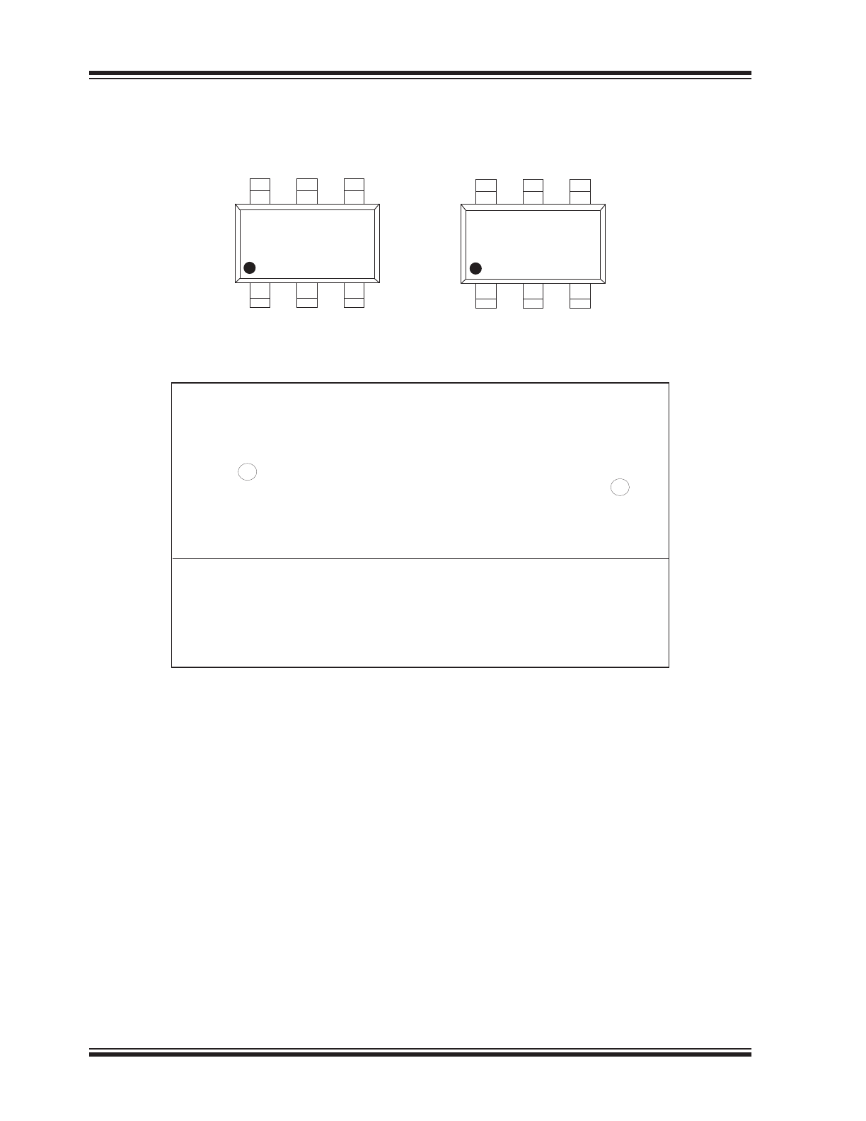
Package Types
PL611
S
-02
DFN
2.0x1.3
Top View
PL611
S
-02
SOT-23
3.0x3.0
Top View
GND
XIN, FIN
OE, PDB,
FSEL, CLK1
VDD
XOUT
CLK0
3
1
6
2
4
5
SOT-23-6
6
4
1
2
3
XIN, FIN
OE, PDB, FSEL, CLK1
GND
XOUT
5
VDD
CLK
1.8V-3.3V PicoPLL, World’s Smallest Programmable Clock
PL611S-02
DS20005670A-page 2
2016 Microchip Technology Inc.
Functional Block Diagram
Phase
Detector
Charge
Pump
Loop
Filter
VCO
XIN/FIN
XOUT
R-Counter
(8-bit)
F
VCO
= F
REF
* (2 * M/R)
F
OUT
= F
VCO
/ (2 * P)
CLK0
F
REF
OE, PDB,
FSEL, CLK1
XTAL
OSC
M-Counter
(11-bit)
Programmable
CLoad
Programmable Function
P-Counter
(5-bit)
2
1, 2
Programming
Logic

2016 Microchip Technology Inc.
DS20005670A-page 3
PL611S-02
1.0
ELECTRICAL CHARACTERISTICS
Absolute Maximum Ratings †
Supply Voltage Range, V
DD
...................................................................................................................... –0.5V to +7.0V
Input Voltage Range, V
IN
.................................................................................................................. –0.5V to V
DD
+0.5V
Output Voltage, V
OUT
........................................................................................................................ –0.5V to V
DD
+0.5V
Data Retention @ 85°C ...................................................................................................................................... 10 Years
†
Notice: Exposure of the device under conditions beyond the limits specified by Maximum Ratings for extended
periods may cause permanent damage to the device and affect product reliability. These conditions represent a stress
rating only, and functional operations of the device at these or any other conditions above the operational limits noted
in this specification is not implied. *Operating temperature is guaranteed by design. Parts are tested to commercial
grade only.
PL611S-02
DS20005670A-page 4
2016 Microchip Technology Inc.
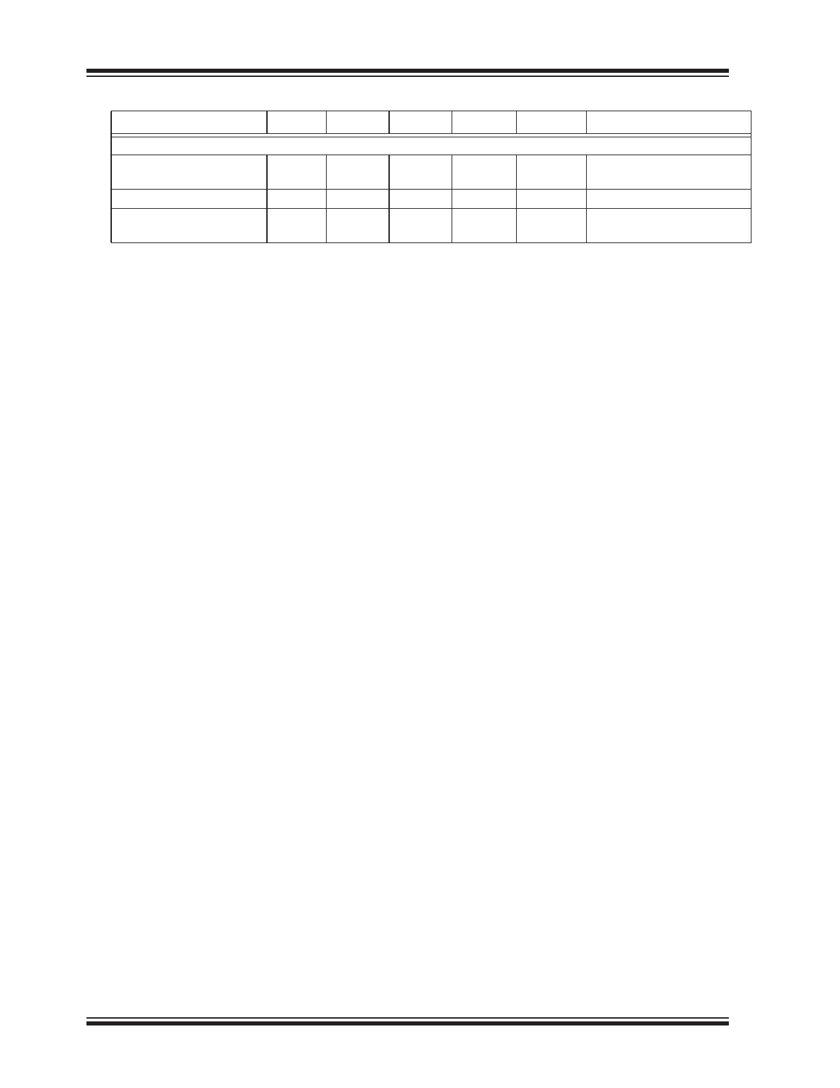
TABLE 1-1:
DC SPECIFICATIONS
Parameters
Symbol
Min.
Typ.
Max.
Units
Conditions
Supply Current, Dynamic
I
DD
—
6.0
—
mA
V
DD
= 3.3V, 30 MHz,
Load = 15 pF
—
3.9
—
V
DD
= 2.5V, 30 MHz,
Load = 15 pF
—
2.1
—
V
DD
= 1.8V, 30 MHz,
load = 15 pF
PLL Off: Supply Current,
Dynamic
I
DD
—
2.0
—
mA
V
DD
= 3.3V, 30 MHz,
Load = 15 pF
—
1.6
—
V
DD
= 2.5V, 30 MHz,
Load = 15 pF
—
0.8
—
V
DD
= 1.8V, 30 MHz,
Load = 15 pF
Supply Current, Disabled
State
I
DD
—
—
<10
μA
When PDB=0
Operating Voltage
V
DD
1.62
—
3.63
V
—
Power Supply Ramp
t
PU
0.05
—
100
ms
Time for V
DD
to reach 90%
V
DD
. Power ramp must be
monotonic.
Output Low Voltage
V
OL
—
—
0.4
V
I
OL
= +4 mA Standard Drive
Output High Voltage
V
OH
V
DD
–0.4
—
—
V
I
OH
= –4 mA Standard Drive
Output Current, Low Drive
I
OSD
4
—
—
mA
V
OL
= 0.4V, V
OH
= 2.4V
Output Current, Standard
Drive
I
OSD
8
—
—
mA
V
OL
= 0.4V, V
OH
= 2.4V
Output Current, High Drive
I
OHD
16
—
—
mA
V
OL
= 0.4V, V
OH
= 2.4V
TABLE 1-2:
AC SPECIFICATIONS
Parameters
Symbol
Min.
Typ.
Max.
Units
Conditions
Crystal Input Frequency (X
IN
)
10
—
50
MHz
Fundamental Crystal
Input (F
IN
) Frequency
1
—
200
MHz
@ V
DD
= 3.3V
1
—
166
@ V
DD
= 2.5V
1
—
110
@ V
DD
= 1.8V
Input (F
IN
) Signal Amplitude
0.9
—
V
DD
V
PP
Internally AC coupled (High
Frequency)
Input (F
IN
) Signal Amplitude
0.1
—
V
DD
V
PP
Internally AC coupled (Low
Frequency)
3.3V<50 MHz,
2.5V<40 MHz, 1.8V<15 MHz
Output Frequency
—
—
200
MHz
@ V
DD
= 3.3V
—
—
166
@ V
DD
= 2.5V
—
—
110
@ V
DD
= 1.8V
Settling Time
—
—
2
ms
At power-up (after V
DD
increases over 1.62V)
2016 Microchip Technology Inc.
DS20005670A-page 5
PL611S-02
Output Enable Time
—
—
10
ns
OE Function; T
A
=25°C,
15 pF Load. Add one
clock period to this measure-
ment for a usable
clock output.
—
—
2
ms
PDB Function; T
A
=25°C,
15 pF Load
V
DD
Sensitivity
–2
—
2
ppm
Frequency vs. V
DD
±10%
Output Rise Time
—
1.2
1.7
ns
15 pF Load, 10/90% V
DD
,
High Drive, 3.3V
Output Fall Time
—
1.2
1.7
ns
15 pF Load, 90/10% V
DD
,
High Drive, 3.3V
Duty Cycle
45
50
55
%
@2.5V and 3.3V over entire
frequency range, V
DD
/2
45
50
55
@1.8V, ≤ 75 MHz F
OUT
,
V
DD
/2
40
—
60
@1.8V, 75 MHz < F
OUT
≤
110 MHz
Period Jitter, Pk-to-Pk
(
Note 1
)
(10,000 samples measured)
—
70
—
ps
With capacitive decoupling
between V
DD
and GND
Note 1:
Jitter performance depends on the programming parameters.
TABLE 1-3:
CRYSTAL SPECIFICATIONS
Parameters
Symbol
Min
Typ
Max
Units
Fundamental Crystal Resonator Frequency
F
XIN
10
—
50
MHz
Crystal Loading Rating
(The IC can be programmed for any value in this
range)
C
L (xtal)
8
—
12
pF
Maximum Sustainable Drive Level
—
—
—
100
μW
Operating Drive Level
—
—
30
—
μW
Metal Can Crystal
Shunt Capacitance
C0
—
—
5.5
pF
ESR Max
ESR
—
—
50
Ω
Small SMD Crystal
Shunt Capacitance
C0
—
—
2.5
pF
ESR Max
ESR
—
—
80
Ω
TABLE 1-2:
AC SPECIFICATIONS (CONTINUED)
Parameters
Symbol
Min.
Typ.
Max.
Units
Conditions
PL611S-02
DS20005670A-page 6
2016 Microchip Technology Inc.
TEMPERATURE SPECIFICATIONS (
Note 1
)
Parameters
Sym.
Min.
Typ.
Max.
Units
Conditions
Temperature Ranges
Storage Temperature
Range
T
S
–65
—
150
°C
—
Soldering Temperature
T
S
—
—
260
°C
Green Package
Ambient Operating
Temperature Range
T
A
–40
—
85
°C
—
Note 1:
Exposure of the device under conditions beyond the limits specified by Maximum Ratings for extended
periods may cause permanent damage to the device and affect product reliability. These conditions repre-
sent a stress rating only, and functional operations of the device at these or any other conditions above
the operational limits noted in this specification is not implied. *Operating temperature is guaranteed by
design. Parts are tested to commercial grade only.
2016 Microchip Technology Inc.
DS20005670A-page 7
PL611S-02
2.0
PIN DESCRIPTIONS
The descriptions of the pins are listed in
Table 2-1
.
TABLE 2-1:
PIN FUNCTION TABLE
Name
Pin Assignment
Type
Description
SOT-23
DFN
OE, PDB,
FSEL,
CLK1
1
2
I/O
This programmable I/O pin can be configured as an Output
Enable (OE) input, Power Down input (PDB), On-the-Fly
Frequency Switching Selector (FSEL), or CLK1 clock output
This pin has an internal 60 kΩ pull up resistor for OE, PDB, and
FSEL.
State
OE
PDB
FSEL
0
Tri-State CLK
Power Down
Mode
Bank 1
1 (default)
Normal Mode
Normal Mode
Bank 2
GND
2
3
P
GND connection
XIN, FIN
3
1
I
Crystal or Reference Clock input pin
XOUT
4
6
O
Crystal Output pin. Do Not Connect (DNC) when F
IN
is present.
VDD
5
5
P
V
DD
connection
CLK0
6
4
O
Programmable Clock Output
TABLE 2-2:
KEY PROGRAMMING PARAMETERS
CLK[0:1]
Output Frequency
Output Drive Strength
Programmable
Input/Output
F
OUT
= F
REF
× M / (R × P)
Where:
M = 11 bit
R = 8 bit
P = 5 bit
CLK0 = F
OUT
, F
REF
or F
REF
/(2×P)
CLK1 = F
REF
, F
REF
/2, CLK0 or
CLK0/2
Three optional drive strengths to
choose from:
• Low: 4 mA
• Std: 8 mA (default)
• High: 16 mA
One output pin can be configured as:
• OE - input
• PDB - input
• FSEL - input
• CLK1 - output
PL611S-02
DS20005670A-page 8
2016 Microchip Technology Inc.
3.0
FUNCTIONAL DESCRIPTION
PL611s-02 is a highly featured, very flexible, advanced
programmable PLL design for high performance,
low-power, small form-factor applications. The
PL611s-02 accepts a fundamental input crystal of
10 MHz to 50 MHz or reference clock input of 1 MHz to
200 MHz and is capable of producing two outputs up to
200 MHz. This flexible design allows the PL611s-02 to
deliver any PLL generated frequency, F
REF
(Crystal or
REF_CLK) frequency or F
REF
/(2×P) to CLK0 and/or
CLK1. The following content explains some of the
design features of the PL611s-02.
3.1
PLL Programming
The PLL in the PL611s-02 is fully programmable. The
PLL is equipped with an 8-bit input frequency divider
(R-Counter), and an 11-bit VCO frequency feedback
loop divider (M-Counter). The output of the PLL is
transferred to a 5-bit post VCO divider (P-Counter).
The output frequency is determined by the following
formula:
EQUATION 3-1:
3.2
Clock Output (CLK0)
CLK0 is the main clock output. The output of CLK0 can
be configured as the PLL output (F
VCO
/(2×P)), F
REF
(Crystal or REF_CLK) output, or F
REF
/(2×P) output.
The output drive level can be programmed to Low Drive
(4 mA), Standard Drive (8 mA) or High Drive (16 mA).
The maximum output frequency is determined by the
Power Supply Voltage; 200 MHz at 3.3V, 166 MHz at
2.5V and 110 MHz at 1.8V.
3.3
Clock Output (CLK1)
The CLK1 feature allows the PL611s-02 to have an
additional clock output programmed to one of the
following:
• F
REF
- Reference (Crystal or REF_CLK)
Frequency
• F
REF
/ 2
• CLK0
• CLK0 / 2
3.4
Maximum VCO Frequency
For the best performance, we recommend to use the
highest VCO frequency allowed at the power supply
voltage where the PL611s-02 will be used. It is actually
the maximum VCO frequency that determines the
maximum output frequency. When a PL611s-02 is
programmed for use at a certain power supply voltage,
it is safe to use that part at higher voltages also
because at higher voltages the maximum VCO
frequency is also higher. The other way around, using
the part at a lower voltage than what it was originally
configured for, is not safe.
3.5
Output Enable (OE)
The Output Enable feature allows the user to enable
and disable the clock output(s) by toggling the OE pin.
The OE pin incorporates a 60 kΩ pull up resistor giving
a default condition of logic “1”.
3.6
Power-Down Control (PDB)
The Power Down (PDB) feature allows the user to put
the PL611s-02 into “Sleep Mode”. When activated
(logic ‘0’), PDB disables the PLL, the oscillator circuitry,
counters, and all other active circuitry. In Power Down
mode the IC consumes <10 μA of power. The PDB pin
incorporates a 60 kΩ pull up resistor giving a default
condition of logic “1”.
3.7
Frequency Select (FSEL)
The Frequency Select (FSEL) feature allows the
PL611s-02 to switch between two pre-programmed
outputs allowing the device “On the Fly” frequency
switching. The FSEL pin incorporates a 60 kΩ pull up
resistor giving a default condition of logic “1”.
F
OUT
F
REF
M
R
P
--------------------------
=
2016 Microchip Technology Inc.
DS20005670A-page 9
PL611S-02
4.0
LAYOUT RECOMMENDATIONS
The following guidelines are to assist you with a
performance optimized PCB design.
4.1
Signal Integrity and Termination
Considerations
• Keep traces short!
• Trace = Inductor. With a capacitive load this
equals ringing
• Long trace = Transmission Line. Without proper
termination this will cause reflections (looks like
ringing).
• Design long traces (greater than one inch) as
striplines or microstrips with defined impedance.
• Match trace at one side to avoid reflections
bouncing back and forth.
4.2
Decoupling and Power Supply
Considerations
• Place decoupling capacitors as close as possible
to the V
DD
pin(s) to limit noise from the power
supply
• Multiple V
DD
pins should be decoupled separately
for best performance.
• Addition of a ferrite bead in series with V
DD
can
help prevent noise from other board sources
• Value of decoupling capacitor is frequency
dependent. Typical values to use are 0.1 μF for
designs using frequencies < 50 MHz and 0.01 μF
for designs using frequencies > 50 MHz.
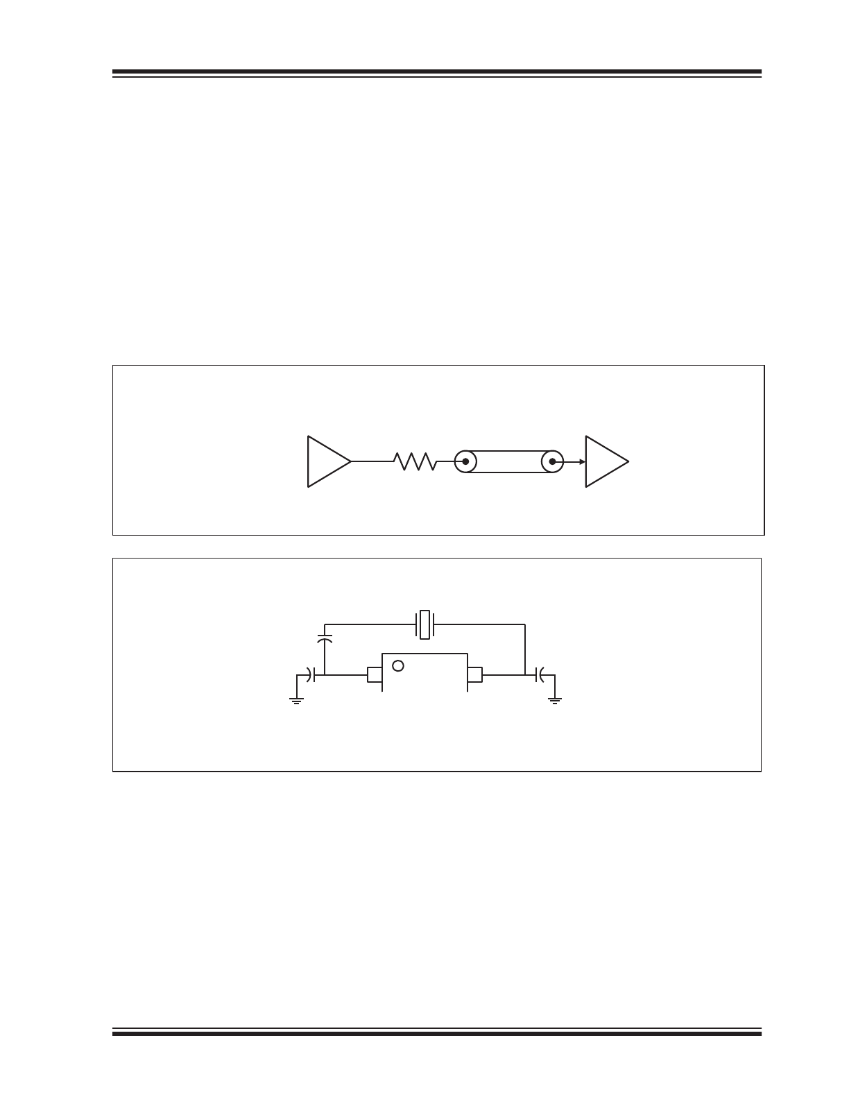
FIGURE 4-1:
Typical CMOS Termination.
FIGURE 4-2:
Crystal Tuning Circuit.
Typical CMOS Termination
Place Series Resistor as close as possible to CMOS output.
CMOS Output Buffer
(Typical buffer impedance 20Ω)
To CMOS Input
Series Resistor
Use value to match output buffer impedance
to 50Ω trace. Typical value is 30Ω.
50Ω Line
Crystal Tuning Circuit
Series and parallel capacitors used to fine tune the crystal load to the circuit load.
Crystal
XIN
1
8
XOUT
CPT
CPT
CST
CST: Series Capacitor that is used to lower circuit load to match crystal load. Raises
frequency offset. This can be eliminated by using a crystal with a C
LOAD
of equal or
greater value than the oscillator.
CPT: Parallel Capacitors that are used to raise the circuit load to match the crystal load.
Lowers frequency offset.
PL611S-02
DS20005670A-page 10
2016 Microchip Technology Inc.
5.0
PACKAGING INFORMATION
5.1
Package Marking Information
XX
XXXX-XX
NNN
YYWW
PL
611S-02
924
1610
Legend:
XX...X
Product code or customer-specific information
Y
Year code (last digit of calendar year)
YY
Year code (last 2 digits of calendar year)
WW
Week code (week of January 1 is week ‘01’)
NNN
Alphanumeric traceability code
Pb-free JEDEC
®
designator for Matte Tin (Sn)
*
This package is Pb-free. The Pb-free JEDEC designator ( )
can be found on the outer packaging for this package.
●, ▲, ▼ Pin one index is identified by a dot, delta up, or delta down (triangle
mark).
Note
:
In the event the full Microchip part number cannot be marked on one line, it will
be carried over to the next line, thus limiting the number of available
characters for customer-specific information. Package may or may not include
the corporate logo.
Underbar (_) and/or Overbar (‾) symbol may not be to scale.
3
e
3
e