
© 2009 Microchip Technology Inc.
Preliminary
DS39948A
PIC18F87J93 Family
Data Sheet
64/80-Pin, High-Performance Microcontrollers
with LCD Driver, 12-Bit A/D
and nanoWatt Technology
DS39948A-page ii
Preliminary
© 2009 Microchip Technology Inc.
Information contained in this publication regarding device
applications and the like is provided only for your convenience
and may be superseded by updates. It is your responsibility to
ensure that your application meets with your specifications.
MICROCHIP MAKES NO REPRESENTATIONS OR
WARRANTIES OF ANY KIND WHETHER EXPRESS OR
IMPLIED, WRITTEN OR ORAL, STATUTORY OR
OTHERWISE, RELATED TO THE INFORMATION,
INCLUDING BUT NOT LIMITED TO ITS CONDITION,
QUALITY, PERFORMANCE, MERCHANTABILITY OR
FITNESS FOR PURPOSE. Microchip disclaims all liability
arising from this information and its use. Use of Microchip
devices in life support and/or safety applications is entirely at
the buyer’s risk, and the buyer agrees to defend, indemnify and
hold harmless Microchip from any and all damages, claims,
suits, or expenses resulting from such use. No licenses are
conveyed, implicitly or otherwise, under any Microchip
intellectual property rights.
Trademarks
The Microchip name and logo, the Microchip logo, dsPIC,
K
EE
L
OQ
, K
EE
L
OQ
logo, MPLAB, PIC, PICmicro, PICSTART,
rfPIC and UNI/O are registered trademarks of Microchip
Technology Incorporated in the U.S.A. and other countries.
FilterLab, Hampshire, HI-TECH C, Linear Active Thermistor,
MXDEV, MXLAB, SEEVAL and The Embedded Control
Solutions Company are registered trademarks of Microchip
Technology Incorporated in the U.S.A.
Analog-for-the-Digital Age, Application Maestro, CodeGuard,
dsPICDEM, dsPICDEM.net, dsPICworks, dsSPEAK, ECAN,
ECONOMONITOR, FanSense, HI-TIDE, In-Circuit Serial
Programming, ICSP, ICEPIC, Mindi, MiWi, MPASM, MPLAB
Certified logo, MPLIB, MPLINK, mTouch, nanoWatt XLP,
Omniscient Code Generation, PICC, PICC-18, PICkit,
PICDEM, PICDEM.net, PICtail, PIC
32
logo, REAL ICE, rfLAB,
Select Mode, Total Endurance, TSHARC, WiperLock and
ZENA are trademarks of Microchip Technology Incorporated
in the U.S.A. and other countries.
SQTP is a service mark of Microchip Technology Incorporated
in the U.S.A.
All other trademarks mentioned herein are property of their
respective companies.
© 2009, Microchip Technology Incorporated, Printed in the
U.S.A., All Rights Reserved.
Printed on recycled paper.
Note the following details of the code protection feature on Microchip devices:
•
Microchip products meet the specification contained in their particular Microchip Data Sheet.
•
Microchip believes that its family of products is one of the most secure families of its kind on the market today, when used in the
intended manner and under normal conditions.
•
There are dishonest and possibly illegal methods used to breach the code protection feature. All of these methods, to our
knowledge, require using the Microchip products in a manner outside the operating specifications contained in Microchip’s Data
Sheets. Most likely, the person doing so is engaged in theft of intellectual property.
•
Microchip is willing to work with the customer who is concerned about the integrity of their code.
•
Neither Microchip nor any other semiconductor manufacturer can guarantee the security of their code. Code protection does not
mean that we are guaranteeing the product as “unbreakable.”
Code protection is constantly evolving. We at Microchip are committed to continuously improving the code protection features of our
products. Attempts to break Microchip’s code protection feature may be a violation of the Digital Millennium Copyright Act. If such acts
allow unauthorized access to your software or other copyrighted work, you may have a right to sue for relief under that Act.
Microchip received ISO/TS-16949:2002 certification for its worldwide
headquarters, design and wafer fabrication facilities in Chandler and
Tempe, Arizona; Gresham, Oregon and design centers in California
and India. The Company’s quality system processes and procedures
are for its PIC
®
MCUs and dsPIC
®
DSCs, K
EE
L
OQ
®
code hopping
devices, Serial EEPROMs, microperipherals, nonvolatile memory and
analog products. In addition, Microchip’s quality system for the design
and manufacture of development systems is ISO 9001:2000 certified.
© 2009 Microchip Technology Inc.
Preliminary
DS39948A-page 1
PIC18F87J93 FAMILY
LCD Driver and Keypad Interface
Features:
• Direct LCD Panel Drive Capability:
- Can drive LCD panel while in Sleep mode
• Up to 48 Segments and 192 Pixels, Software
Selectable
• Programmable LCD Timing module:
- Multiple LCD timing sources available
- Up to four commons: static, 1/2, 1/3 or
1/4 multiplex
- Static, 1/2 or 1/3 bias configuration
• On-Chip LCD Boost Voltage Regulator for
Contrast Control
• Charge Time Measurement Unit (CTMU) for
Capacitive Touch Sensing
• ADC for Resistive Touch Sensing
Low-Power Features:
• Power-Managed modes:
- Run: CPU On, Peripherals On
- Idle: CPU Off, Peripherals On
- Sleep: CPU Off, Peripherals Off
• Two-Speed Oscillator Start-up
Flexible Oscillator Structure:
• Two Crystal modes, 4-25 MHz
• Two External Clock modes, up to 48 MHz
• 4x Phase Lock Loop (PLL)
• Internal Oscillator Block with PLL:
- Eight user-selectable frequencies from
31.25 kHz to 8 MHz
• Secondary Oscillator using Timer1 at 32 kHz
• Fail-Safe Clock Monitor (FSCM):
- Allows for safe shutdown if peripheral clock fails
Peripheral Highlights:
• High-Current Sink/Source 25 mA/25 mA
(PORTB and PORTC)
• Up to Four External Interrupts
• Four 8-Bit/16-Bit Timer/Counter modules
• Two Capture/Compare/PWM (CCP) modules
• Master Synchronous Serial Port (MSSP) module
with Two Modes of Operation:
- 3-Wire/4-Wire SPI (supports all four SPI modes)
- I
2
C™ Master and Slave mode
• One Addressable USART module
• One Enhanced Addressable USART module:
- LIN/J2602 support
- Auto-wake-up on Start bit and Break character
- Auto-Baud Detect (ABD)
• 12-Bit, up to 12-Channel A/D Converter:
- Auto-acquisition
- Conversion available during Sleep
• Two Analog Comparators
• Programmable Reference Voltage for Comparators
• Hardware Real-Time Clock and Calendar (RTCC)
with Clock, Calendar and Alarm Functions
• Charge Time Measurement Unit (CTMU):
- Capacitance measurement
- Time measurement with 1 ns typical resolution
Note:
This document is supplemented by the
“PIC18F87J90 Family Data Sheet”
(DS39933). See Section 1.0 “Device
Overview”.
Device
Flash
Program
Memory
(Bytes)
SRAM
Data
Memory
(Bytes)
I/O
LCD
(Pixels)
T
imers
8/
16-B
it
CCP
MSSP
E
U
S
ART
AUS
ART
12-Bi
t A/D
(Ch
a
n
n
el
s)
Co
mp
arato
rs
BOR/L
V
D
RT
CC
CT
MU
SPI
Master
I
2
C™
PIC18F66J93
64K
3,923
51
132
1/3
2
Yes
Yes
1/1
12
2
Yes
Yes
Yes
PIC18F67J93
128K
3,923
51
132
1/3
2
Yes
Yes
1/1
12
2
Yes
Yes
Yes
PIC18F86J93
64K
3,923
67
192
1/3
2
Yes
Yes
1/1
12
2
Yes
Yes
Yes
PIC18F87J93
128K
3,923
67
192
1/3
2
Yes
Yes
1/1
12
2
Yes
Yes
Yes
64/80-Pin, High-Performance Microcontrollers with
LCD Driver, 12-Bit A/D and nanoWatt Technology

PIC18F87J93 FAMILY
DS39948A-page 2
Preliminary
© 2009 Microchip Technology Inc.
Special Microcontroller Features:
• 10,000 Erase/Write Cycle Flash Program
Memory, Typical
• Flash Retention 20 Years, Minimum
• Self-Programmable under Software Control
• Flash Program Memory has Word Write
Capability for Data EEPROM Emulators
• Priority Levels for Interrupts
• 8 x 8 Single-Cycle Hardware Multiplier
• Extended Watchdog Timer (WDT):
- Programmable period from 4 ms to 131s
• In-Circuit Serial Programming™ (ICSP™) via
Two Pins
• In-Circuit Debug via Two Pins
• Operating Voltage Range: 2.0V to 3.6V
• 5.5V Tolerant Input (digital pins only)
• Selectable Open-Drain Configuration for Serial
Communication and CCP Pins for Driving Outputs
up to 5V
• On-Chip 2.5V Regulator
© 2009 Microchip Technology Inc.
Preliminary
DS39948A-page 3
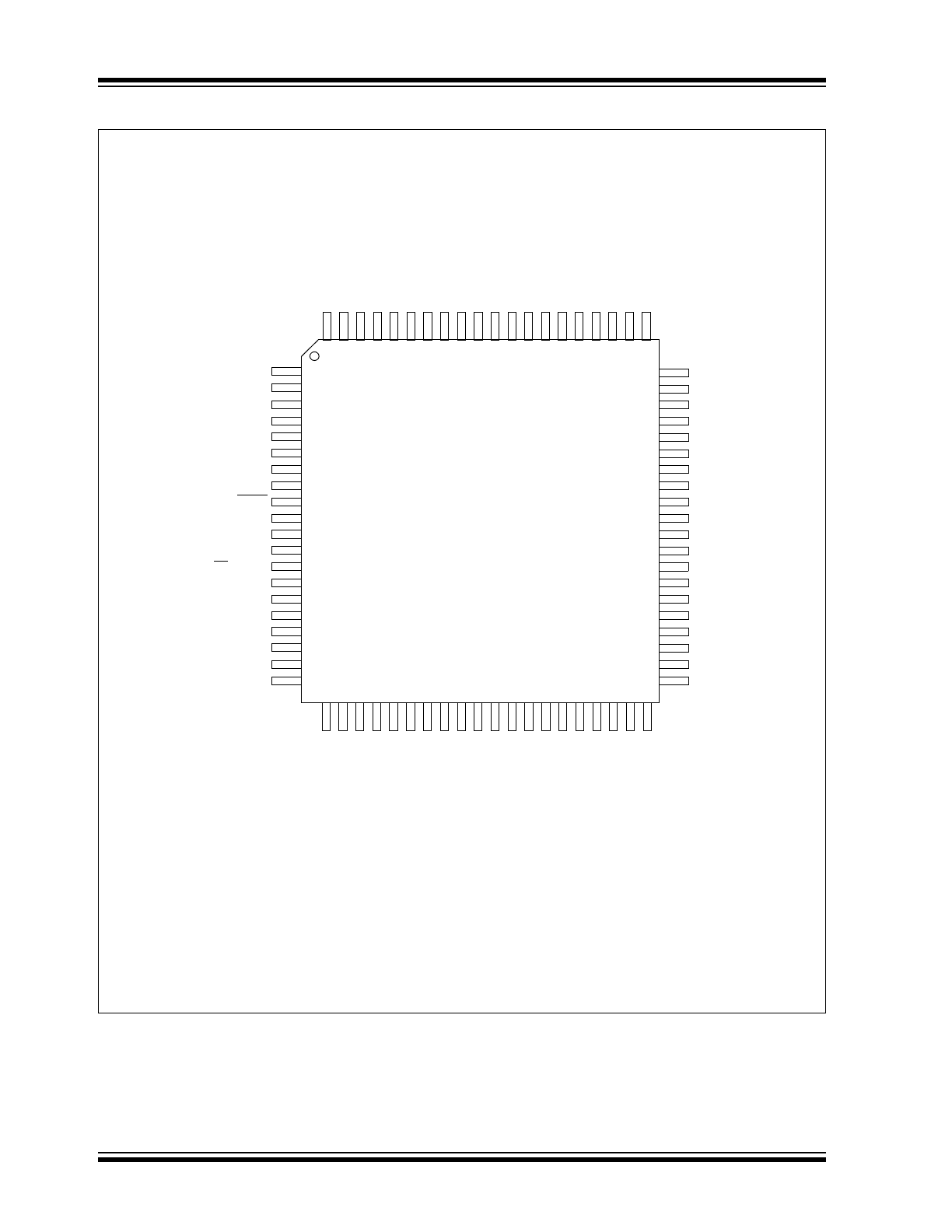
PIC18F87J93 FAMILY
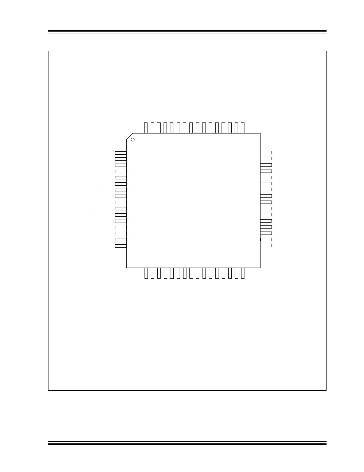
Pin Diagrams – PIC18F6XJ93
64-Pin TQFP
50 49
L
CDBIAS3
RE3
/CO
M
0
RE4
/CO
M
1
RE5
/CO
M
2
RE6
/CO
M
3
RE7
/CCP2
(1
)
/S
E
G
3
1
RD0
/SEG0
/CT
P
L
S
V
DD
V
SS
RD1
/SEG1
RD2
/SEG2
RD3
/SEG3
RD4
/SEG4
RD5
/SEG5
RD6
/SEG6
RD7
/SEG7
RE1/LCDBIAS2
RE0/LCDBIAS1
RG0/LCDBIAS0
RG1/TX2/CK2
RG2/RX2/DT2/V
LCAP
1
RG3/V
LCAP
2
MCLR
RG4/SEG26/RTCC
V
SS
V
DDCORE
/V
CAP
RF7/AN5/SS/SEG25
RF6/AN11/SEG24/C1INA
RF5/AN10/CV
REF
/SEG23/C1INB
RF4/AN9/SEG22/C2INA
RF3/AN8/SEG21/C2INB
RF2/AN7/C1OUT/SEG20
RB0/INT0/SEG30
RB1/INT1/SEG8
RB2/INT2/SEG9/CTED1
RB3/INT3/SEG10/CTED2
RB4/KBI0/SEG11
RB5/KBI1/SEG29
RB6/KBI2/PGC
V
SS
OSC2/CLKO/RA6
OSC1/CLKI/RA7
V
DD
RB7/KBI3/PGD
RC4/SDI/SDA/SEG16
RC3/SCK/SCL/SEG17
RC2/CCP1/SEG13
ENVREG
RF
1
/A
N
6
/C2
O
U
T
/S
E
G
1
9
AV
DD
AV
SS
R
A
3/A
N
3/
V
RE
F
+
RA2
/AN2
/V
RE
F
-
R
A
1/
A
N
1
/S
E
G
18
RA0
/A
N
0
V
SS
V
DD
RA4
/T
0
CKI/SEG1
4
RA5
/AN4
/SE
G
1
5
RC1
/T
1
O
SI/CCP2
(1
)
/S
E
G
32
RC0/T
1O
S
O/T
13C
K
I
RC
7
/RX1
/DT
1
/SE
G
2
8
RC6/T
X
1
/CK
1
/S
E
G
27
RC5/SDO/SEG12
54 53 52 51
58 57 56 55
60 59
64 63 62 61
Note 1:
The CCP2 pin placement depends on the CCP2MX Configuration bit setting.
PIC18F66J93
PIC18F67J93
1
2
3
4
5
6
7
8
9
10
11
12
13
14
15
16
17 18 19 20 21 22 23 24 25 26
31
27 28 29 30
32
38
37
36
35
34
33
40
39
48
47
46
45
44
43
42
41
PIC18F87J93 FAMILY
DS39948A-page 4
Preliminary
© 2009 Microchip Technology Inc.
Pin Diagrams – PIC18F8XJ93
80-Pin TQFP
3
4
5
6
7
8
9
10
11
12
13
14
15
16
48
47
46
45
44
43
42
41
40
39
64 63 62 61
21 22 23 24 25 26 27 28 29 30 31 32
L
CDBIAS3
RE3
/CO
M
0
RE4
/CO
M
1
RE5
/CO
M
2
RE6
/CO
M
3
RE7
/CCP2
(1
)
/S
E
G
3
1
RD0
/SEG0
/CT
PL
S
V
DD
V
SS
RD1
/SEG1
RD2
/SEG2
RD3
/SEG3
RD4
/SEG4
RD5
/SEG5
RD6
/SEG6
RD7
/SEG7
RE1/LCDBIAS2
RE0/LCDBIAS1
RG0/LCDBIAS0
RG1/TX2/CK2
RG2/RX2/DT2/V
LCAP
1
RG3/V
LCAP
2
MCLR
RG4/SEG26/RTCC
V
SS
V
DDCORE
/V
CAP
V
SS
OSC2/CLKO/RA6
OSC1/CLKI/RA7
V
DD
ENVRE
G
RF
1
/AN6
/C2
O
U
T/
SEG
1
9
AV
DD
AV
SS
RA3
/AN3
/V
RE
F
+
RA
2
/AN2
/V
RE
F
-
RA1
/AN1
/SEG
1
8
RA0
/AN0
V
SS
V
DD
RJ0
RJ1
/S
E
G
3
3
RH1
/SEG4
6
RH0
/SEG4
7
1
2
RH2/SEG45
RH3/SEG44
17
18
RH7/SEG43
RH6/SEG42
RH5
/SEG4
1
RH4
/SEG4
0
RJ
5
/SEG
3
8
RJ
4
/SEG
3
9
37
RJ7/SEG36
RJ6/SEG37
50
49
RJ2/SEG34
RJ3/SEG35
19
20
33 34 35 36
38
58
57
56
55
54
53
52
51
60
59
68 67 66 65
72 71 70 69
74 73
78 77 76 75
79
80
RB0/INT0/SEG30
RB1/INT1/SEG8
RB2/INT2/SEG9/CTED1
RB3/INT3/SEG10/CTED2
RB4/KBI0/SEG11
RB5/KBI1/SEG29
RB6/KBI2/PGC
RB7/KBI3/PGD
RC2/CCP1/SEG13
RC5/SDO/SEG12
RA4
/T
0
CKI/SEG1
4
RA5
/AN4
/SEG
1
5
RC1
/T
1
O
SI/CCP2
(1
)
I/
SEG
3
2
RC0
/T
1
O
SO/T
1
3
CKI
RC7/RX
1
/DT
1
/S
E
G
28
RC6/T
X
1
/C
K
1
/S
E
G
27
RF7/AN5/SS/SEG25
RF6/AN11/SEG24/C1INA
RF5/AN10/CV
REF
/SEG23/C1INB
RF4/AN9/SEG22/C2INA
RF3/AN8/SEG21/C2INB
RF2/AN7/C1OUT/SEG20
RC4/SDI/SDA/SEG16
RC3/SCK/SCL/SEG17
Note 1:
The CCP2 pin placement depends on the CCP2MX Configuration bit setting.
PIC18F86J93
PIC18F87J93

© 2009 Microchip Technology Inc.
Preliminary
DS39948A-page 5
PIC18F87J93 FAMILY
Table of Contents
1.0
Device Overview .......................................................................................................................................................................... 7
2.0
12-Bit Analog-to-Digital Converter (A/D) Module ....................................................................................................................... 27
3.0
Special Features of the CPU...................................................................................................................................................... 37
4.0
Electrical Characteristics ............................................................................................................................................................ 39
5.0
Packaging Information................................................................................................................................................................ 43
Appendix A: Revision History............................................................................................................................................................... 45
Appendix B: Device Differences .......................................................................................................................................................... 45
Appendix C: Conversion Considerations ............................................................................................................................................. 46
Appendix D: Migration From Baseline to Enhanced Devices .............................................................................................................. 46
Index .................................................................................................................................................................................................... 47
The Microchip Web Site ....................................................................................................................................................................... 49
Customer Change Notification Service ................................................................................................................................................ 49
Customer Support ................................................................................................................................................................................ 49
Reader Response ................................................................................................................................................................................ 50
Product Identification System .............................................................................................................................................................. 51

PIC18F87J93 FAMILY
DS39948A-page 6
Preliminary
© 2009 Microchip Technology Inc.
TO OUR VALUED CUSTOMERS
It is our intention to provide our valued customers with the best documentation possible to ensure successful use of your Microchip
products. To this end, we will continue to improve our publications to better suit your needs. Our publications will be refined and
enhanced as new volumes and updates are introduced.
If you have any questions or comments regarding this publication, please contact the Marketing Communications Department via
E-mail at docerrors@microchip.com or fax the Reader Response Form in the back of this data sheet to (480) 792-4150. We
welcome your feedback.
Most Current Data Sheet
To obtain the most up-to-date version of this data sheet, please register at our Worldwide Web site at:
http://www.microchip.com
You can determine the version of a data sheet by examining its literature number found on the bottom outside corner of any page.
The last character of the literature number is the version number, (e.g., DS30000A is version A of document DS30000).
Errata
An errata sheet, describing minor operational differences from the data sheet and recommended workarounds, may exist for current
devices. As device/documentation issues become known to us, we will publish an errata sheet. The errata will specify the revision
of silicon and revision of document to which it applies.
To determine if an errata sheet exists for a particular device, please check with one of the following:
• Microchip’s Worldwide Web site; http://www.microchip.com
• Your local Microchip sales office (see last page)
When contacting a sales office, please specify which device, revision of silicon and data sheet (include literature number) you are
using.
Customer Notification System
Register on our web site at www.microchip.com to receive the most current information on all of our products.

© 2009 Microchip Technology Inc.
Preliminary
DS39948A-page 7
PIC18F87J93 FAMILY
1.0
DEVICE OVERVIEW
This document contains device-specific information for
the following devices:
The PIC18F87J93 family of devices offers the
advantages of all PIC18 microcontrollers – high compu-
tational performance, a rich feature set and economical
price – with the addition of a versatile, on-chip LCD
driver. These features make the PIC18F87J93 family a
logical choice for many high-performance applications
where price is a primary consideration.
1.1
Special Features
• 12-Bit A/D Converter: The PIC18F87J93 family
implements a 12-bit A/D converter. A/D converters
in both families incorporate programmable acquisi-
tion time. This allows for a channel to be selected
and a conversion to be initiated, without waiting for
a sampling period and thus, reducing code
overhead.
• Data RAM: The PIC18F87J93 family devices have
3,923 bytes of RAM.
1.2
Details on Individual Family
Members
Devices in the PIC18F87J93 family are available in
64-pin and 80-pin packages. Block diagrams for the
two groups are shown in Figure 1-1 and Figure 1-2.
The devices are differentiated from each other in the
following ways:
• Flash Program Memory (64 Kbytes for
PIC18FX6J93 devices and 128 Kbytes for
PIC18FX7J93).
• LCD Pixels:
- 64-pin devices – 132 pixels
(33 SEGs x 4 COMs)
- 80-pin devices – 192 pixels
(48 SEGs x 4 COMs)
• I/O Ports (seven bidirectional ports on
PIC18F6XJ93 devices and nine bidirectional ports
on PIC18F8XJ93 devices).
All other features for devices in this family are identical
and are summarized in Table 1-1 and Table 1-2.
The devices’ block diagrams are given in Figure 1-1
and Figure 1-2.
The pinouts for all devices are listed in Table 1-3 and
Table 1-4.
• PIC18F66J93
• PIC18F67J93
• PIC18F86J93
• PIC18F87J93
Note: This data sheet documents only the devices’
features and specifications that are in addition
to the features and specifications of the
PIC18F87J90 family devices. For information
on the features and specifications shared by
the PIC18F87J93 family and PIC18F87J90
family devices, see the “PIC18F87J90 Family
Data Sheet” (DS39933).
PIC18F87J93 FAMILY
DS39948A-page 8
Preliminary
© 2009 Microchip Technology Inc.
TABLE 1-1:
DEVICE FEATURES FOR THE PIC18F6XJ93 (64-PIN DEVICES)
TABLE 1-2:
DEVICE FEATURES FOR THE PIC18F8XJ93 (80-PIN DEVICES)
Features
PIC18F66J93
PIC18F67J93
Operating Frequency
DC – 48 MHz
Program Memory (Bytes)
64K
128K
Program Memory (Instructions)
32,768
65,536
Data Memory (Bytes)
3,923
3,923
Interrupt Sources
29
I/O Ports
Ports A, B, C, D, E, F, G
LCD Driver (available pixels to drive)
132 (33 SEGs x 4 COMs)
Timers
4
Comparators
2
CTMU
Yes
RTCC
Yes
Capture/Compare/PWM Modules
2
Serial Communications
MSSP, Addressable USART, Enhanced USART
12-Bit Analog-to-Digital Module
12 Input Channels
Resets (and Delays)
POR, BOR, RESET Instruction, Stack Full, Stack Underflow, MCLR, WDT
(PWRT, OST)
Instruction Set
75 Instructions, 83 with Extended Instruction Set Enabled
Packages
64-Pin TQFP
Features
PIC18F86J93
PIC18F87J93
Operating Frequency
DC – 48 MHz
Program Memory (Bytes)
64K
128K
Program Memory (Instructions)
32,768
65,536
Data Memory (Bytes)
3,923
3,923
Interrupt Sources
29
I/O Ports
Ports A, B, C, D, E, F, G, H, J
LCD Driver (available pixels to drive)
192 (48 SEGs x 4 COMs)
Timers
4
Comparators
2
CTMU
Yes
RTCC
Yes
Capture/Compare/PWM Modules
2
Serial Communications
MSSP, Addressable USART, Enhanced USART
12-Bit Analog-to-Digital Module
12 Input Channels
Resets (and Delays)
POR, BOR, RESET Instruction, Stack Full, Stack Underflow, MCLR, WDT
(PWRT, OST)
Instruction Set
75 Instructions, 83 with Extended Instruction Set Enabled
Packages
80-Pin TQFP