
2012 Microchip Technology Inc.
DS30509A-page 1
High-Temperature Features:
• Ambient Temperature Range of -40°C to +150°C
Power-Managed Modes:
• Run: CPU on, Peripherals on
• Idle: CPU off, Peripherals on
• Sleep: CPU off, Peripherals off
• Two-Speed Oscillator Start-up
• Fail-Safe Clock Monitor (FSCM)
• Power-Saving Peripheral Module Disable (PMD)
• Ultra Low-Power Wake-up
• Fast Wake-up, 1 µs, Typical
• Low-Power WDT, 300 nA, Typical
• Run mode Currents Down to Very Low 3.8 µA,
Typical
• Idle mode Currents Down to Very Low 880 nA,
Typical
• Sleep mode Currents Down to Very Low 13 nA,
Typical
ECAN Bus Module Features:
• Conforms to CAN 2.0B Active Specification
• Three Operating modes:
- Legacy mode (full backward compatibility with
existing PIC18CXX8/FXX8 CAN modules)
- Enhanced mode
- FIFO mode or programmable TX/RX buffers
• Message Bit Rates up to 1 Mbps
• DeviceNet™ Data Byte Filter Support
ECAN Bus Module Features (Continued):
• Six Programmable Receive/Transmit Buffers
• Three Dedicated Transmit Buffers with Prioritiza-
tion
• Two Dedicated Receive Buffers
• 16 Full, 29-Bit Acceptance Filters with Dynamic
Association
• Three Full, 29-Bit Acceptance Masks
• Automatic Remote Frame Handling
• Advanced Error Management Features
Special Microcontroller Features:
• On-Chip 3.3V Regulator
• Operating Speed up to 64 MHz
• 3.6 Kbytes of General Purpose Registers (SRAM)
• Three Internal Oscillators:
- LF-INTOSC (31 kHz)
- MF-INTOSC (500 kHz)
- HF-INTOSC (16 MHz)
• Priority Levels for Interrupts
• 8 x 8 Single-Cycle Hardware Multiplier
• Extended Watchdog Timer (WDT):
- Programmable period from 4 ms to 4,194s
• In-Circuit Serial Programming™ (ICSP™) via Two
Pins
• In-Circuit Debug via Two Pins
• Programmable BOR
• Programmable LVD
TABLE 1:
DEVICE COMPARISON
Device
Program
Memory
Data
Memory
(Bytes)
Data
EE
(Bytes)
Pins
I/O
CTMU
1
2
-Bi
t A/
D
Cha
n
n
e
ls
CCP
/
ECCP
Ti
m
e
rs
8-
B
it
/16-
B
it
EUSAR
T
C
o
mp
arat
ors
E
CAN™
MS
S
P
BOR
M
V/
L
V
D
DSM
PIC18F25K80
32 Bytes
3,648
1,024
28
24
1
8-ch
4/1
2/3
2
2
1
1
Yes
No
PIC18F26K80
64 Bytes
3,648
1,024
28
24
1
8-ch
4/1
2/3
2
2
1
1
Yes
No
PIC18F45K80
32 Bytes
3,648
1,024
40/44
35
1
11-ch
4/1
2/3
2
2
1
1
Yes
No
PIC18F46K80
64 Bytes
3,648
1,024
40/44
35
1
11-ch
4/1
2/3
2
2
1
1
Yes
No
PIC18F65K80
32 Bytes
3,648
1,024
64
54
1
11-ch
4/1
2/3
2
2
1
1
Yes
Yes
PIC18F66K80
64 Bytes
3,648
1,024
64
54
1
11-ch
4/1
2/3
2
2
1
1
Yes
Yes
PIC18F66K80 FAMILY
28/40/44/64-Pin, High-Temperature, Enhanced Flash
Microcontrollers with ECAN
™
and nanoWatt XLP Technology

PIC18F66K80 FAMILY
DS30509A-page 2
2012 Microchip Technology Inc.
Peripheral Highlights:
• Five CCP/ECCP modules:
- Four Capture/Compare/PWM (CCP) modules
- One Enhanced Capture/Compare/PWM
(ECCP) module
• Five 8/16-Bit Timer/Counter modules:
- Timer0: 8/16-bit timer/counter with 8-bit
programmable prescaler
- Timer1, Timer3: 16-bit timer/counter
- Timer2, Timer4: 8-bit timer/counter
• Two Analog Comparators
• Configurable Reference Clock Output
• Charge Time Measurement Unit (CTMU):
- Capacitance measurement
- Time measurement with 1 ns typical resolution
- Integrated voltage reference
• Up to Four External Interrupts
• One Master Synchronous Serial Port
(MSSP) module:
- 3/4-wire SPI (supports all four SPI modes)
- I
2
C™ Master and Slave modes
• Two Enhanced Addressable USART modules:
- LIN/J2602 support
- Auto-Baud Detect (ABD)
• 12-Bit A/D Converter with up to 11 Channels:
- Auto-acquisition and Sleep operation
- Differential Input mode of operation
• Data Signal Modulator module:
- Select modulator and carrier sources from
various module outputs
• Integrated Voltage Reference

2012 Microchip Technology Inc.
DS30509A-page 3
PIC18F66K80 FAMILY
Table of Contents
1.0
Device Overview .......................................................................................................................................................................... 5
2.0
Special Features of the CPU........................................................................................................................................................ 7
3.0
Electrical Characteristics .............................................................................................................................................................. 9
Appendix A: Revision History............................................................................................................................................................... 13
The Microchip Web Site....................................................................................................................................................................... 15
Customer Change Notification Service ................................................................................................................................................ 15
Customer Support................................................................................................................................................................................ 15
Reader Response ................................................................................................................................................................................ 16
Product Identification System .............................................................................................................................................................. 17

PIC18F66K80 FAMILY
DS30509A-page 4
2012 Microchip Technology Inc.
TO OUR VALUED CUSTOMERS
It is our intention to provide our valued customers with the best documentation possible to ensure successful use of your Microchip
products. To this end, we will continue to improve our publications to better suit your needs. Our publications will be refined and
enhanced as new volumes and updates are introduced.
If you have any questions or comments regarding this publication, please contact the Marketing Communications Department via
E-mail at docerrors@microchip.com or fax the Reader Response Form in the back of this data sheet to (480) 792-4150. We
welcome your feedback.
Most Current Data Sheet
To obtain the most up-to-date version of this data sheet, please register at our Worldwide Web site at:
http://www.microchip.com
You can determine the version of a data sheet by examining its literature number found on the bottom outside corner of any page.
The last character of the literature number is the version number, (e.g., DS30000A is version A of document DS30000).
Errata
An errata sheet, describing minor operational differences from the data sheet and recommended workarounds, may exist for current
devices. As device/documentation issues become known to us, we will publish an errata sheet. The errata will specify the revision
of silicon and revision of document to which it applies.
To determine if an errata sheet exists for a particular device, please check with one of the following:
• Microchip’s Worldwide Web site; http://www.microchip.com
• Your local Microchip sales office (see last page)
When contacting a sales office, please specify which device, revision of silicon and data sheet (include literature number) you are
using.
Customer Notification System
Register on our web site at www.microchip.com to receive the most current information on all of our products.

2012 Microchip Technology Inc.
DS30509A-page 5
PIC18F66K80 FAMILY
1.0
DEVICE OVERVIEW
This document contains device-specific information for
the following devices, operating in an ambient
temperature range between -40°C and +150°C:
This family of devices offers the advantages of all
PIC18 microcontrollers; namely, high computational
performance at an economical price. In addition to these
features, the PIC18F66K80 family introduces design
enhancements that make these microcontrollers a logical
choice for many high-performance, power-sensitive
applications.
The primary differentiating features and specifications
of the high-temperature PIC18F66K80 family devices
are:
• Above +125°C, writes are not allowed for Flash
program memory
• All AC timing specifications are increased by 15%
This derating factor includes parameters, such as
T
PWRT
• Maximum HS frequency of operation is 64 MHz
• PIC18F25K80
• PIC18F46K80
• PIC18F26K80
• PIC18F65K80
• PIC18F45K80
• PIC18F66K80
Note:
This data sheet documents only the devices’
features and specifications that are in
addition to the features and specifications of
the non-specialty PIC18F66K80 devices.
For information on the features and
specifications shared by this document’s high-
temperature devices and the non-specialty
devices, see the “PIC18F66K80 Family Data
Sheet”
(DS39977).
Note:
The test duration for AEC-Q100 reliability
testing for devices operating at +150°C is
1,000 hours. Any design operating at
+125°C to +150°C for longer than that
period is not warranted without prior written
approval from Microchip Technology Inc.

PIC18F66K80 FAMILY
DS30509A-page 6
2012 Microchip Technology Inc.
NOTES:
2012 Microchip Technology Inc.
DS30509A-page 7
PIC18F66K80 FAMILY
2.0
SPECIAL FEATURES OF THE
CPU
2.1
Device ID Registers
The Device ID registers are read-only registers. They
identify the device type and revision for device
programmers and can be read by firmware using table
reads.
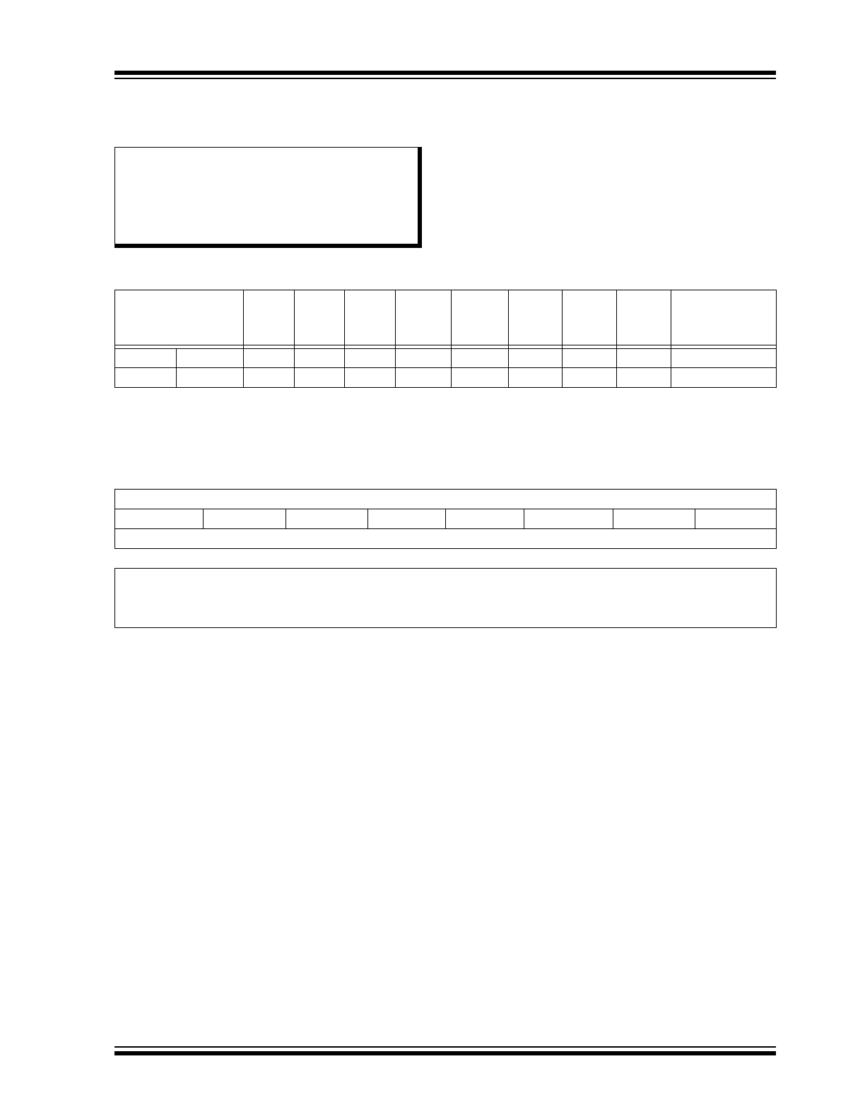
TABLE 2-1:
DEVICE IDs
Note:
For additional details on the Configuration bits,
refer to Section 28.1 “Configuration Bits” in
the “PIC18F66K80 Family Data Sheet”
(DS39977). Device ID information presented in
this section is for the high-temperature
PIC18F66K80 family devices only.
File Name
Bit 7
Bit 6
Bit 5
Bit 4
Bit 3
Bit 2
Bit 1
Bit 0
Default/
Unprogrammed
Value
3FFFFEh DEVID1
(
1
)
DEV2
DEV1
DEV0
REV4
REV3
REV2
REV1
REV0
xxxx xxxx
3FFFFFh DEVID2
(
1
)
DEV10
DEV9
DEV8
DEV7
DEV6
DEV5
DEV4
DEV3
xxxx xxxx
Legend:
x
= unknown; u = unchanged,;— = unimplemented.
Note 1:
See
Register 2-1
and
Register 2-2
for DEVIDx values. DEVIDx registers are read-only and cannot be
programmed by the user.
REGISTER 2-1:
DEVID1: DEVICE ID REGISTER 1
R
R
R
R
R
R
R
R
DEV2
(
1
)
DEV1
(
1
)
DEV0
(
1
)
REV4
REV3
REV2
REV1
REV0
bit 7
bit 0
Legend:
R = Readable bit
W = Writable bit
U = Unimplemented bit, read as ‘0’
-n = Value at POR
‘1’ = Bit is set
‘0’ = Bit is cleared
x = Bit is unknown
bit 7-5
DEV<2:0>:
Device ID bits
(
1
)
111
= PIC18F66K80
100
= PIC18F25K80
011
= PIC18F45K80
010
= PIC18F65K80
001
= PIC18F26K80
000
= PIC18F46K80
bit 4-0
REV<4:0>:
Revision ID bits
These bits are used to indicate the device revision.
Note 1:
These DEV<2:0> values may be shared with other devices. The specific device is always identified by
using the entire DEV<10:0> bit sequence.

PIC18F66K80 FAMILY
DS30509A-page 8
2012 Microchip Technology Inc.
REGISTER 2-2:
DEVID2: DEVICE ID REGISTER 2
R
R
R
R
R
R
R
R
DEV10
(
1
)
DEV9
(
1
)
DEV8
(
1
)
DEV7
(
1
)
DEV6
(
1
)
DEV5
(
1
)
DEV4
(
1
)
DEV3
(
1
)
bit 7
bit 0
Legend:
R = Readable bit
W = Writable bit
U = Unimplemented bit, read as ‘0’
-n = Value at POR
‘1’ = Bit is set
‘0’ = Bit is cleared
x = Bit is unknown
bit 7-0
DEV<10:3>:
Device ID bits
(
1
)
0110
0000 = PIC18F66K80
0110
0001 = PIC18F46K80, PIC18F26K80, PIC18F65K80, PIC18F45K80, PIC18F25K80
Note 1:
These DEV<10:3> values may be shared with other devices. The specific device is always identified by
using the entire DEV<10:0> bit sequence.
2012 Microchip Technology Inc.
DS30509A-page 9
PIC18F66K80 FAMILY
3.0
ELECTRICAL CHARACTERISTICS
Unless otherwise noted, this section’s parameters assume a minimum voltage of 4.0V.
3.1
Absolute Maximum Ratings
(
†
)
Ambient temperature under bias........................................................................................................................... +150°C
Maximum current out of V
SS
pin .............................................................................................................................60 mA
Maximum current into V
DD
pin ................................................................................................................................60 mA
Maximum output current sunk by any I/O pin
(
1
)
........................................................................................................1 mA
Maximum output current sourced by any I/O pin
(
1
)
...................................................................................................1 mA
Maximum current sunk by all ports combined
(
1
)
.....................................................................................................10 mA
Maximum current sourced by all ports combined
(
1
)
................................................................................................10 mA
Note 1:
Maximum allowable current is a function of device maximum power dissipation (see Section 31.0 “Electrical
Characteristics”
in the “PIC18F66K80 Family Data Sheet”.
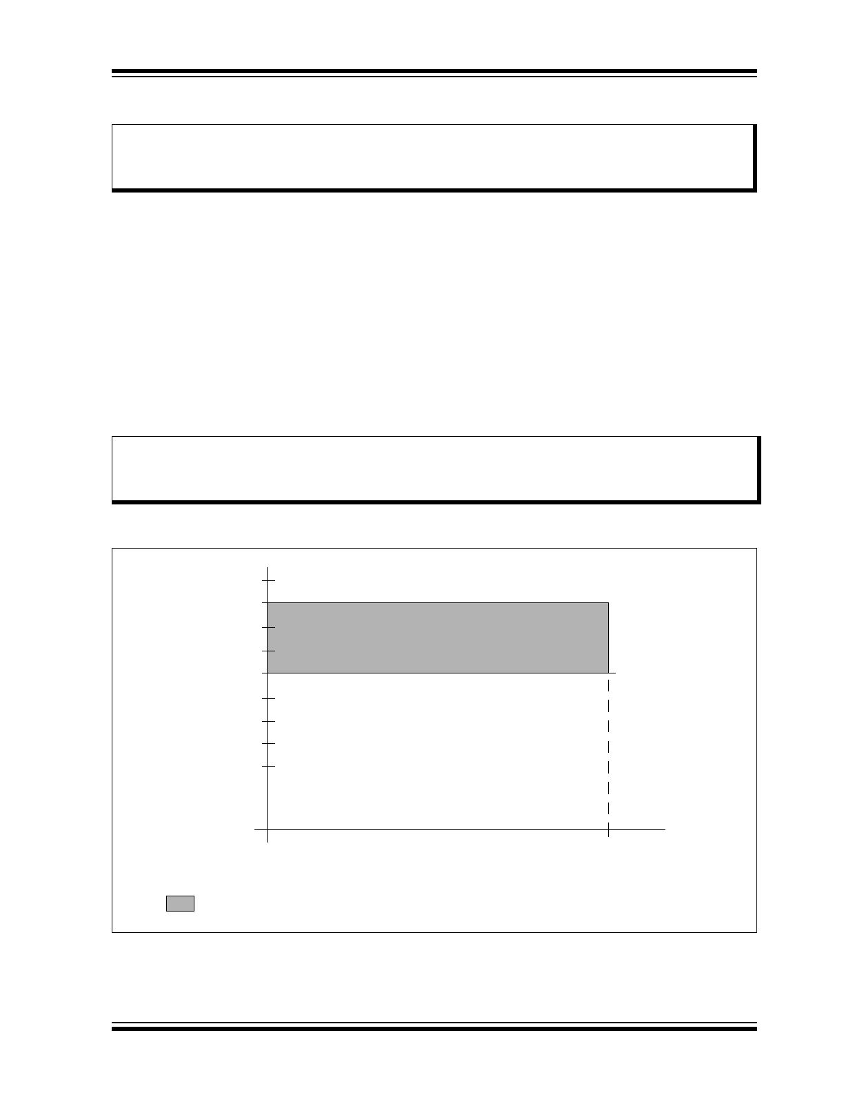
FIGURE 3-1:
PIC18F66K80 VOLTAGE-FREQUENCY GRAPH (HIGH TEMPERATURE)
Note:
Other than some basic data, this section documents only the high-temperature PIC18F66K80 family devices’
specifications that differ from those of the non-specialty PIC18F66K80 family devices. For detailed information
on the electrical specifications shared by the high-temperature and non-specialty devices, see the
“PIC18F66K80 Family Data Sheet”
(DS39977).
† NOTICE:
Stresses above those listed under “Absolute Maximum Ratings” may cause permanent damage to the
device. This is a stress rating only and functional operation of the device at those or any other conditions above
those indicated in the operation listings of this specification is not implied. Exposure to maximum rating conditions
for extended periods may affect device reliability.
Frequency
Vo
lt
a
g
e
6.0V
5.5V
4.0V
2.0V
64 MHz
3.5V
3.0V
2.5V
4.0V
4.5V
5.0V
High-Temperature Devices
PIC18F66K80 FAMILY
DS30509A-page 10
2012 Microchip Technology Inc.
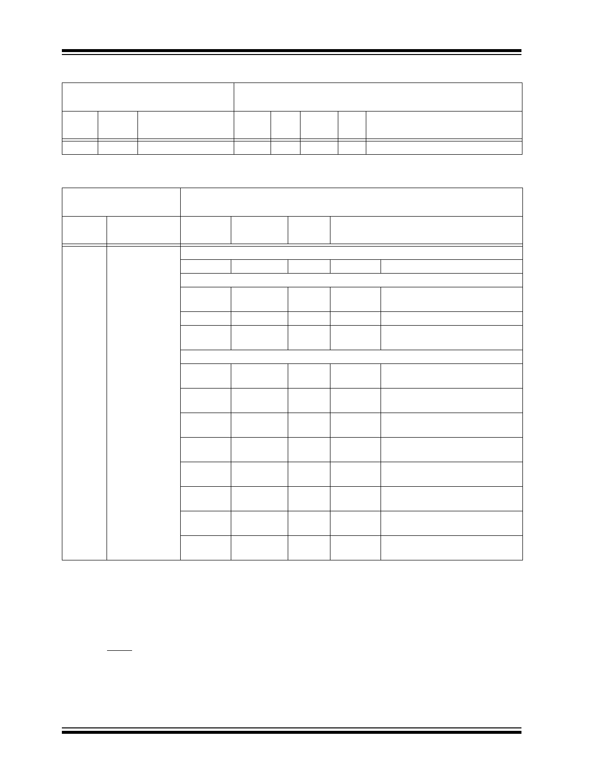
3.2
DC Characteristics: Supply Voltage (High Temperature)
PIC18F66K80 Family
(High Temperature)
Standard Operating Conditions (unless otherwise stated)
Operating temperature
+125°C
T
A
+150°C for high temperature
Param
No.
Symbol
Characteristic
Min
Typ
Max
Units
Conditions
D001
V
DD
Supply Voltage
4.0
—
5.5
V
For F devices
3.3
DC Characteristics: Power Down and Supply Current (High Temperature)
PIC18F66K80 Family
(High Temperature)
Standard Operating Conditions (unless otherwise stated)
Operating temperature
+125°C
T
A
+150°C for high temperature
Param
No.
Device
Typ
Max
Units
Conditions
PIC18FXXK80
Power-Down Current (I
PD
)
(
1
)
10
28
µA
+150°C
V
DD
= 5V, Sleep mode
Module Differential Currents
12
29
µA
+150°C
V
DD
= 5V,
Watchdog Timer Current: ΔI
WDT
12
28
µA
+150°C
V
DD
= 5V, A/D Current: ΔI
AD
12
28
µA
+150°C
V
DD
= 5V,
High/Low-Voltage Detect: ΔI
HLVD
Supply Current (I
DD
)
(
2
,
3
)
10
32
mA
+150°C
V
DD
= 5V, F
OSC
= 64 MHz
(PRI_RUN mode)
—
8
mA
+150°C
V
DD
= 5V, F
OSC
= 4 MHz
(PRI_RUN mode)
—
3
mA
+150°C
V
DD
= 5V, F
OSC
= 1 MHz
(PRI_RUN mode)
—
8
mA
+150°C
V
DD
= 5V, F
OSC
= 64 MHz
(PRI_IDLE mode)
—
1.8
mA
+150°C
V
DD
= 5V, F
OSC
= 4 MHz
(PRI_IDLE mode)
—
1
mA
+150°C
V
DD
= 5V, F
OSC
= 1 MHz
(PRI_IDLE mode)
—
28
mA
+150°C
V
DD
= 5V, F
OSC
= 64 MHz
(PRI_RUN mode, 16 MHz w/PLL)
—
8
mA
+150°C
V
DD
= 5V, F
OSC
= 16 MHz
(PRI_RUN mode, 4 MHz w/PLL)
Note 1:
The power-down current in Sleep mode does not depend on the oscillator type. Power-down current is
measured with the part in Sleep mode, with all I/O pins in a high-impedance state and tied to V
DD
or V
SS
,
and all features that add delta current are disabled (such as WDT, secondary oscillator, BOR, etc.).
2:
The supply current is mainly a function of operating voltage, frequency and mode. Other factors, such as
I/O pin loading and switching rate, oscillator type and circuit, internal code execution pattern and
temperature, also have an impact on the current consumption.
3:
The test conditions for all I
DD
measurements in active operation mode are:
OSC1 = External square wave, from rail-to-rail; all I/O pins tri-stated, pulled to V
DD
;
MCLR = V
DD
; WDT is enabled/disabled as specified.