
© 2009 Microchip Technology Inc.
DS39887C
PIC18F2458/2553/4458/4553
Data Sheet
28/40/44-Pin High-Performance,
Enhanced Flash, USB Microcontrollers
with 12-Bit A/D and nanoWatt Technology
DS39887C-page 2
© 2009 Microchip Technology Inc.
Information contained in this publication regarding device
applications and the like is provided only for your convenience
and may be superseded by updates. It is your responsibility to
ensure that your application meets with your specifications.
MICROCHIP MAKES NO REPRESENTATIONS OR
WARRANTIES OF ANY KIND WHETHER EXPRESS OR
IMPLIED, WRITTEN OR ORAL, STATUTORY OR
OTHERWISE, RELATED TO THE INFORMATION,
INCLUDING BUT NOT LIMITED TO ITS CONDITION,
QUALITY, PERFORMANCE, MERCHANTABILITY OR
FITNESS FOR PURPOSE. Microchip disclaims all liability
arising from this information and its use. Use of Microchip
devices in life support and/or safety applications is entirely at
the buyer’s risk, and the buyer agrees to defend, indemnify and
hold harmless Microchip from any and all damages, claims,
suits, or expenses resulting from such use. No licenses are
conveyed, implicitly or otherwise, under any Microchip
intellectual property rights.
Trademarks
The Microchip name and logo, the Microchip logo, dsPIC,
K
EE
L
OQ
, K
EE
L
OQ
logo, MPLAB, PIC, PICmicro, PICSTART,
rfPIC and UNI/O are registered trademarks of Microchip
Technology Incorporated in the U.S.A. and other countries.
FilterLab, Hampshire, HI-TECH C, Linear Active Thermistor,
MXDEV, MXLAB, SEEVAL and The Embedded Control
Solutions Company are registered trademarks of Microchip
Technology Incorporated in the U.S.A.
Analog-for-the-Digital Age, Application Maestro, CodeGuard,
dsPICDEM, dsPICDEM.net, dsPICworks, dsSPEAK, ECAN,
ECONOMONITOR, FanSense, HI-TIDE, In-Circuit Serial
Programming, ICSP, Mindi, MiWi, MPASM, MPLAB Certified
logo, MPLIB, MPLINK, mTouch, Octopus, Omniscient Code
Generation, PICC, PICC-18, PICDEM, PICDEM.net, PICkit,
PICtail, PIC
32
logo, REAL ICE, rfLAB, Select Mode, Total
Endurance, TSHARC, UniWinDriver, WiperLock and ZENA
are trademarks of Microchip Technology Incorporated in the
U.S.A. and other countries.
SQTP is a service mark of Microchip Technology Incorporated
in the U.S.A.
All other trademarks mentioned herein are property of their
respective companies.
© 2009, Microchip Technology Incorporated, Printed in the
U.S.A., All Rights Reserved.
Printed on recycled paper.
Note the following details of the code protection feature on Microchip devices:
•
Microchip products meet the specification contained in their particular Microchip Data Sheet.
•
Microchip believes that its family of products is one of the most secure families of its kind on the market today, when used in the
intended manner and under normal conditions.
•
There are dishonest and possibly illegal methods used to breach the code protection feature. All of these methods, to our
knowledge, require using the Microchip products in a manner outside the operating specifications contained in Microchip’s Data
Sheets. Most likely, the person doing so is engaged in theft of intellectual property.
•
Microchip is willing to work with the customer who is concerned about the integrity of their code.
•
Neither Microchip nor any other semiconductor manufacturer can guarantee the security of their code. Code protection does not
mean that we are guaranteeing the product as “unbreakable.”
Code protection is constantly evolving. We at Microchip are committed to continuously improving the code protection features of our
products. Attempts to break Microchip’s code protection feature may be a violation of the Digital Millennium Copyright Act. If such acts
allow unauthorized access to your software or other copyrighted work, you may have a right to sue for relief under that Act.
Microchip received ISO/TS-16949:2002 certification for its worldwide
headquarters, design and wafer fabrication facilities in Chandler and
Tempe, Arizona; Gresham, Oregon and design centers in California
and India. The Company’s quality system processes and procedures
are for its PIC
®
MCUs and dsPIC
®
DSCs, K
EE
L
OQ
®
code hopping
devices, Serial EEPROMs, microperipherals, nonvolatile memory and
analog products. In addition, Microchip’s quality system for the design
and manufacture of development systems is ISO 9001:2000 certified.
© 2009 Microchip Technology Inc.
DS39887C-page 3
PIC18F2458/2553/4458/4553
Universal Serial Bus Features:
• USB V2.0 Compliant
• Low Speed (1.5 Mb/s) and Full Speed (12 Mb/s)
• Supports Control, Interrupt, Isochronous and Bulk
Transfers
• Supports up to 32 Endpoints (16 bidirectional)
• 1-Kbyte Dual Access RAM for USB
• On-Chip USB Transceiver with On-Chip Voltage
Regulator
• Interface for Off-Chip USB Transceiver
• Streaming Parallel Port (SPP) for USB Streaming
Transfers (40/44-pin devices only)
Power-Managed Modes:
• Run: CPU On, Peripherals On
• Idle: CPU Off, Peripherals On
• Sleep: CPU Off, Peripherals Off
• Idle mode Currents Down to 5.8
μA Typical
• Sleep mode Currents Down to 0.1
μA Typical
• Timer1 Oscillator: 1.1
μA Typical, 32 kHz, 2V
• Watchdog Timer: 2.1
μA Typical
• Two-Speed Oscillator Start-up
Special Microcontroller Features:
• C Compiler Optimized Architecture with Optional
Extended Instruction Set
• 100,000 Erase/Write Cycle Enhanced Flash
Program Memory Typical
• 1,000,000 Erase/Write Cycle Data EEPROM
Memory Typical
• Flash/Data EEPROM Retention: > 40 Years
• Self-Programmable under Software Control
• Priority Levels for Interrupts
• 8 x 8 Single-Cycle Hardware Multiplier
• Extended Watchdog Timer (WDT):
- Programmable period from 41 ms to 131s
• Programmable Code Protection
• Single-Supply 5V In-Circuit Serial
Programming™ (ICSP™) via Two Pins
• In-Circuit Debug (ICD) via Two Pins
• Optional Dedicated ICD/ICSP Port (44-pin TQFP
package only)
• Wide Operating Voltage Range (2.0V to 5.5V)
Flexible Oscillator Structure:
• Four Crystal modes, Including High-Precision PLL
for USB
• Two External Clock modes, up to 48 MHz
• Internal Oscillator Block:
- 8 user-selectable frequencies, from 31 kHz
to 8 MHz
- User-tunable to compensate for frequency drift
• Secondary Oscillator using Timer1 @ 32 kHz
• Dual Oscillator Options allow Microcontroller and
USB module to Run at Different Clock Speeds
• Fail-Safe Clock Monitor:
- Allows for safe shutdown if any clock stops
Peripheral Highlights:
• High-Current Sink/Source: 25 mA/25 mA
• Three External Interrupts
• Four Timer modules (Timer0 to Timer3)
• Up to 2 Capture/Compare/PWM (CCP) modules:
- Capture is 16-bit, max. resolution 5.2 ns (T
CY
/16)
- Compare is 16-bit, max. resolution 83.3 ns (T
CY
)
- PWM output: PWM resolution is 1 to 10-bits
• Enhanced Capture/Compare/PWM (ECCP) module:
- Multiple output modes
- Selectable polarity
- Programmable dead time
- Auto-shutdown and auto-restart
• Enhanced USART module:
- LIN bus support
• Master Synchronous Serial Port (MSSP) module
supporting 3-wire SPI (all 4 modes) and I
2
C™
Master and Slave modes
• 12-Bit, up to 13-Channel Analog-to-Digital Converter
module (A/D) with Programmable Acquisition Time
• Dual Analog Comparators with Input Multiplexing
Note:
This document is supplemented by
the “PIC18F2455/2550/4455/4550 Data
Sheet” (DS39632). See Section 1.0
“Device Overview”.
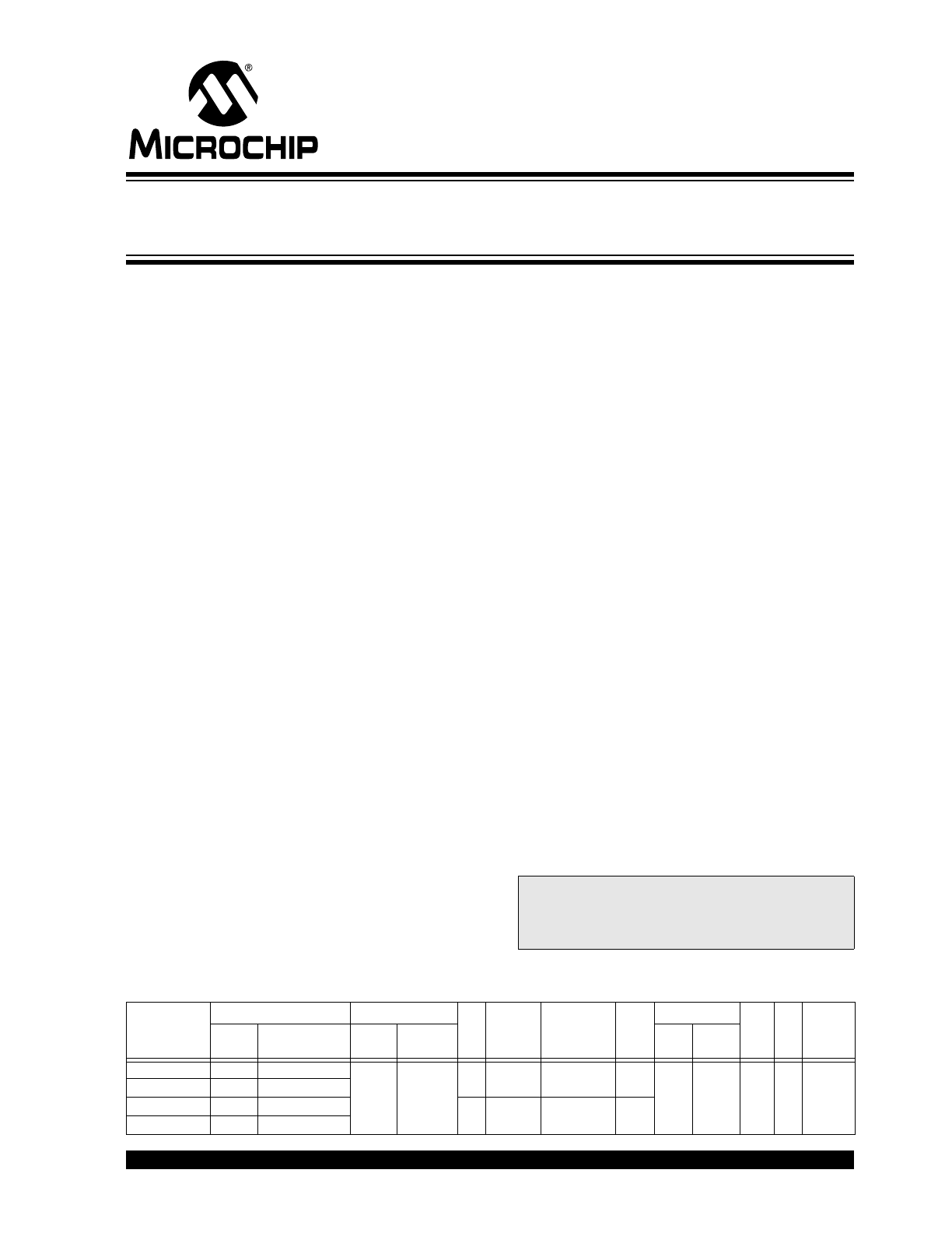
Device
Program Memory
Data Memory
I/O
12-Bit
A/D (ch)
CCP/ECCP
(PWM)
SPP
MSSP
EU
SA
R
T
Co
m
p
.
Timers
8/16-Bit
Flash
(bytes)
# Single-Word
Instructions
SRAM
(bytes)
EEPROM
(bytes)
SPI
Master
I
2
C™
PIC18F2458
24K
12288
2048
256
24
10
2/0
No
Y
Y
1
2
1/3
PIC18F2553
32K
16384
PIC18F4458
24K
12288
35
13
1/1
Yes
PIC18F4553
32K
16384
28/40/44-Pin High-Performance, Enhanced Flash, USB
Microcontrollers with 12-Bit A/D and nanoWatt Technology
PIC18F2458/2553/4458/4553
DS39887C-page 4
© 2009 Microchip Technology Inc.
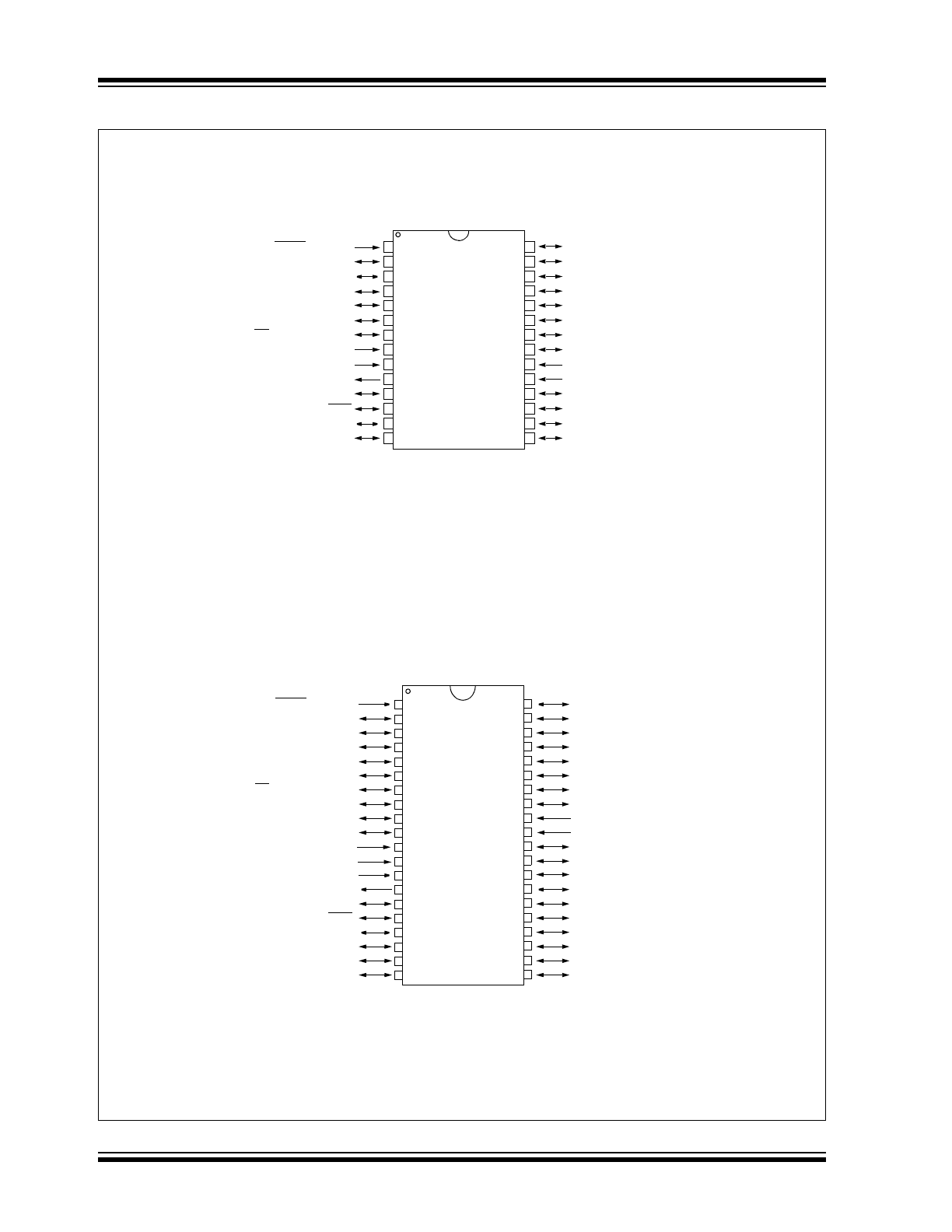
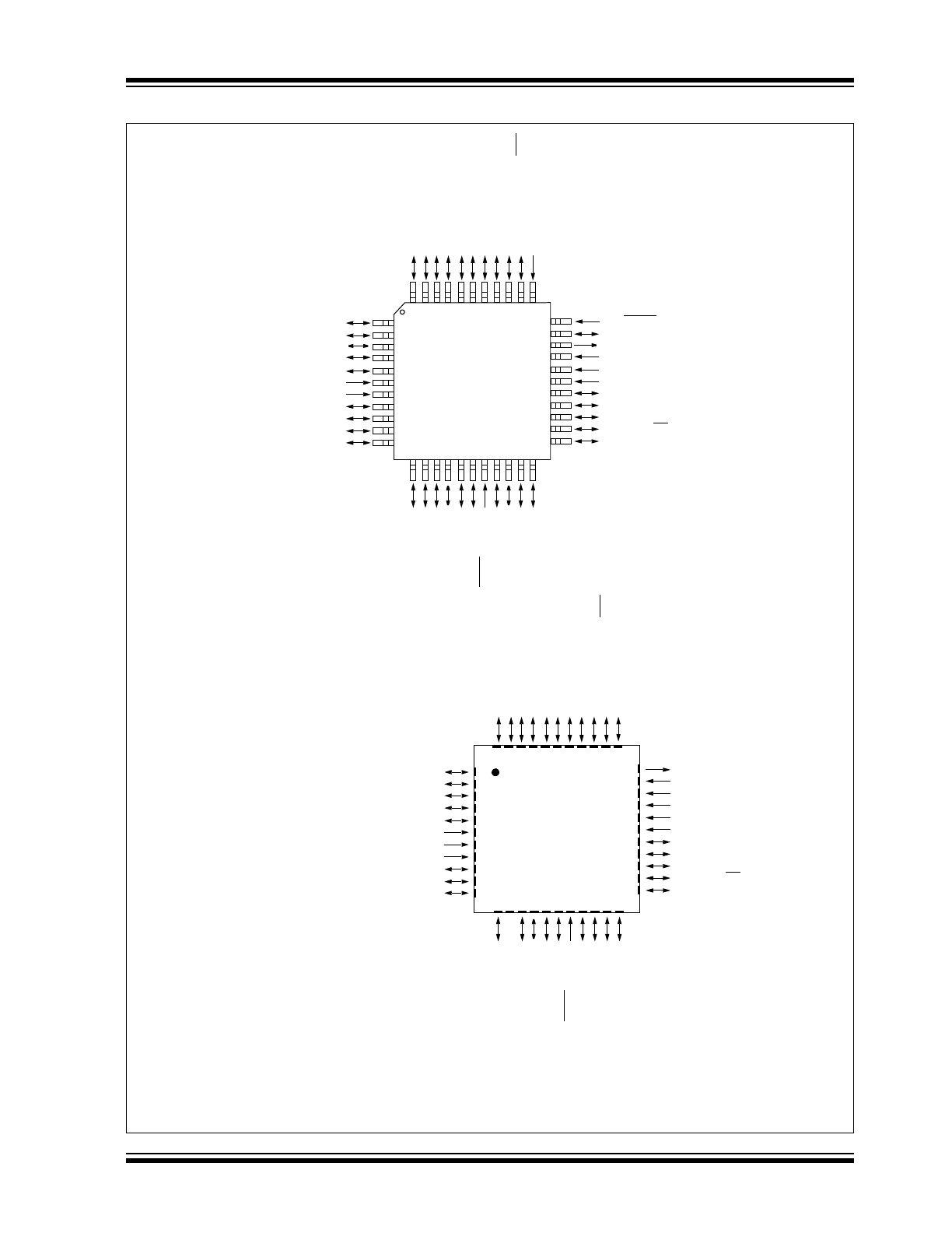
Pin Diagrams
40-Pin PDIP
PIC18
F
24
58
28-Pin SPDIP, SOIC
PI
C
18F
255
3
10
11
2
3
4
5
6
1
8
7
9
12
13
14
15
16
17
18
19
20
23
24
25
26
27
28
22
21
MCLR/V
PP
/RE3
RA0/AN0
RA1/AN1
RA2/AN2/V
REF
-/CV
REF
RA3/AN3/V
REF
+
RA4/T0CKI/C1OUT/RCV
RA5/AN4/SS/HLVDIN/C2OUT
V
SS
OSC1/CLKI
OSC2/CLKO/RA6
RC0/T1OSO/T13CKI
RC1/T1OSI/CCP2
(1)
/UOE
RC2/CCP1
V
USB
RB7/KBI3/PGD
RB6/KBI2/PGC
RB5/KBI1/PGM
RB4/AN11/KBI0
RB3/AN9/CCP2
(1)
/VPO
RB2/AN8/INT2/VMO
RB1/AN10/INT1/SCK/SCL
RB0/AN12/INT0/FLT0/SDI/SDA
V
DD
V
SS
RC7/RX/DT/SDO
RC6/TX/CK
RC5/D+/VP
RC4/D-/VM
RB7/KBI3/PGD
RB6/KBI2/PGC
RB5/KBI1/PGM
RB4/AN11/KBI0/CSSPP
RB3/AN9/CCP2
(1)
/VPO
RB2/AN8/INT2/VMO
RB1/AN10/INT1/SCK/SCL
RB0/AN12/INT0/FLT0/SDI/SDA
V
DD
V
SS
RD7/SPP7/P1D
RD6/SPP6/P1C
RD5/SPP5/P1B
RD4/SPP4
RC7/RX/DT/SDO
RC6/TX/CK
RC5/D+/VP
RC4/D-/VM
RD3/SPP3
RD2/SPP2
MCLR/V
PP
/RE3
RA0/AN0
RA1/AN1
RA2/AN2/V
REF
-/CV
REF
RA3/AN3/V
REF
+
RA4/T0CKI/C1OUT/RCV
RA5/AN4/SS/HLVDIN/C2OUT
RE0/AN5/CK1SPP
RE1/AN6/CK2SPP
RE2/AN7/OESPP
V
DD
V
SS
OSC1/CLKI
OSC2/CLKO/RA6
RC0/T1OSO/T13CKI
RC1/T1OSI/CCP2
(1)
/UOE
RC2/CCP1/P1A
V
USB
RD0/SPP0
RD1/SPP1
1
2
3
4
5
6
7
8
9
10
11
12
13
14
15
16
17
18
19
20
40
39
38
37
36
35
34
33
32
31
30
29
28
27
26
25
24
23
22
21
PIC
1
8F
44
58
PIC
1
8F
45
53
Note 1:
RB3 is the alternate pin for CCP2 multiplexing.
© 2009 Microchip Technology Inc.
DS39887C-page 5
PIC18F2458/2553/4458/4553
Pin Diagrams (Continued)
44-Pin TQFP
44-Pin QFN
PIC18F4458
PIC18F4458
10
11
2
3
6
1
18 19
20 21 22
12
13 14 15
38
8
7
44
43 42 41
40 39
16 17
29
30
31
32
33
23
24
25
26
27
28
36
34
35
9
37
RA3
/AN3
/V
RE
F
+
RA2
/A
N
2/
V
RE
F
-/C
V
RE
F
RA1
/AN1
RA0
/AN0
MC
LR
/V
PP
/RE
3
NC/
ICCK
(2
)
/ICP
G
C
(2
)
RB7
/KBI
3
/PG
D
RB6
/KBI
2
/PG
C
RB
5
/KBI
1/
PG
M
RB4
/AN1
1/
K
B
I0
/C
SSP
P
NC/ICDT
(2
)
/ICP
G
D
(2
)
RC6
/T
X
/CK
RC5
/D+/VP
RC4
/D-
/V
M
RD3
/SPP
3
RD2
/SPP
2
RD1
/SPP
1
RD0
/SPP
0
V
US
B
RC2
/CCP1
/P1
A
RC
1/
T
1OS
I/C
C
P
2
(1
)
/U
OE
NC/
ICPOR
T
S
(2
)
NC/ICRST
(2)
/ICV
PP(2)
RC0/T1OSO/T13CKI
OSC2/CLKO/RA6
OSC1/CLKI
V
SS
V
DD
RE2/AN7/OESPP
RE1/AN6/CK2SPP
RE0/AN5/CK1SPP
RA5/AN4/SS/HLVDIN/C2OUT
RA4/T0CKI/C1OUT/RCV
RC7/RX/DT/SDO
RD4/SPP4
RD5/SPP5/P1B
RD6/SPP6/P1C
V
SS
V
DD
RB0/AN12/INT0/FLT0/SDI/SDA
RB1/AN10/INT1/SCK/SCL
RB2/AN8/INT2/VMO
RB3/AN9/CCP2
(1)
/VPO
RD7/SPP7/P1D
5
4
10
11
2
3
6
1
18
19
20 21
22
12 13
14 15
38
8
7
44
43
42 41
40 39
16 17
29
30
31
32
33
23
24
25
26
27
28
36
34
35
9
37
RA
3
/AN3
/V
RE
F
+
R
A
2/A
N
2/V
RE
F
-/C
V
RE
F
RA1
/AN1
RA0
/AN0
MC
L
R
/V
PP
/RE
3
RB
7
/K
B
I3
/P
GD
RB
6
/K
B
I2
/P
GC
RB5
/KBI
1/
PG
M
RB4
/AN1
1/
KBI
0/
CSSPP
NC
RC6
/T
X/CK
RC5
/D
+/VP
RC4
/D
-/
VM
RD3
/SPP3
RD2
/SPP2
RD1
/SPP1
RD0
/SPP0
V
US
B
RC2
/C
CP
1
/P1
A
RC1
/T
1O
S
I/C
CP2
(1
)
/U
OE
RC0
/T
1
O
SO/T
13
CK
I
OSC2/CLKO/RA6
OSC1/CLKI
V
SS
V
DD
RE2/AN7/OESPP
RE1/AN6/CK2SPP
RE0/AN5/CK1SPP
RA5/AN4/SS/HLVDIN/C2OUT
RA4/T0CKI/C1OUT/RCV
RC7/RX/DT/SDO
RD4/SPP4
RD5/SPP5/P1B
RD6/SPP6/P1C
V
SS
V
DD
RB0/AN12/INT0/FLT0/SDI/SDA
RB1/AN10/INT1/SCK/SCL
RB2/AN8/INT2/VMO
R
B
3/
AN9
/CC
P2
(1
)
/VPO
RD7/SPP7/P1D
5
4
V
SS
V
DD
V
DD
Note
1:
RB3 is the alternate pin for CCP2 multiplexing.
2:
Special ICPORT features are available only in 44-pin TQFP packages. See Section 25.9 “Special ICPORT Features” in
the “PIC18F2455/2550/4455/4550 Data Sheet”’.
PIC18F4553
PIC18F4553

PIC18F2458/2553/4458/4553
DS39887C-page 6
© 2009 Microchip Technology Inc.
Table of Contents
1.0
Device Overview .......................................................................................................................................................................... 7
2.0
12-Bit Analog-to-Digital Converter (A/D) Module ....................................................................................................................... 21
3.0
Special Features of the CPU...................................................................................................................................................... 31
4.0
Electrical Characteristics ............................................................................................................................................................ 33
5.0
Packaging Information................................................................................................................................................................ 37
Appendix A: Revision History............................................................................................................................................................... 39
Appendix B: Device Differences........................................................................................................................................................... 39
Appendix C: Migration From Mid-Range to Enhanced Devices........................................................................................................... 40
Appendix D: Migration From High-End to Enhanced Devices ............................................................................................................. 40
Index .................................................................................................................................................................................................... 41
The Microchip Web Site ....................................................................................................................................................................... 43
Customer Change Notification Service ................................................................................................................................................ 43
Customer Support ................................................................................................................................................................................ 43
Reader Response ................................................................................................................................................................................ 44
Product Identification System............................................................................................................................................................... 45
TO OUR VALUED CUSTOMERS
It is our intention to provide our valued customers with the best documentation possible to ensure successful use of your Microchip
products. To this end, we will continue to improve our publications to better suit your needs. Our publications will be refined and
enhanced as new volumes and updates are introduced.
If you have any questions or comments regarding this publication, please contact the Marketing Communications Department via
E-mail at docerrors@microchip.com or fax the Reader Response Form in the back of this data sheet to (480) 792-4150. We
welcome your feedback.
Most Current Data Sheet
To obtain the most up-to-date version of this data sheet, please register at our Worldwide Web site at:
http://www.microchip.com
You can determine the version of a data sheet by examining its literature number found on the bottom outside corner of any page.
The last character of the literature number is the version number, (e.g., DS30000A is version A of document DS30000).
Errata
An errata sheet, describing minor operational differences from the data sheet and recommended workarounds, may exist for current
devices. As device/documentation issues become known to us, we will publish an errata sheet. The errata will specify the revision
of silicon and revision of document to which it applies.
To determine if an errata sheet exists for a particular device, please check with one of the following:
• Microchip’s Worldwide Web site; http://www.microchip.com
• Your local Microchip sales office (see last page)
When contacting a sales office, please specify which device, revision of silicon and data sheet (include literature number) you are
using.
Customer Notification System
Register on our web site at www.microchip.com to receive the most current information on all of our products.

© 2009 Microchip Technology Inc.
DS39887C-page 7
PIC18F2458/2553/4458/4553
1.0
DEVICE OVERVIEW
This document contains device-specific information for
the following devices:
The PIC18F4553 family of devices offers the advan-
tages of all PIC18 microcontrollers – namely, high
computational performance at an economical price –
with the addition of high-endurance, Enhanced Flash
program memory. In addition to these features, the
PIC18F4553 family introduces design enhancements
that make these microcontrollers a logical choice for
many high-performance, power sensitive applications.
1.1
Special Features
• 12-Bit A/D Converter: The PIC18F4553 family
implements a 12-bit A/D Converter. The A/D
Converter incorporates programmable acquisi-
tion time. This allows for a channel to be selected
and a conversion to be initiated, without waiting
for a sampling period and thus, reducing code
overhead.
1.2
Details on Individual Family
Members
The PIC18F2458/2553/4458/4553 devices are
available in 28-pin and 40/44-pin packages. Block
diagrams for the two groups are shown in Figure 1-1
and Figure 1-2.
The devices are differentiated from each other in the
following ways:
1.
Flash program memory (24 Kbytes for
PIC18FX458 devices, 32 Kbytes for
PIC18FX553).
2.
A/D channels (10 for 28-pin devices, 13 for
40-pin and 44-pin devices).
3.
I/O ports (3 bidirectional ports and 1 input only
port on 28-pin devices, 5 bidirectional ports on
40-pin and 44-pin devices).
4.
CCP and Enhanced CCP implementation
(28-pin devices have two standard CCP
modules, 40-pin and 44-pin devices have one
standard CCP module and one ECCP module).
5.
Streaming Parallel Port (present only on
40/44-pin devices).
All other features for devices in this family are identical.
These are summarized in Table 1-1.
The pinouts for all devices are listed in Table 1-2 and
Table 1-3.
Members of the PIC18F4553 family are available as
both standard and low-voltage devices. Standard
devices with Enhanced Flash memory, designated with
an “F” in the part number (such as PIC18F2458),
accommodate an operating V
DD
range of 4.2V to 5.5V.
Low-voltage parts, designated by “LF” (such as
PIC18LF2458), function over an extended V
DD
range
of 2.0V to 5.5V.
• PIC18F2458
• PIC18F4458
• PIC18F2553
• PIC18F4553
Note:
This data sheet documents only the
devices’ features and specifications that are
in addition to the features and specifica-
tions of the PIC18F2455/2550/4455/4550
devices. For information on the features
and specifications shared by
the PIC18F2458/2553/4458/4553 and
PIC18F2455/2550/4455/4550 devices,
see
the
“
PIC18F2455/2550/4455/4550
Data Sheet” (DS39632).
PIC18F2458/2553/4458/4553
DS39887C-page 8
© 2009 Microchip Technology Inc.
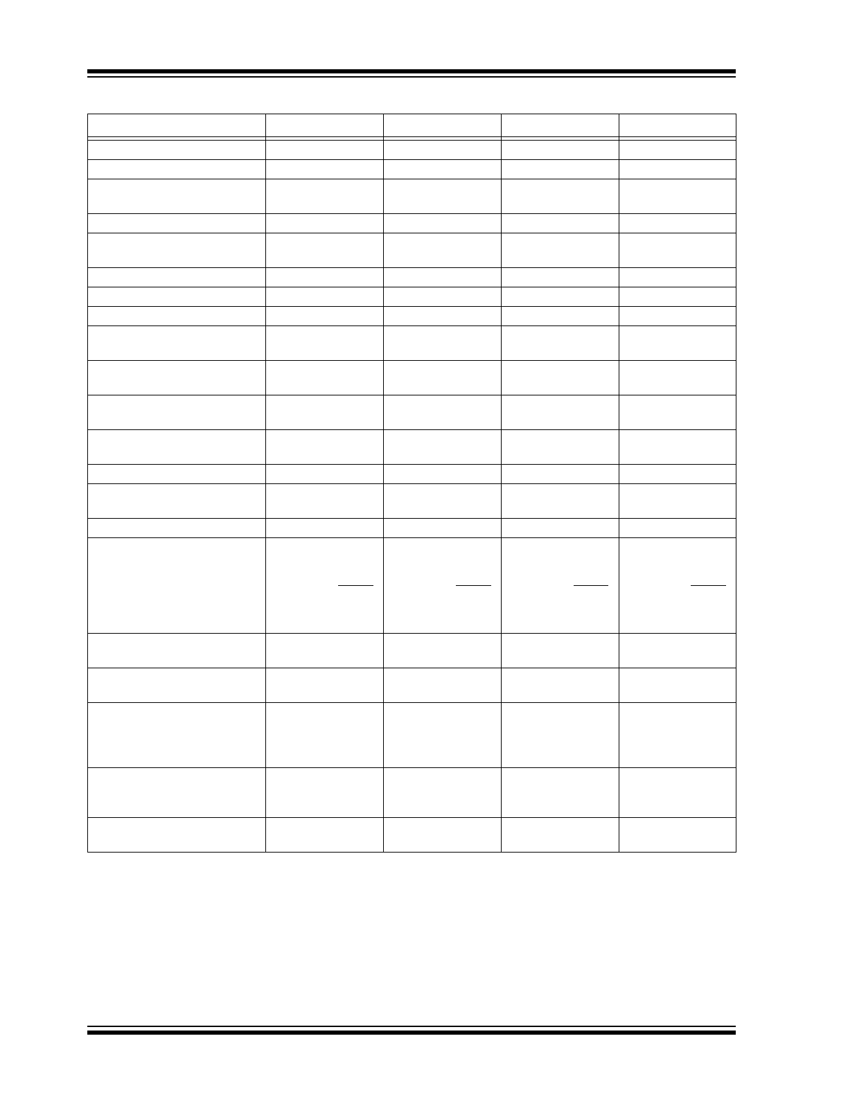
TABLE 1-1:
DEVICE FEATURES
Features
PIC18F2458 PIC18F2553 PIC18F4458 PIC18F4553
Operating Frequency
DC – 48 MHz
DC – 48 MHz
DC – 48 MHz
DC – 48 MHz
Program Memory (Bytes)
24576
32768
24576
32768
Program Memory
(Instructions)
12288 16384 12288 16384
Data
Memory
(Bytes) 2048 2048 2048 2048
Data EEPROM Memory
(Bytes)
256 256 256 256
Interrupt
Sources
19 19 20 20
I/O Ports
Ports A, B, C, (E)
Ports A, B, C, (E)
Ports A, B, C, D, E
Ports A, B, C, D, E
Timers
4 4 4 4
Capture/Compare/PWM
Modules
2 2 1 1
Enhanced Capture/
Compare/PWM Modules
0 0 1 1
Serial Communications
MSSP,
Enhanced USART
MSSP,
Enhanced USART
MSSP,
Enhanced USART
MSSP,
Enhanced USART
Universal Serial Bus (USB)
Module
1 1 1 1
Streaming Parallel Port (SPP)
No
No
Yes
Yes
12-Bit Analog-to-Digital
Converter Module
10 Input Channels 10 Input Channels 13 Input Channels 13 Input Channels
Comparators
2 2 2 2
Resets (and Delays)
POR, BOR, WDT,
RESET Instruction,
Stack Full, Stack
Underflow, MCLR
(optional),
(PWRT, OST)
POR, BOR, WDT,
RESET Instruction,
Stack Full, Stack
Underflow, MCLR
(optional),
(PWRT, OST)
POR, BOR, WDT,
RESET Instruction,
Stack Full, Stack
Underflow, MCLR
(optional),
(PWRT, OST)
POR, BOR, WDT,
RESET Instruction,
Stack Full, Stack
Underflow, MCLR
(optional),
(PWRT, OST)
Programmable High/
Low-Voltage Detect
Yes
Yes
Yes
Yes
Programmable Brown-out
Reset
Yes Yes Yes Yes
Instruction Set
75 Instructions;
83 with Extended
Instruction Set
Enabled
75 Instructions;
83 with Extended
Instruction Set
Enabled
75 Instructions;
83 with Extended
Instruction Set
Enabled
75 Instructions;
83 with Extended
Instruction Set
Enabled
Packages
28-Pin SPDIP
28-Pin SOIC
28-Pin SPDIP
28-Pin SOIC
40-Pin PDIP
44-Pin QFN
44-Pin TQFP
40-Pin PDIP
44-Pin QFN
44-Pin TQFP
Corresponding Devices with
10-Bit A/D
PIC18F2455
PIC18F2550
PIC18F4455
PIC18F4550
© 2009 Microchip Technology Inc.
DS39887C-page 9
PIC18F2458/2553/4458/4553
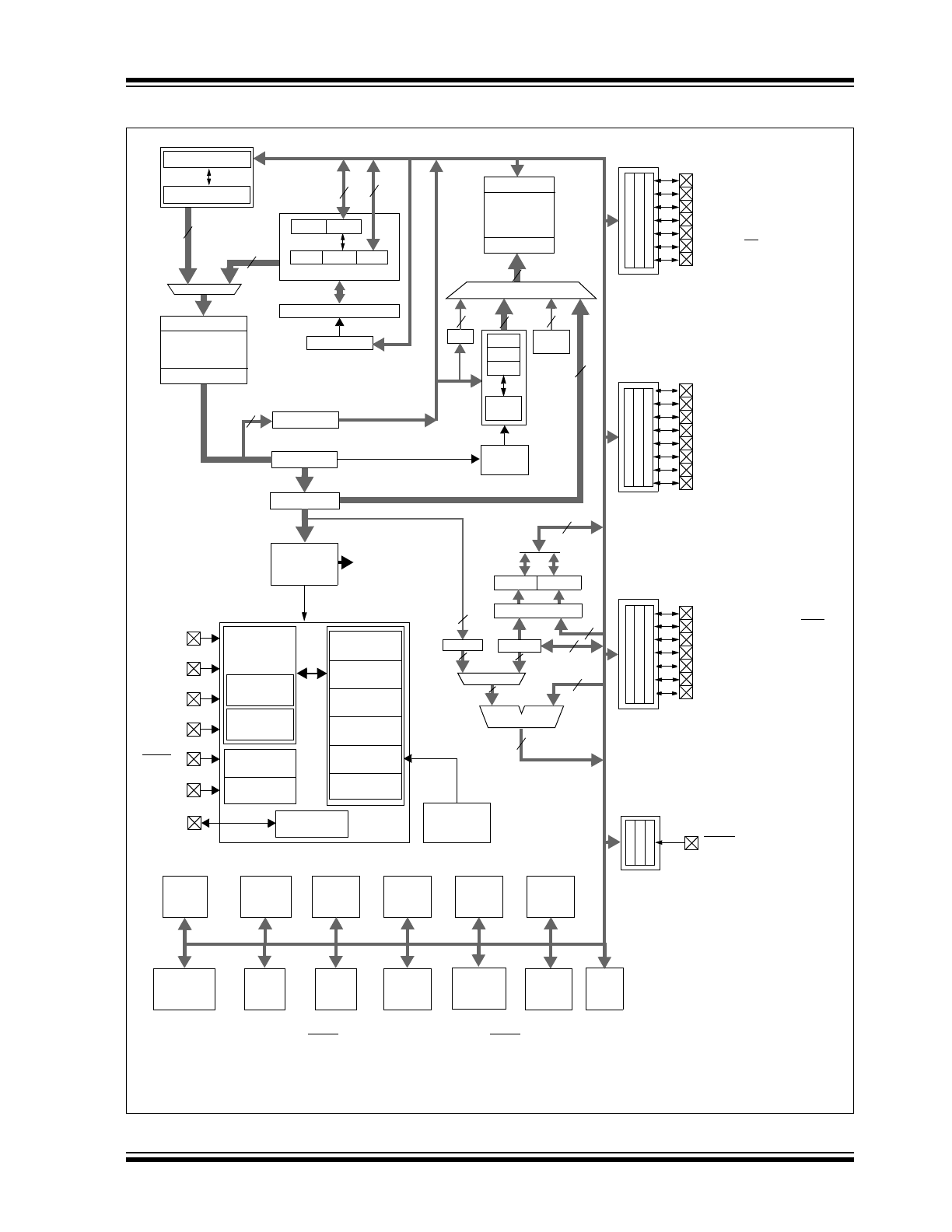
FIGURE 1-1:
PIC18F2458/2553 (28-PIN) BLOCK DIAGRAM
Data Latch
Data Memory
(2 Kbytes)
Address Latch
Data Address<12>
12
Access
BSR
4
4
PCH PCL
PCLATH
8
31 Level Stack
Program Counter
PRODL
PRODH
8 x 8 Multiply
8
8
8
ALU<8>
Address Latch
Program Memory
(24/32 Kbytes)
Data Latch
20
8
8
Table Pointer<21>
inc/dec logic
21
8
Data Bus<8>
Table Latch
8
IR
12
3
ROM Latch
PCLATU
PCU
PORTE
MCLR/V
PP
/RE3
(1)
Note 1:
RE3 is multiplexed with MCLR and is only available when the MCLR Resets are disabled.
2:
OSC1/CLKI and OSC2/CLKO are only available in select oscillator modes and when these pins are not being used as digital I/O.
3:
RB3 is the alternate pin for CCP2 multiplexing.
W
Instruction Bus <16>
STKPTR
Bank
8
8
8
BITOP
FSR0
FSR1
FSR2
inc/dec
Address
12
Decode
logic
EUSART
Comparator
MSSP
12-Bit
ADC
Timer2
Timer1
Timer3
Timer0
HLVD
CCP2
BOR
Data
EEPROM
USB
Instruction
Decode &
Control
State Machine
Control Signals
Power-up
Timer
Oscillator
Start-up Timer
Power-on
Reset
Watchdog
Timer
OSC1
(2)
OSC2
(2)
V
DD
,
Brown-out
Reset
Internal
Oscillator
Fail-Safe
Clock Monitor
Reference
Band Gap
V
SS
MCLR
(1)
Block
INTRC
Oscillator
8 MHz
Oscillator
Single-Supply
Programming
In-Circuit
Debugger
T1OSI
T1OSO
USB Voltage
Regulator
V
USB
PORTB
PORTC
RB0/AN12/INT0/FLT0/SDI/SDA
RC0/T1OSO/T13CKI
RC1/T1OSI/CCP2
(3)
/UOE
RC2/CCP1
RC4/D-/VM
RC5/D+/VP
RC6/TX/CK
RC7/RX/DT/SDO
RB1/AN10/INT1/SCK/SCL
RB2/AN8/INT2/VMO
RB3/AN9/CCP2
(3)
/VPO
RB4/AN11/KBI0
RB5/KBI1/PGM
RB6/KBI2/PGC
RB7/KBI3/PGD
PORTA
RA4/T0CKI/C1OUT/RCV
RA5/AN4/SS/HLVDIN/C2OUT
RA3/AN3/V
REF
+
RA2/AN2/V
REF
-/CV
REF
RA1/AN1
RA0/AN0
OSC2/CLKO/RA6
CCP1
PIC18F2458/2553/4458/4553
DS39887C-page 10
© 2009 Microchip Technology Inc.
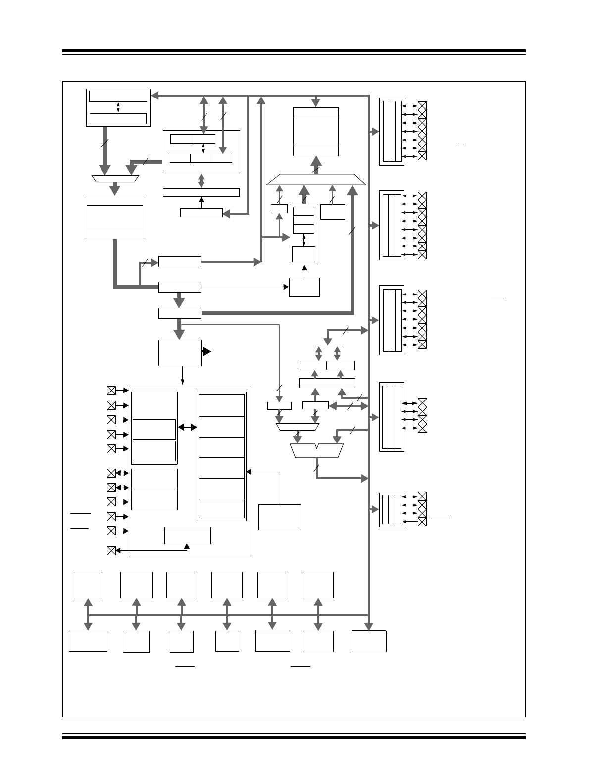
FIGURE 1-2:
PIC18F4458/4553(40/44-PIN) BLOCK DIAGRAM
Instruction
Decode &
Control
Data Latch
Data Memory
(2 Kbytes)
Address Latch
Data Address<12>
12
Access
BSR
4
4
PCH PCL
PCLATH
8
31 Level Stack
Program Counter
PRODL
PRODH
8 x 8 Multiply
8
BITOP
8
8
ALU<8>
Address Latch
Program Memory
(24/32 Kbytes)
Data Latch
20
8
8
Table Pointer<21>
inc/dec logic
21
8
Data Bus<8>
Table Latch
8
IR
12
3
ROM Latch
PORTD
RD0/SPP0:RD4/SPP4
PCLATU
PCU
PORTE
MCLR/V
PP
/RE3
(1)
RE2/AN7/OESPP
RE0/AN5/CK1SPP
RE1/AN6/CK2SPP
Note 1:
RE3 is multiplexed with MCLR and is only available when the MCLR Resets are disabled.
2:
OSC1/CLKI and OSC2/CLKO are only available in select oscillator modes and when these pins are not being used as digital I/O.
3:
These pins are only available on 44-pin TQFP packages under certain conditions.
4:
RB3 is the alternate pin for CCP2 multiplexing.
EUSART
Comparator
MSSP
12-Bit
ADC
Timer2
Timer1
Timer3
Timer0
CCP2
HLVD
ECCP1
BOR
Data
EEPROM
W
Instruction Bus <16>
STKPTR
Bank
8
State Machine
Control Signals
8
8
Power-up
Timer
Oscillator
Start-up Timer
Power-on
Reset
Watchdog
Timer
OSC1
(2)
OSC2
(2)
V
DD
, V
SS
Brown-out
Reset
Internal
Oscillator
Fail-Safe
Clock Monitor
Reference
Band Gap
MCLR
(1)
Block
INTRC
Oscillator
8 MHz
Oscillator
Single-Supply
Programming
In-Circuit
Debugger
T1OSI
T1OSO
RD5/SPP5/P1B
RD6/SPP6/P1C
RD7/SPP7/P1D
PORTA
PORTB
PORTC
RA4/T0CKI/C1OUT/RCV
RA5/AN4/SS/HLVDIN/C2OUT
RB0/AN12/INT0/FLT0/SDI/SDA
RC0/T1OSO/T13CKI
RC1/T1OSI/CCP2
(4)
/UOE
RC2/CCP1/P1A
RC4/D-/VM
RC5/D+/VP
RC6/TX/CK
RC7/RX/DT/SDO
RA3/AN3/V
REF
+
RA2/AN2/V
REF
-/CV
REF
RA1/AN1
RA0/AN0
RB1/AN10/INT1/SCK/SCL
RB2/AN8/INT2/VMO
RB3/AN9/CCP2
(4)
/VPO
OSC2/CLKO/RA6
RB4/AN11/KBI0/CSSPP
RB5/KBI1/PGM
RB6/KBI2/PGC
RB7/KBI3/PGD
USB
FSR0
FSR1
FSR2
inc/dec
Address
12
Decode
logic
USB Voltage
Regulator
V
USB
ICRST
(3)
ICPGC
(3)
ICPGD
(3)
ICPORTS
(3)