
© 2009 Microchip Technology Inc.
DS39755C
PIC18F2423/2523/4423/4523
Data Sheet
28/40/44-Pin, Enhanced Flash
Microcontrollers with 12-Bit A/D
and nanoWatt Technology
DS39755C-page 2
© 2009 Microchip Technology Inc.
Information contained in this publication regarding device
applications and the like is provided only for your convenience
and may be superseded by updates. It is your responsibility to
ensure that your application meets with your specifications.
MICROCHIP MAKES NO REPRESENTATIONS OR
WARRANTIES OF ANY KIND WHETHER EXPRESS OR
IMPLIED, WRITTEN OR ORAL, STATUTORY OR
OTHERWISE, RELATED TO THE INFORMATION,
INCLUDING BUT NOT LIMITED TO ITS CONDITION,
QUALITY, PERFORMANCE, MERCHANTABILITY OR
FITNESS FOR PURPOSE. Microchip disclaims all liability
arising from this information and its use. Use of Microchip
devices in life support and/or safety applications is entirely at
the buyer’s risk, and the buyer agrees to defend, indemnify and
hold harmless Microchip from any and all damages, claims,
suits, or expenses resulting from such use. No licenses are
conveyed, implicitly or otherwise, under any Microchip
intellectual property rights.
Trademarks
The Microchip name and logo, the Microchip logo, dsPIC,
K
EE
L
OQ
, K
EE
L
OQ
logo, MPLAB, PIC, PICmicro, PICSTART,
rfPIC and UNI/O are registered trademarks of Microchip
Technology Incorporated in the U.S.A. and other countries.
FilterLab, Hampshire, HI-TECH C, Linear Active Thermistor,
MXDEV, MXLAB, SEEVAL and The Embedded Control
Solutions Company are registered trademarks of Microchip
Technology Incorporated in the U.S.A.
Analog-for-the-Digital Age, Application Maestro, CodeGuard,
dsPICDEM, dsPICDEM.net, dsPICworks, dsSPEAK, ECAN,
ECONOMONITOR, FanSense, HI-TIDE, In-Circuit Serial
Programming, ICSP, Mindi, MiWi, MPASM, MPLAB Certified
logo, MPLIB, MPLINK, mTouch, Octopus, Omniscient Code
Generation, PICC, PICC-18, PICDEM, PICDEM.net, PICkit,
PICtail, PIC
32
logo, REAL ICE, rfLAB, Select Mode, Total
Endurance, TSHARC, UniWinDriver, WiperLock and ZENA
are trademarks of Microchip Technology Incorporated in the
U.S.A. and other countries.
SQTP is a service mark of Microchip Technology Incorporated
in the U.S.A.
All other trademarks mentioned herein are property of their
respective companies.
© 2009, Microchip Technology Incorporated, Printed in the
U.S.A., All Rights Reserved.
Printed on recycled paper.
Note the following details of the code protection feature on Microchip devices:
•
Microchip products meet the specification contained in their particular Microchip Data Sheet.
•
Microchip believes that its family of products is one of the most secure families of its kind on the market today, when used in the
intended manner and under normal conditions.
•
There are dishonest and possibly illegal methods used to breach the code protection feature. All of these methods, to our
knowledge, require using the Microchip products in a manner outside the operating specifications contained in Microchip’s Data
Sheets. Most likely, the person doing so is engaged in theft of intellectual property.
•
Microchip is willing to work with the customer who is concerned about the integrity of their code.
•
Neither Microchip nor any other semiconductor manufacturer can guarantee the security of their code. Code protection does not
mean that we are guaranteeing the product as “unbreakable.”
Code protection is constantly evolving. We at Microchip are committed to continuously improving the code protection features of our
products. Attempts to break Microchip’s code protection feature may be a violation of the Digital Millennium Copyright Act. If such acts
allow unauthorized access to your software or other copyrighted work, you may have a right to sue for relief under that Act.
Microchip received ISO/TS-16949:2002 certification for its worldwide
headquarters, design and wafer fabrication facilities in Chandler and
Tempe, Arizona; Gresham, Oregon and design centers in California
and India. The Company’s quality system processes and procedures
are for its PIC
®
MCUs and dsPIC
®
DSCs, K
EE
L
OQ
®
code hopping
devices, Serial EEPROMs, microperipherals, nonvolatile memory and
analog products. In addition, Microchip’s quality system for the design
and manufacture of development systems is ISO 9001:2000 certified.
© 2009 Microchip Technology Inc.
DS39755C-page 3
PIC18F2423/2523/4423/4523
Power Management Features:
• Run: CPU on, Peripherals on
• Idle: CPU off, Peripherals on
• Sleep: CPU off, Peripherals off
• Ultra Low 50 nA Input Leakage
• Run mode Currents Down to 11
μA Typical
• Idle mode Currents Down to 2.5
μA Typical
• Sleep mode Current Down to 100
μA Typical
• Timer1 Oscillator: 900 nA, 32 kHz, 2V
• Watchdog Timer: 1.4
μA, 2V Typical
• Two-Speed Oscillator Start-up
Flexible Oscillator Structure:
• Four Crystal modes, up to 40 MHz
• 4x Phase Lock Loop (PLL) – Available for Crystal
and Internal Oscillators
• Two External RC modes, up to 4 MHz
• Two External Clock modes, up to 40 MHz
• Internal Oscillator Block:
- Fast wake from Sleep and Idle, 1
μs typical
- 8 user-selectable frequencies, from 31 kHz to 8 MHz
- Provides a complete range of clock speeds,
from 31 kHz to 32 MHz, when used with PLL
- User-tunable to Compensate for Frequency Drift
• Secondary Oscillator using Timer1 @ 32 kHz
• Fail-Safe Clock Monitor:
- Allows for safe shutdown if peripheral clock stops
Peripheral Highlights:
• 12-Bit, Up to 13-Channel Analog-to-Digital Converter
module (A/D):
- Auto-acquisition capability
- Conversion available during Sleep mode
• Dual Analog Comparators with Input Multiplexing
• High-Current Sink/Source 25 mA/25 mA
• Three Programmable External Interrupts
• Four Input Change Interrupts
• Up to Two Capture/Compare/PWM (CCP)
modules, One with Auto-Shutdown (28-pin devices)
• Enhanced Capture/Compare/PWM (ECCP) module
(40/44-pin devices only):
- One, two or four PWM outputs
- Selectable polarity
- Programmable dead time
- Auto-shutdown and auto-restart
Peripheral Highlights (Continued):
• Master Synchronous Serial Port (MSSP) module
Supporting 3-Wire SPI (all four modes) and I
2
C™
Master and Slave modes
• Enhanced USART module:
- Support for RS-485, RS-232 and LIN/J2602
- RS-232 operation using internal oscillator
block (no external crystal required)
- Auto-wake-up on Start bit
- Auto-Baud Detect (ABD)
Special Microcontroller Features:
• C Compiler Optimized Architecture: Optional
Extended Instruction Set Designed to Optimize
Re-Entrant Code
• 100,000 Erase/Write Cycle, Enhanced Flash
Program Memory Typical
• 1,000,000 Erase/Write Cycle, Data EEPROM
Memory Typical
• Flash/Data EEPROM Retention: 100 Years Typical
• Self-Programmable under Software Control
• Priority Levels for Interrupts
• 8 x 8 Single-Cycle Hardware Multiplier
• Extended Watchdog Timer (WDT): Programmable
Period, from 4 ms to 131s
• Single-Supply In-Circuit Serial Programming™
(ICSP™) via Two Pins
• In-Circuit Debug (ICD) via Two Pins
• Operating Voltage Range: 2.0V to 5.5V
• Programmable, 16-Level High/Low-Voltage
Detection (HLVD) module: Supports Interrupt on
High/Low-Voltage Detection
• Programmable Brown-out Reset (BOR): With
Software-Enable Option
Note:
This document is supplemented by the
“PIC18F2420/2520/4420/4520 Data Sheet”
(DS39631). See Section 1.0 “Device
Overview”.
Device
Program Memory
Data Memory
I/O
12-Bit
A/D (ch)
CCP/
ECCP
(PWM)
MSSP
EU
SA
R
T
Comp.
Timers
8/16-Bit
Flash
(bytes)
# Single-Word
Instructions
SRAM
(bytes)
EEPROM
(bytes)
SPI
Master
I
2
C™
PIC18F2423
16K
8192
768
256
25
10
2/0
Y
Y
1
2
1/3
PIC18F2523
32K
16384
1536
256
25
10
2/0
Y
Y
1
2
1/3
PIC18F4423
16K
8192
768
256
36
13
1/1
Y
Y
1
2
1/3
PIC18F4523
32K
16384
1536
256
36
13
1/1
Y
Y
1
2
1/3
28/40/44-Pin, Enhanced Flash Microcontrollers with
12-Bit A/D and nanoWatt Technology
PIC18F2423/2523/4423/4523
DS39755C-page 4
© 2009 Microchip Technology Inc.
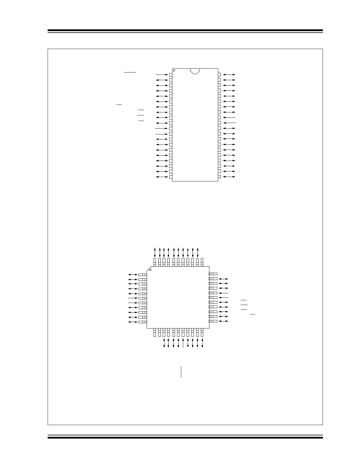
Pin Diagrams
PIC
1
8F
252
3
10
11
2
3
4
5
6
1
8
7
9
12
13
14
15
16
17
18
19
20
23
24
25
26
27
28
22
21
MCLR/V
PP
/RE3
RA0/AN0
RA1/AN1
RA2/AN2/V
REF
-/CV
REF
RA3/AN3/V
REF
+
RA4/T0CKI/C1OUT
RA5/AN4/SS/HLVDIN/C2OUT
V
SS
OSC1/CLKI
(3)
/RA7
OSC2/CLKO
(3)
/RA6
RC0/T1OSO/T13CKI
RC1/T1OSI/CCP2
(2)
RC2/CCP1
RC3/SCK/SCL
RB7/KBI3/PGD
RB6//KBI2/PGC
RB5/KBI1/PGM
RB4/KBI0/AN11
RB3/AN9/CCP2
(2)
RB2/INT2/AN8
RB1/INT1/AN10
RB0/INT0/FLT0/AN12
V
DD
V
SS
RC7/RX/DT
RC6/TX/CK
RC5/SDO
RC4/SDI/SDA
28-Pin PDIP, SOIC
PIC
1
8F
242
3
Note 1:
It is recommended to connect the bottom pad of QFN package parts to V
SS
.
2:
RB3 is the alternate pin for CCP2 multiplexing.
3:
OSC1/CLKI and OSC2/CLKO are only available in select oscillator modes and when these pins are not
being used as digital I/O. For additional information, see Section 2.0 “Oscillator Configurations” of the
“PIC18F2420/2520/4420/4520 Data Sheet” (DS39631).
10 11
2
3
6
1
18
19
20
21
22
12 13 14
15
8
7
16
17
23
24
25
26
27
28
9
PIC18F2423
R
C
0/T
1OS
O
/T1
3C
K
I
5
4
RB7
/KBI
3
/PG
D
RB6
/KBI
2
/PG
C
RB5
/KBI
1
/PG
M
RB4
KBI
0
/AN1
1
RB3/AN9/CCP2
(2)
RB2/INT2/AN8
RB1/INT1/AN10
RB0/INT0/FLT0/AN12
V
DD
V
SS
RC7/RX/DT
RC6
/T
X
/CK
RC5
/SDO
RC4
/S
DI
/SDA
MC
LR
/V
PP
/RE
3
RA0
/A
N
0
RA1
/A
N
1
RA2/AN2/V
REF
-/CV
REF
RA3/AN3/V
REF
+
RA4/T0CKI/C1OUT
RA5/AN4/SS/HLVDIN/C2OUT
V
SS
OSC1/CLKI
(3)
/RA7
OSC2/CLKO
(3)
/RA6
RC1
/T
1
O
SI/CCP2
(2
)
RC2
/CCP1
RC3
/SCK/SCL
PIC18F2523
28-Pin QFN
(1)
© 2009 Microchip Technology Inc.
DS39755C-page 5
PIC18F2423/2523/4423/4523
Pin Diagrams (Continued)
RB7/KBI3/PGD
RB6/KBI2/PGC
RB5/KBI1/PGM
RB4/KBI0/AN11
RB3/AN9/CCP2
(1)
RB2/INT2/AN8
RB1/INT1/AN10
RB0/INT0/FLT0/AN12
V
DD
V
SS
RD7/PSP7/P1D
RD6/PSP6/P1C
RD5/PSP5/P1B
RD4/PSP4
RC7/RX/DT
RC6/TX/CK
RC5/SDO
RC4/SDI/SDA
RD3/PSP3
RD2/PSP2
MCLR/V
PP
/RE3
RA0/AN0
RA1/AN1
RA2/AN2/V
REF
-/CV
REF
RA3/AN3/V
REF
+
RA4/T0CKI/C1OUT
RA5/AN4/SS/HLVDIN/C2OUT
RE0/RD/AN5
RE1/WR/AN6
RE2/CS/AN7
V
DD
V
SS
OSC1/CLKI
(2)
/RA7
OSC2/CLKO
(2)
/RA6
RC0/T1OSO/T13CKI
RC1/T1OSI/CCP2
(1)
RC2/CCP1/P1A
RC3/SCK/SCL
RD0/PSP0
RD1/PSP1
1
2
3
4
5
6
7
8
9
10
11
12
13
14
15
16
17
18
19
20
40
39
38
37
36
35
34
33
32
31
30
29
28
27
26
25
24
23
22
21
PIC
1
8F
452
3
40-Pin PDIP
PIC
1
8F
442
3
10
11
2
3
4
5
6
1
18
19
20
21 22
12
13
14
15
38
8
7
44
43
42 41
40
39
16
17
29
30
31
32
33
23
24
25
26
27
28
36
34
35
9
PIC18F4423
37
RA
3
/AN3
/V
RE
F
+
RA2
/AN
2/
V
RE
F
-/C
V
RE
F
RA
1
/AN1
RA
0
/AN0
MC
L
R
/V
PP
/RE
3
NC
RB
7/
K
B
I3
/P
GD
RB
6/
K
B
I2
/P
GC
RB5
/KBI
1/
PG
M
RB
4/
K
B
I0
/A
N1
1
NC
RC
6/
T
X
/CK
RC
5/
SDO
RC
4/
SDI/SDA
RD
3/
PSP3
RD
2/
PSP2
RD
1/
PSP1
RD
0/
PSP0
RC
3/
SCK/
SCL
RC
2/
CCP1
/P
1
A
RC1/T
1OS
I/C
C
P
2
(1
)
NC
NC
RC0/T1OSO/T13CKI
OSC2/CLKO
(2)
/RA6
OSC1/CLKI
(2)
/RA7
V
SS
V
DD
RE2/CS/AN7
RE1/WR/AN6
RE0/RD/AN5
RA5/AN4/SS/HLVDIN/C2OUT
RA4/T0CKI/C1OUT
RC7/RX/DT
RD4/PSP4
RD5/PSP5/P1B
RD6/PSP6/P1C
RD7/PSP7/P1D
V
SS
V
DD
RB0/INT0/FLT0/AN12
RB1/INT1/AN10
RB2/INT2/AN8
RB3/AN9/CCP2
(1)
44-Pin TQFP
PIC18F4523
Note 1:
RB3 is the alternate pin for CCP2 multiplexing.
2:
OSC1/CLKI and OSC2/CLKO are only available in select oscillator modes and when these pins are not
being used as digital I/O. For additional information, see Section 2.0 “Oscillator Configurations” of the
“PIC18F2420/2520/4420/4520 Data Sheet” (DS39631).
PIC18F2423/2523/4423/4523
DS39755C-page 6
© 2009 Microchip Technology Inc.
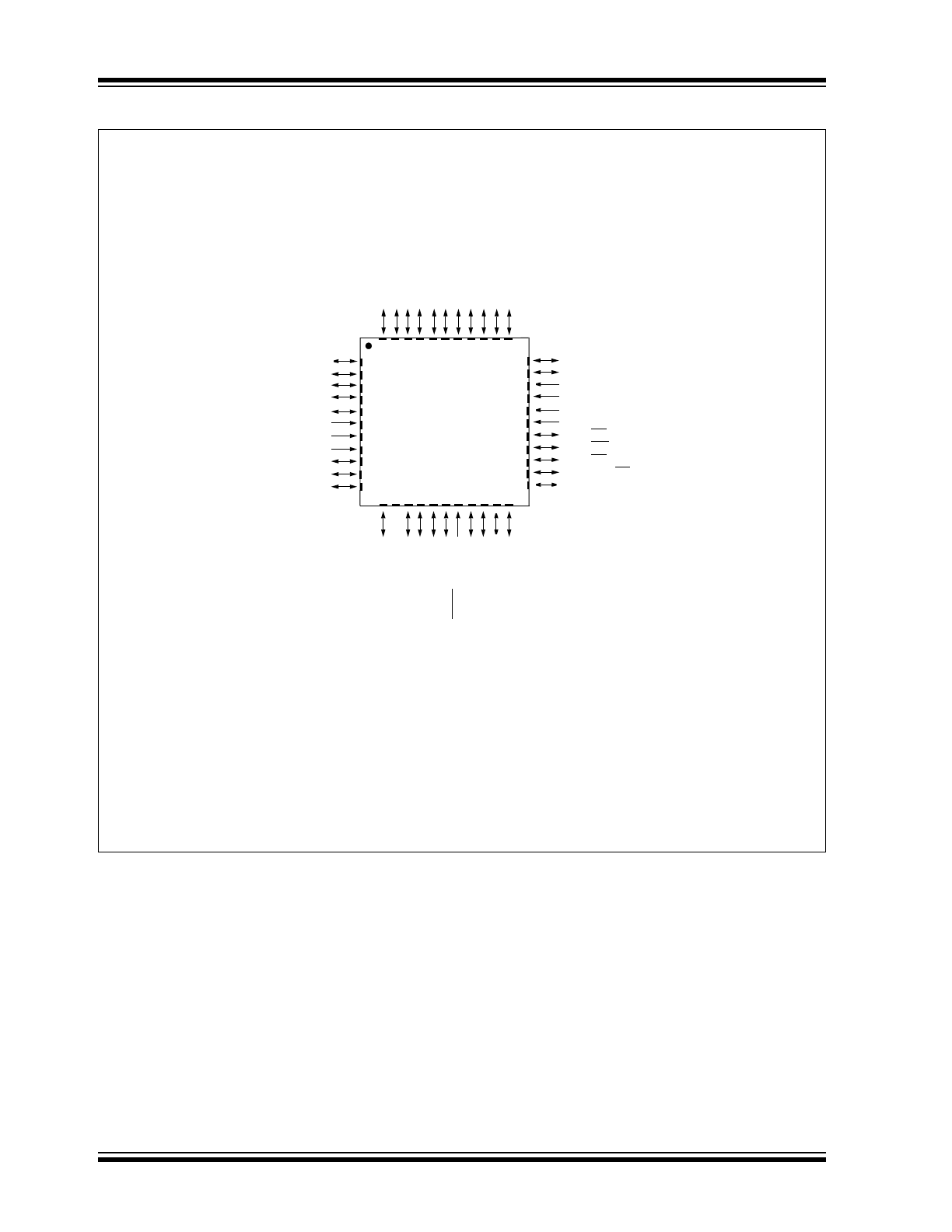
Pin Diagrams (Continued)
10
11
2
3
4
5
6
1
18
19
20
21 22
12 13
14
15
38
8
7
44
43
42 41
40
39
16
17
29
30
31
32
33
23
24
25
26
27
28
36
34
35
9
PIC18F4423
37
RA3
/AN3
/V
RE
F
+
R
A
2/A
N
2/V
RE
F
-/
C
V
RE
F
RA1
/AN1
RA0
/AN0
MC
LR
/V
PP
/RE
3
RB
3
/A
N
9/
C
C
P
2
(2
)
R
B
7
/KBI
3/
PG
D
R
B
6
/KBI
2/
PG
C
RB5
/KBI
1
/PG
M
RB4
/KBI
0/
AN1
1
NC
RC6
/T
X
/CK
RC5
/SDO
RC4
/SDI/SDA
RD3
/PSP3
RD2
/PSP2
RD1
/PSP1
RD0
/PSP0
RC3
/SCK/SCL
RC2
/CCP1
/P1
A
RC1
/T
1OS
I/C
CP
2
(2
)
RC0/T
1OS
O/T
13
CK
I
OSC2/CLKO
(3)
/RA6
OSC1/CLKI
(3)
/RA7
V
SS
V
SS
V
DD
V
DD
RE2/CS/AN7
RE1/WR/AN6
RE0/RD/AN5
RA5/AN4/SS/HLVDIN/C2OUT
RA4/T0CKI/C1OUT
RC7/RX/DT
RD4/PSP4
RD5/PSP5/P1B
RD6/PSP6/P1C
RD7/PSP7/P1D
V
SS
V
DD
V
DD
RB0/INT0/FLT0/AN12
RB1/INT1/AN10
RB2/INT2/AN8
44-Pin QFN
(1)
PIC18F4523
Note 1:
It is recommended to connect the bottom pad of QFN package parts to V
SS
.
2:
RB3 is the alternate pin for CCP2 multiplexing.
3:
OSC1/CLKI and OSC2/CLKO are only available in select oscillator modes and when these pins are not
being used as digital I/O. For additional information, see Section 2.0 “Oscillator Configurations” of the
“PIC18F2420/2520/4420/4520 Data Sheet” (DS39631).

© 2009 Microchip Technology Inc.
DS39755C-page 7
PIC18F2423/2523/4423/4523
Table of Contents
1.0
Device Overview .......................................................................................................................................................................... 9
2.0
12-Bit Analog-to-Digital Converter (A/D) Module ....................................................................................................................... 25
3.0
Special Features of the CPU...................................................................................................................................................... 35
4.0
Electrical Characteristics ............................................................................................................................................................ 37
5.0
Packaging Information................................................................................................................................................................ 43
Appendix A: Revision History............................................................................................................................................................... 45
Appendix B: Device Differences .......................................................................................................................................................... 45
Appendix C: Conversion Considerations ............................................................................................................................................. 46
Appendix D: Migration from Baseline to Enhanced Devices................................................................................................................ 46
Appendix E: Migration from Mid-Range to Enhanced Devices ............................................................................................................ 47
Appendix F: Migration from High-End to Enhanced Devices............................................................................................................... 47
Index ................................................................................................................................................................................................... 49
The Microchip Web Site....................................................................................................................................................................... 51
Customer Change Notification Service ................................................................................................................................................ 51
Customer Support................................................................................................................................................................................ 51
Reader Response ................................................................................................................................................................................ 52
Product Identification System .............................................................................................................................................................. 53

PIC18F2423/2523/4423/4523
DS39755C-page 8
© 2009 Microchip Technology Inc.
TO OUR VALUED CUSTOMERS
It is our intention to provide our valued customers with the best documentation possible to ensure successful use of your Microchip
products. To this end, we will continue to improve our publications to better suit your needs. Our publications will be refined and
enhanced as new volumes and updates are introduced.
If you have any questions or comments regarding this publication, please contact the Marketing Communications Department via
E-mail at docerrors@microchip.com or fax the Reader Response Form in the back of this data sheet to (480) 792-4150. We
welcome your feedback.
Most Current Data Sheet
To obtain the most up-to-date version of this data sheet, please register at our Worldwide Web site at:
http://www.microchip.com
You can determine the version of a data sheet by examining its literature number found on the bottom outside corner of any page.
The last character of the literature number is the version number, (e.g., DS30000A is version A of document DS30000).
Errata
An errata sheet, describing minor operational differences from the data sheet and recommended workarounds, may exist for current
devices. As device/documentation issues become known to us, we will publish an errata sheet. The errata will specify the revision
of silicon and revision of document to which it applies.
To determine if an errata sheet exists for a particular device, please check with one of the following:
• Microchip’s Worldwide Web site; http://www.microchip.com
• Your local Microchip sales office (see last page)
When contacting a sales office, please specify which device, revision of silicon and data sheet (include literature number) you are
using.
Customer Notification System
Register on our web site at www.microchip.com to receive the most current information on all of our products.

© 2009 Microchip Technology Inc.
DS39755C-page 9
PIC18F2423/2523/4423/4523
1.0
DEVICE OVERVIEW
This document contains device-specific information for
the following devices:
This family offers the advantages of all PIC18
microcontrollers – namely, high computational perfor-
mance at an economical price – with the addition of
high-endurance, Enhanced Flash program memory.
On top of these features, the PIC18F2423/2523/4423/
4523 family introduces design enhancements that
make these microcontrollers a logical choice for many
high-performance, power-sensitive applications.
1.1
New Core Features
1.1.1
nanoWatt TECHNOLOGY
All of the devices in the PIC18F2423/2523/4423/4523
family incorporate a range of features that can signifi-
cantly reduce power consumption during operation.
Key items include:
• Alternate Run Modes: By clocking the controller
from the Timer1 source or the internal oscillator
block, power consumption during code execution
can be reduced by as much as 90%.
• Multiple Idle Modes: The controller also can run
with its CPU core disabled and the peripherals still
active. In these states, power consumption can be
reduced even further, to as little as 4% of normal
operation requirements.
• On-the-Fly Mode Switching: The power-managed
modes are invoked by user code during operation,
allowing the user to incorporate power-saving ideas
into their application’s software design.
• Low Consumption in Key Modules: The power
requirements for both Timer1 and the Watchdog
Timer are minimized. See Section 4.0 “Electrical
Characteristics” for values.
1.1.2
MULTIPLE OSCILLATOR OPTIONS
AND FEATURES
All of the devices in the PIC18F2423/2523/4423/4523
family offer ten different oscillator options, allowing
users a wide range of choices in developing application
hardware. These include:
• Four Crystal modes, using crystals or ceramic
resonators.
• Two External Clock modes, offering the option of
using two pins (oscillator input and a divide-by-4
clock output) or one pin (oscillator input, with the
second pin reassigned as general I/O).
• Two External RC Oscillator modes with the same
pin options as the External Clock modes.
• An internal oscillator block that offers eight clock
frequencies: an 8 MHz clock and an INTRC source
(approximately 31 kHz), as well as a range of six
user-selectable clock frequencies, between
125 kHz to 4 MHz. This option frees the two
oscillator pins for use as additional general
purpose I/O.
• A Phase Lock Loop (PLL) frequency multiplier,
available to both the High-Speed Crystal and
Internal Oscillator modes, allowing clock speeds
of up to 40 MHz from the HS clock source. Used
with the internal oscillator, the PLL gives users a
complete selection of clock speeds, from 31 kHz
to 32 MHz, all without using an external crystal or
clock circuit.
Besides its availability as a clock source, the internal
oscillator block provides a stable reference source that
gives the family additional features for robust
operation:
• Fail-Safe Clock Monitor: Constantly monitors
the main clock source against a reference signal
provided by the internal oscillator. If a clock failure
occurs, the controller is switched to the internal
oscillator block, allowing for continued operation
or a safe application shutdown.
• Two-Speed Start-up: Allows the internal oscillator
to serve as the clock source from Power-on Reset,
or wake-up from Sleep mode, until the primary clock
source is available.
• PIC18F2423
• PIC18LF2423
• PIC18F2523
• PIC18LF2523
• PIC18F4423
• PIC18LF4423
• PIC18F4523
• PIC18LF4523
Note: This data sheet documents only the devices’
features and specifications that are in addition
to, or different from, the features and specifi-
cations of the PIC18F2420/2520/4420/4520
devices. For information on the features and
specifications shared by the PIC18F2423/
2523/4423/4523 and PIC18F2420/2520/
4420/4520 devices, see the “PIC18F2420/
2520/4420/4520 Data Sheet” (DS39631).

PIC18F2423/2523/4423/4523
DS39755C-page 10
© 2009 Microchip Technology Inc.
1.2
Other Special Features
• 12-Bit A/D Converter: This module incorporates
programmable acquisition time, allowing for a
channel to be selected and a conversion to be
initiated without waiting for a sampling period,
thereby reducing code overhead.
• Memory Endurance: The Enhanced Flash cells
for both program memory and data EEPROM are
rated to last for many thousands of erase/write
cycles – up to 100,000 for program memory and
1,000,000 for EEPROM. Data retention without
refresh is conservatively estimated to be greater
than 40 years.
• Self-Programmability: These devices can write
to their own program memory spaces under inter-
nal software control. By using a bootloader routine
located in the protected Boot Block at the top of
program memory, it is possible to create an
application that can update itself in the field.
• Extended Instruction Set: The PIC18F2423/
2523/4423/4523 family introduces an optional
extension to the PIC18 instruction set that adds
eight new instructions and an Indexed Addressing
mode. This extension, enabled as a device con-
figuration option, has been specifically designed
to optimize re-entrant application code originally
developed in high-level languages, such as C.
• Enhanced CCP module: In PWM mode, this
module provides one, two or four modulated
outputs for controlling half-bridge and full-bridge
drivers. Other features include auto-shutdown, for
disabling PWM outputs on interrupt or other select
conditions, and auto-restart, to reactivate outputs
once the condition has cleared.
• Enhanced Addressable USART: This serial
communication module is capable of standard
RS-232 operation and provides support for the
LIN/J2602 bus protocol. Other enhancements
include automatic baud rate detection and a 16-bit
Baud Rate Generator for improved resolution.
When the microcontroller is using the internal
oscillator block, the EUSART provides stable
operation for applications that talk to the outside
world without using an external crystal (or its
accompanying power requirement).
• Extended Watchdog Timer (WDT): This
Enhanced version incorporates a 16-bit prescaler,
allowing an extended time-out range that is stable
across operating voltage and temperature. See
Section 4.0 “Electrical Characteristics” for
time-out periods.
1.3
Details on Individual Family
Members
Devices in the PIC18F2423/2523/4423/4523 family are
available in 28-pin and 40/44-pin packages. Block
diagrams for the two groups are shown in Figure 1-1
and Figure 1-2.
The devices are differentiated from each other in these
ways:
• Flash Program Memory:
- PIC18F2423/4423 devices – 16 Kbytes
- PIC18F2523/4523 devices – 32 Kbytes
• A/D Channels:
- PIC18F2423/2523 devices – 10
- PIC18F4423/4523 devices – 13
• I/O Ports:
- PIC18F2423/2523 devices – Three bidirectional
ports
- PIC18F4423/4523 devices – Five bidirectional
ports
• CCP and Enhanced CCP Implementation:
- PIC18F2423/2523 devices – Two standard
CCP modules
- PIC18F4423/4523 devices – One standard
CCP module and one ECCP module
• Parallel Slave Port – Present only on
PIC18F4423/4523 devices
All other features for devices in this family are identical.
These are summarized in Table 1-1.
The pinouts for all devices are listed in Table 1-2 and
Table 1-3.
Members of the PIC18F2423/2523/4423/4523 family
are available only as low-voltage devices, designated
by “LF” (such as PIC18LF2423), and function over an
extended V
DD
range of 2.0V to 5.5V.