
1996 Microchip Technology Inc.
DS30412C-page 1
Devices included in this data sheet:
• PIC17CR42
• PIC17C42A
• PIC17C43
• PIC17CR43
• PIC17C44
• PIC17C42†
Microcontroller Core Features:
• Only 58 single word instructions to learn
• All single cycle instructions (121 ns) except for
program branches and table reads/writes which
are two-cycle
• Operating speed:
- DC - 33 MHz clock input
- DC - 121 ns instruction cycle
• Hardware Multiplier
(Not available on the PIC17C42)
• Interrupt capability
• 16 levels deep hardware stack
• Direct, indirect and relative addressing modes
• Internal/External program memory execution
• 64K x 16 addressable program memory space
Peripheral Features:
• 33 I/O pins with individual direction control
• High current sink/source for direct LED drive
- RA2 and RA3 are open drain, high voltage
(12V), high current (60 mA), I/O
• Two capture inputs and two PWM outputs
- Captures are 16-bit, max resolution 160 ns
- PWM resolution is 1- to 10-bit
• TMR0: 16-bit timer/counter with 8-bit programma-
ble prescaler
• TMR1: 8-bit timer/counter
Device
Program Memory
Data Memory
EPROM
ROM
PIC17CR42
-
2K
232
PIC17C42A
2K
-
232
PIC17C43
4K
-
454
PIC17CR43
-
4K
454
PIC17C44
8K
-
454
PIC17C42†
2K
-
232
✯
✯
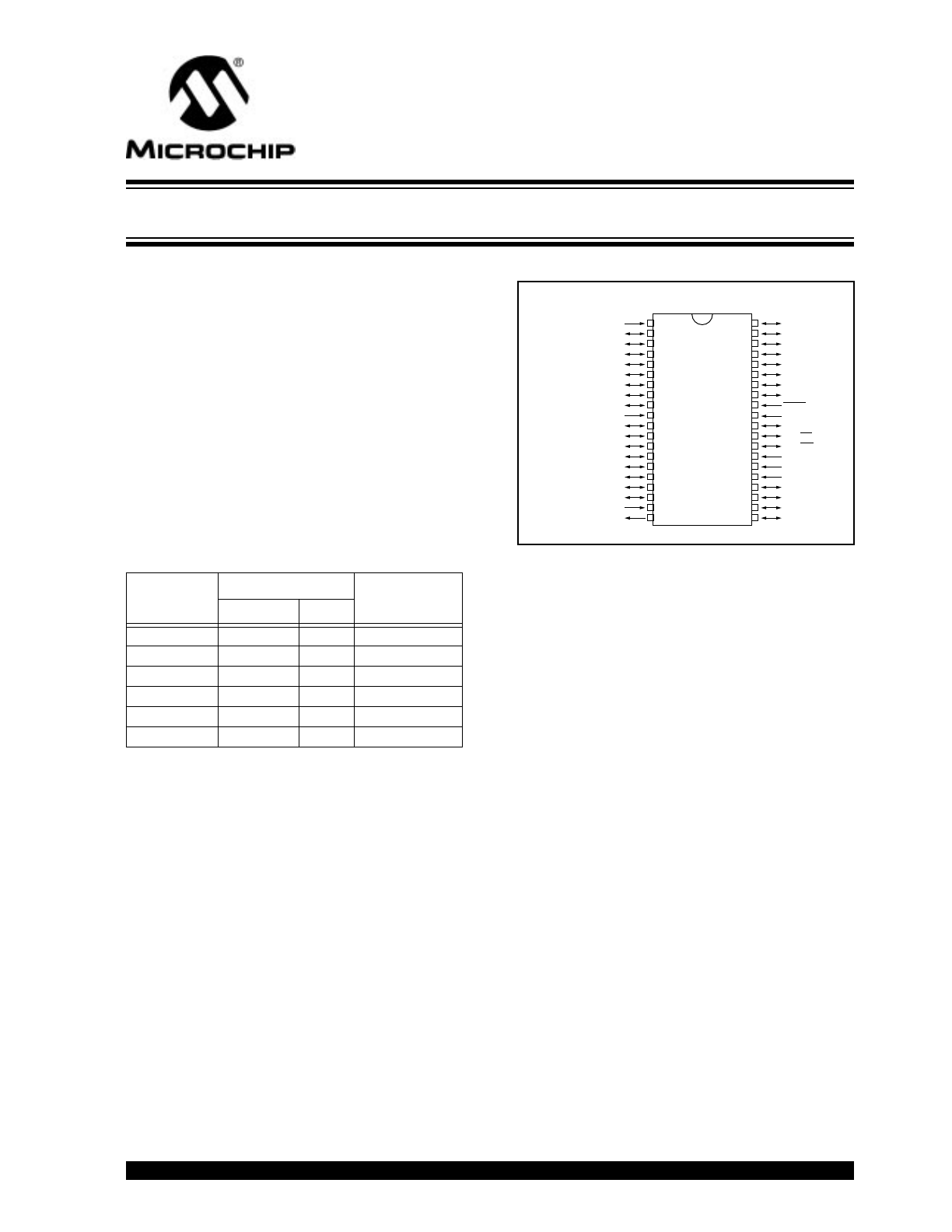
Pin Diagram
• TMR2: 8-bit timer/counter
• TMR3: 16-bit timer/counter
• Universal Synchronous Asynchronous Receiver
Transmitter (USART/SCI)
Special Microcontroller Features:
• Power-on Reset (POR), Power-up Timer (PWRT)
and Oscillator Start-up Timer (OST)
• Watchdog Timer (WDT) with its own on-chip RC
oscillator for reliable operation
• Code-protection
• Power saving SLEEP mode
• Selectable oscillator options
CMOS Technology:
• Low-power, high-speed CMOS EPROM/ROM
technology
• Fully static design
• Wide operating voltage range (2.5V to 6.0V)
• Commercial and Industrial Temperature Range
• Low-power consumption
- < 5 mA @ 5V, 4 MHz
- 100
µ
A typical @ 4.5V, 32 kHz
- < 1
µ
A typical standby current @ 5V
PIC17C4X
RD0/AD8
RD1/AD9
RD2/AD10
RD3/AD11
RD4/AD12
RD5/AD13
RD6/AD14
RD7/AD15
MCLR/V
PP
V
SS
RE0/ALE
RE1/OE
RE2/WR
TEST
RA0/INT
RA1/T0CKI
RA2
RA3
RA4/RX/DT
RA5/TX/CK
V
DD
RC0/AD0
RC1/AD1
RC2/AD2
RC3/AD3
RC4/AD4
RC5/AD5
RC6/AD6
RC7/AD7
V
SS
RB0/CAP1
RB1/CAP2
RB2/PWM1
RB3/PWM2
RB4/TCLK12
RB5/TCLK3
RB6
RB7
OSC1/CLKIN
OSC2/CLKOUT
1
2
3
4
5
6
7
8
9
10
11
12
13
14
15
16
17
18
19
20
40
39
38
37
36
35
34
33
32
31
30
29
28
27
26
25
24
23
22
21
PDIP, CERDIP, Windowed CERDIP
PIC17C4X
High-Performance 8-Bit CMOS EPROM/ROM Microcontroller
†NOT recommended for new designs, use 17C42A.
This document was created with FrameMaker 4 0 4
PIC17C4X
DS30412C-page 2
1996 Microchip Technology Inc.
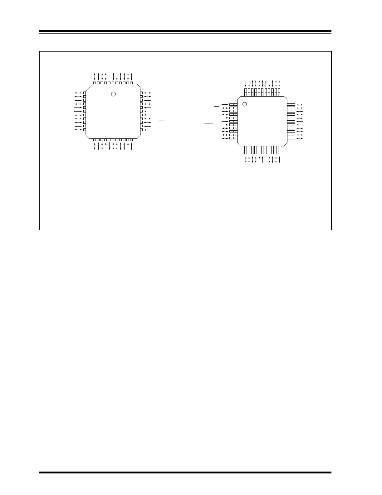
Pin Diagrams Cont.’d
RD4/AD12
RD5/AD13
RD6/AD14
RD7/AD15
MCLR/V
PP
V
SS
V
SS
RE0/ALE
RE1/OE
RE2/WR
TEST
RC4/AD4
RC5/AD5
RC6/AD6
RC7/AD7
V
SS
V
SS
RB0/CAP1
RB1/CAP2
RB2/PWM1
RB3/PWM2
RB4/TCLK12
RC3/AD3
RC2/AD2
RC1/AD1
RC0/AD0
NC
V
DD
V
DD
RD0/AD8
RD1/AD9
RD2/AD10
RD3/AD11
7
8
9
10
11
12
13
14
15
16
17
39
38
37
36
35
34
33
32
31
30
29
RA0/INT
RA1/T0CKI
RA2
RA3
RA4/RX/DT
RA5/TX/CK
OSC2/CLK
OUT
OSC1/CLKIN
RB7
RB6
RB5/TCLK3
6
5
4
3
2
1
44
43
42
41
40
28
27
26
25
24
23
22
21
20
19
18
RB4/TCLK12
RB3/PWM2
RB2/PWM1
RB1/CAP2
RB0/CAP1
V
SS
V
SS
RC7/AD7
RC6/AD6
RC5/AD5
RC4/AD4
TEST
RE2/WR
RE1/OE
RE0/ALE
V
SS
V
SS
MCLR/V
PP
RD7/AD15
RD6/AD14
RD5/AD13
RD4/AD12
RA0/INT
RA1/T0CKI
RA2
RA3
RA4/RX/DT
RA5/TX/CK
OSC2/CLK
OUT
OSC1/CLKIN
RB7
RB6
RB5/TCLK3
1
2
3
4
5
6
7
8
9
10
11
33
32
31
30
29
28
27
26
25
24
23
RC3/AD3
RC2/AD2
RC1/AD1
RC0/AD0
NC
V
DD
V
DD
RD0/AD8
RD1/AD9
RD2/AD10
RD3/AD11
44
43
42
41
40
39
38
37
36
35
34
22
21
20
19
18
17
16
15
14
13
12
PLCC
MQFP
TQFP
All devices are available in all package types, listed in Section 21.0, with the following exceptions:
• ROM devices are not available in Windowed CERDIP Packages
• TQFP is not available for the PIC17C42.
PIC17C4X
PIC17C4X
1996 Microchip Technology Inc.
DS30412C-page 3
PIC17C4X
Table of Contents
1.0
Overview .............................................................................................................................................................. 5
2.0
PIC17C4X Device Varieties ................................................................................................................................. 7
3.0
Architectural Overview ......................................................................................................................................... 9
4.0
Reset .................................................................................................................................................................. 15
5.0
Interrupts ............................................................................................................................................................ 21
6.0
Memory Organization ......................................................................................................................................... 29
7.0
Table Reads and Table Writes........................................................................................................................... 43
8.0
Hardware Multiplier ............................................................................................................................................ 49
9.0
I/O Ports ............................................................................................................................................................. 53
10.0
Overview of Timer Resources ............................................................................................................................ 65
11.0
Timer0 ................................................................................................................................................................ 67
12.0
Timer1, Timer2, Timer3, PWMs and Captures................................................................................................... 71
13.0
Universal Synchronous Asynchronous Receiver Transmitter (USART) Module ................................................ 83
14.0
Special Features of the CPU.............................................................................................................................. 99
15.0
Instruction Set Summary .................................................................................................................................. 107
16.0
Development Support....................................................................................................................................... 143
17.0
PIC17C42 Electrical Characteristics ................................................................................................................ 147
18.0
PIC17C42 DC and AC Characteristics............................................................................................................. 163
19.0
PIC17CR42/42A/43/R43/44 Electrical Characteristics..................................................................................... 175
20.0
PIC17CR42/42A/43/R43/44 DC and AC Characteristics ................................................................................. 193
21.0
Packaging Information...................................................................................................................................... 205
Appendix A: Modifications .......................................................................................................................................... 211
Appendix B: Compatibility........................................................................................................................................... 211
Appendix C: What’s New ............................................................................................................................................ 212
Appendix D: What’s Changed..................................................................................................................................... 212
Appendix E: PIC16/17 Microcontrollers ...................................................................................................................... 213
Appendix F: Errata for PIC17C42 Silicon ................................................................................................................... 223
Index ............................................................................................................................................................................ 226
PIC17C4X Product Identification System .................................................................................................................... 237
For register and module descriptions in this data sheet, device legends show which devices apply to those sections.
For example, the legend below shows that some features of only the PIC17C43, PIC17CR43, PIC17C44 are described
in this section.
Applicable Devices
42 R42 42A 43 R43 44
To Our Valued Customers
We constantly strive to improve the quality of all our products and documentation. We have spent an excep-
tional amount of time to ensure that these documents are correct. However, we realize that we may have
missed a few things. If you find any information that is missing or appears in error from the previous version of
the PIC17C4X Data Sheet (Literature Number DS30412B), please use the reader response form in the back
of this data sheet to inform us. We appreciate your assistance in making this a better document.
To assist you in the use of this document, Appendix C contains a list of new information in this data sheet,
while Appendix D contains information that has changed

PIC17C4X
DS30412C-page 4
1996 Microchip Technology Inc.
NOTES:

1996 Microchip Technology Inc.
DS30412C-page 5
PIC17C4X
1.0
OVERVIEW
This data sheet covers the PIC17C4X group of the
PIC17CXX family of microcontrollers. The following
devices are discussed in this data sheet:
• PIC17C42
• PIC17CR42
• PIC17C42A
• PIC17C43
• PIC17CR43
• PIC17C44
The PIC17CR42, PIC17C42A, PIC17C43,
PIC17CR43, and PIC17C44 devices include architec-
tural enhancements over the PIC17C42. These
enhancements will be discussed throughout this data
sheet.
The PIC17C4X devices are 40/44-Pin,
EPROM/ROM-based members of the versatile
PIC17CXX family of low-cost, high-performance,
CMOS, fully-static, 8-bit microcontrollers.
All PIC16/17 microcontrollers employ an advanced
RISC architecture. The PIC17CXX has enhanced core
features, 16-level deep stack, and multiple internal and
external interrupt sources. The separate instruction and
data buses of the Harvard architecture allow a 16-bit
wide instruction word with a separate 8-bit wide data.
The two stage instruction pipeline allows all instructions
to execute in a single cycle, except for program
branches (which require two cycles). A total of 55
instructions (reduced instruction set) are available in
the PIC17C42 and 58 instructions in all the other
devices. Additionally, a large register set gives some of
the architectural innovations used to achieve a very
high performance. For mathematical intensive applica-
tions all devices, except the PIC17C42, have a single
cycle 8 x 8 Hardware Multiplier.
PIC17CXX microcontrollers typically achieve a 2:1
code compression and a 4:1 speed improvement over
other 8-bit microcontrollers in their class.
PIC17C4X devices have up to 454 bytes of RAM and
33 I/O pins. In addition, the PIC17C4X adds several
peripheral features useful in many high performance
applications including:
• Four timer/counters
• Two capture inputs
• Two PWM outputs
• A Universal Synchronous Asynchronous Receiver
Transmitter (USART)
These special features reduce external components,
thus reducing cost, enhancing system reliability and
reducing power consumption. There are four oscillator
options, of which the single pin RC oscillator provides a
low-cost solution, the LF oscillator is for low frequency
crystals and minimizes power consumption, XT is a
standard crystal, and the EC is for external clock input.
The SLEEP (power-down) mode offers additional
power saving. The user can wake-up the chip from
SLEEP through several external and internal interrupts
and device resets.
There are four configuration options for the device oper-
ational modes:
• Microprocessor
• Microcontroller
• Extended microcontroller
• Protected microcontroller
The microprocessor and extended microcontroller
modes allow up to 64K-words of external program
memory.
A highly reliable Watchdog Timer with its own on-chip
RC oscillator provides protection against software mal-
function.
Table 1-1 lists the features of the PIC17C4X devices.
A UV-erasable CERDIP-packaged version is ideal for
code development while the cost-effective One-Time
Programmable (OTP) version is suitable for production
in any volume.
The PIC17C4X fits perfectly in applications ranging
from precise motor control and industrial process con-
trol to automotive, instrumentation, and telecom appli-
cations. Other applications that require extremely fast
execution of complex software programs or the flexibil-
ity of programming the software code as one of the last
steps of the manufacturing process would also be well
suited. The EPROM technology makes customization
of application programs (with unique security codes,
combinations, model numbers, parameter storage,
etc.) fast and convenient. Small footprint package
options make the PIC17C4X ideal for applications with
space limitations that require high performance. High
speed execution, powerful peripheral features, flexible
I/O, and low power consumption all at low cost make
the PIC17C4X ideal for a wide range of embedded con-
trol applications.
1.1
Family and Upward Compatibility
Those users familiar with the PIC16C5X and
PIC16CXX families of microcontrollers will see the
architectural enhancements that have been imple-
mented. These enhancements allow the device to be
more efficient in software and hardware requirements.
Please refer to Appendix A for a detailed list of
enhancements and modifications. Code written for
PIC16C5X or PIC16CXX can be easily ported to
PIC17CXX family of devices (Appendix B).
1.2
Development Support
The PIC17CXX family is supported by a full-featured
macro assembler, a software simulator, an in-circuit
emulator, a universal programmer, a “C” compiler, and
fuzzy logic support tools.
This document was created with FrameMaker 4 0 4
PIC17C4X
DS30412C-page 6
1996 Microchip Technology Inc.
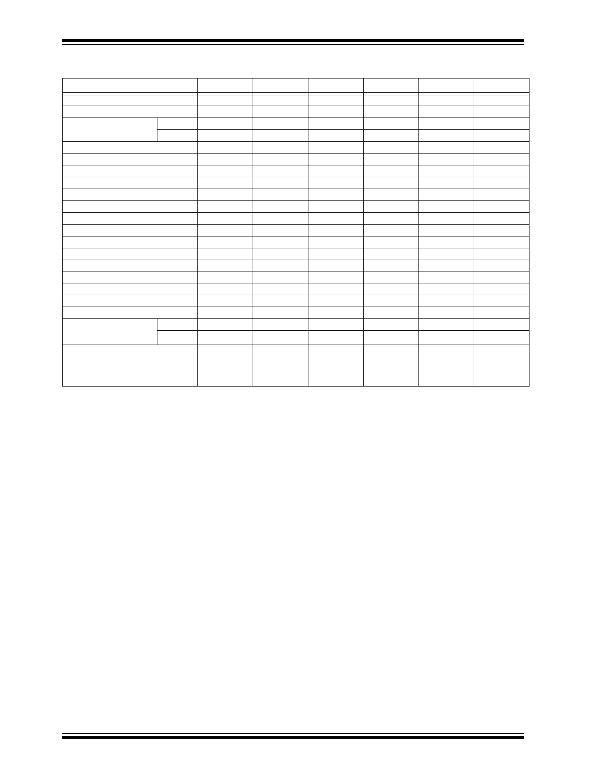
TABLE 1-1:
PIC17CXX FAMILY OF DEVICES
Features
PIC17C42
PIC17CR42
PIC17C42A
PIC17C43
PIC17CR43
PIC17C44
Maximum Frequency of Operation
25 MHz
33 MHz
33 MHz
33 MHz
33 MHz
33 MHz
Operating Voltage Range
4.5 - 5.5V
2.5 - 6.0V
2.5 - 6.0V
2.5 - 6.0V
2.5 - 6.0V
2.5 - 6.0V
Program Memory x16
(EPROM)
2K
-
2K
4K
-
8K
(ROM)
-
2K
-
-
4K
-
Data Memory (bytes)
232
232
232
454
454
454
Hardware Multiplier (8 x 8)
-
Yes
Yes
Yes
Yes
Yes
Timer0 (16-bit + 8-bit postscaler)
Yes
Yes
Yes
Yes
Yes
Yes
Timer1 (8-bit)
Yes
Yes
Yes
Yes
Yes
Yes
Timer2 (8-bit)
Yes
Yes
Yes
Yes
Yes
Yes
Timer3 (16-bit)
Yes
Yes
Yes
Yes
Yes
Yes
Capture inputs (16-bit)
2
2
2
2
2
2
PWM outputs (up to 10-bit)
2
2
2
2
2
2
USART/SCI
Yes
Yes
Yes
Yes
Yes
Yes
Power-on Reset
Yes
Yes
Yes
Yes
Yes
Yes
Watchdog Timer
Yes
Yes
Yes
Yes
Yes
Yes
External Interrupts
Yes
Yes
Yes
Yes
Yes
Yes
Interrupt Sources
11
11
11
11
11
11
Program Memory Code Protect
Yes
Yes
Yes
Yes
Yes
Yes
I/O Pins
33
33
33
33
33
33
I/O High Current Capabil-
ity
Source
25 mA
25 mA
25 mA
25 mA
25 mA
25 mA
Sink
25 mA
(1)
25 mA
(1)
25 mA
(1)
25 mA
(1)
25 mA
(1)
25 mA
(1)
Package Types
40-pin DIP
44-pin PLCC
44-pin MQFP
40-pin DIP
44-pin PLCC
44-pin MQFP
44-pin TQFP
40-pin DIP
44-pin PLCC
44-pin MQFP
44-pin TQFP
40-pin DIP
44-pin PLCC
44-pin MQFP
44-pin TQFP
40-pin DIP
44-pin PLCC
44-pin MQFP
44-pin TQFP
40-pin DIP
44-pin PLCC
44-pin MQFP
44-pin TQFP
Note 1:
Pins RA2 and RA3 can sink up to 60 mA.

1996 Microchip Technology Inc.
DS30412C-page 7
PIC17C4X
2.0
PIC17C4X DEVICE VARIETIES
A variety of frequency ranges and packaging options
are available. Depending on application and production
requirements, the proper device option can be selected
using the information in the PIC17C4X Product Selec-
tion System section at the end of this data sheet. When
placing orders, please use the “PIC17C4X Product
Identification System” at the back of this data sheet to
specify the correct part number.
For the PIC17C4X family of devices, there are four
device “types” as indicated in the device number:
1.
C
, as in PIC17
C
42. These devices have
EPROM type memory and operate over the
standard voltage range.
2.
LC
, as in PIC17
LC
42. These devices have
EPROM type memory, operate over an
extended voltage range, and reduced frequency
range.
3.
CR
, as in PIC17
CR
42. These devices have
ROM type memory and operate over the stan-
dard voltage range.
4.
LCR
, as in PIC17
LCR
42. These devices have
ROM type memory, operate over an extended
voltage range, and reduced frequency range.
2.1
UV Erasable Devices
The UV erasable version, offered in CERDIP package,
is optimal for prototype development and pilot pro-
grams.
The UV erasable version can be erased and repro-
grammed to any of the configuration modes.
Microchip's PRO MATE
programmer supports pro-
gramming of the PIC17C4X. Third party programmers
also are available; refer to the
Third Party Guide
for a
list of sources.
2.2
One-Time-Programmable (OTP)
Devices
The availability of OTP devices is especially useful for
customers expecting frequent code changes and
updates.
The OTP devices, packaged in plastic packages, per-
mit the user to program them once. In addition to the
program memory, the configuration bits must also be
programmed.
2.3
Quick-Turnaround-Production (QTP)
Devices
Microchip offers a QTP Programming Service for fac-
tory production orders. This service is made available
for users who choose not to program a medium to high
quantity of units and whose code patterns have stabi-
lized. The devices are identical to the OTP devices but
with all EPROM locations and configuration options
already programmed by the factory. Certain code and
prototype verification procedures apply before produc-
tion shipments are available. Please contact your local
Microchip Technology sales office for more details.
2.4
Serialized Quick-Turnaround
Production (SQTP
SM
) Devices
Microchip offers a unique programming service where
a few user-defined locations in each device are pro-
grammed with different serial numbers. The serial num-
bers may be random, pseudo-random or sequential.
Serial programming allows each device to have a
unique number which can serve as an entry-code,
password or ID number.
ROM devices do not allow serialization information in
the program memory space.
For information on submitting ROM code, please con-
tact your regional sales office.
2.5
Read Only Memory (ROM) Devices
Microchip offers masked ROM versions of several of
the highest volume parts, thus giving customers a low
cost option for high volume, mature products.
For information on submitting ROM code, please con-
tact your regional sales office.
This document was created with FrameMaker 4 0 4

PIC17C4X
DS30412C-page 8
1996 Microchip Technology Inc.
NOTES:

1996 Microchip Technology Inc.
DS30412C-page 9
PIC17C4X
3.0
ARCHITECTURAL OVERVIEW
The high performance of the PIC17C4X can be attrib-
uted to a number of architectural features commonly
found in RISC microprocessors. To begin with, the
PIC17C4X uses a modified Harvard architecture. This
architecture has the program and data accessed from
separate memories. So the device has a program
memory bus and a data memory bus. This improves
bandwidth over traditional von Neumann architecture,
where program and data are fetched from the same
memory (accesses over the same bus). Separating
program and data memory further allows instructions to
be sized differently than the 8-bit wide data word.
PIC17C4X opcodes are 16-bits wide, enabling single
word instructions. The full 16-bit wide program memory
bus fetches a 16-bit instruction in a single cycle. A two-
stage pipeline overlaps fetch and execution of instruc-
tions. Consequently, all instructions execute in a single
cycle (121 ns @ 33 MHz), except for program branches
and two special instructions that transfer data between
program and data memory.
The PIC17C4X can address up to 64K x 16 of program
memory space.
The
PIC17C42
and
PIC17C42A
integrate 2K x 16 of
EPROM program memory on-chip, while the
PIC17CR42
has 2K x 16 of ROM program memory on-
chip.
The
PIC17C43
integrates 4K x 16 of EPROM program
memory, while the
PIC17CR43
has 4K x 16 of ROM
program memory.
The
PIC17C44
integrates 8K x 16 EPROM program
memory.
Program execution can be internal only (microcontrol-
ler or protected microcontroller mode), external only
(microprocessor mode) or both (extended microcon-
troller mode). Extended microcontroller mode does not
allow code protection.
The PIC17CXX can directly or indirectly address its
register files or data memory. All special function regis-
ters, including the Program Counter (PC) and Working
Register (WREG), are mapped in the data memory.
The PIC17CXX has an orthogonal (symmetrical)
instruction set that makes it possible to carry out any
operation on any register using any addressing mode.
This symmetrical nature and lack of ‘special optimal sit-
uations’ make programming with the PIC17CXX simple
yet efficient. In addition, the learning curve is reduced
significantly.
One of the PIC17CXX family architectural enhance-
ments from the PIC16CXX family allows two file regis-
ters to be used in some two operand instructions. This
allows data to be moved directly between two registers
without going through the WREG register. This
increases performance and decreases program mem-
ory usage.
The PIC17CXX devices contain an 8-bit ALU and work-
ing register. The ALU is a general purpose arithmetic
unit. It performs arithmetic and Boolean functions
between data in the working register and any register
file.
The ALU is 8-bits wide and capable of addition, sub-
traction, shift, and logical operations. Unless otherwise
mentioned, arithmetic operations are two's comple-
ment in nature.
The WREG register is an 8-bit working register used for
ALU operations.
All PIC17C4X devices (except the PIC17C42) have an
8 x 8 hardware multiplier. This multiplier generates a
16-bit result in a single cycle.
Depending on the instruction executed, the ALU may
affect the values of the Carry (C), Digit Carry (DC), and
Zero (Z) bits in the STATUS register. The C and DC bits
operate as a borrow and digit borrow out bit, respec-
tively, in subtraction. See the
SUBLW
and
SUBWF
instructions for examples.
Although the ALU does not perform signed arithmetic,
the Overflow bit (OV) can be used to implement signed
math. Signed arithmetic is comprised of a magnitude
and a sign bit. The overflow bit indicates if the magni-
tude overflows and causes the sign bit to change state.
Signed math can have greater than 7-bit values (mag-
nitude), if more than one byte is used. The use of the
overflow bit only operates on bit6 (MSb of magnitude)
and bit7 (sign bit) of the value in the ALU. That is, the
overflow bit is not useful if trying to implement signed
math where the magnitude, for example, is 11-bits. If
the signed math values are greater than 7-bits (15-, 24-
or 31-bit), the algorithm must ensure that the low order
bytes ignore the overflow status bit.
Care should be taken when adding and subtracting
signed numbers to ensure that the correct operation is
executed. Example 3-1 shows an item that must be
taken into account when doing signed arithmetic on an
ALU which operates as an unsigned machine.
EXAMPLE 3-1:
SIGNED MATH
Signed math requires the result in REG to
be FEh (-126). This would be accomplished
by subtracting one as opposed to adding
one.
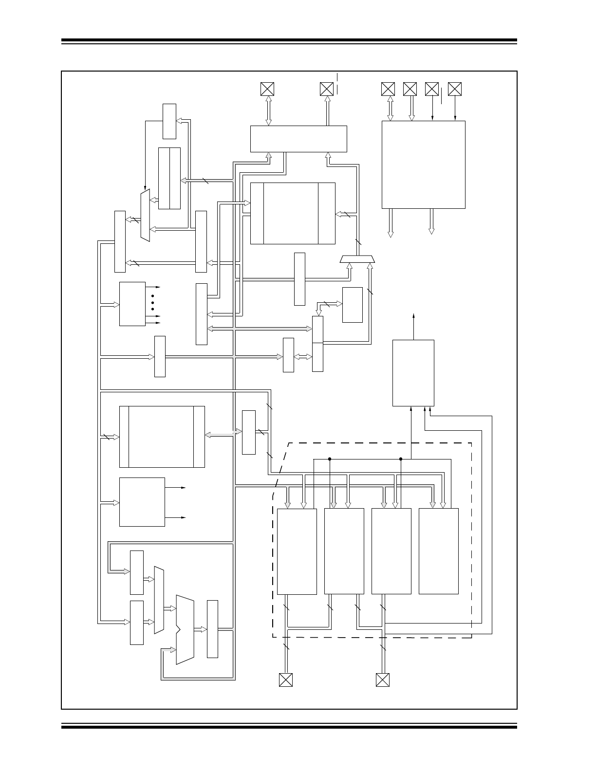
Simplified block diagrams are shown in Figure 3-1 and
Figure 3-2. The descriptions of the device pins are
listed in Table 3-1.
Hex Value
Signed Value
Math
Unsigned Value
Math
FFh
+ 01h
= ?
-127
+ 1
= -126 (FEh)
255
+ 1
= 0 (00h);
Carry bit = 1
This document was created with FrameMaker 4 0 4
PIC17C4X
DS30412C-page 10
1996 Microchip Technology Inc.
FIGURE 3-1:
PIC17C42 BLOCK DIAGRAM
CLOCK GENERA
T
O
R
PO
WER ON RESET
W
A
TCHDOG TIMER
OSC ST
AR
TUP
TIMER
TEST MODE SELECT
SYSTEM
D
A
T
A
LA
TCH
ADDRESS LA
TCH
PR
OGRAM
MEMOR
Y
(EPR
OM/R
OM)
T
ABLE PTR<16>
ST
A
C
K
16 x 16
PCH
PCL
PCLA
TH<8>
T
ABLE LA
TCH <16>
R
OM LA
TCH <16>
LITERAL
INSTR
UCTION
DECODER
CONTR
OL OUTPUTS
IR LA
TCH <16>
FSR0
FSR1
8
8
8
IR BUS <16>
RAM ADDR B
UFFER
D
A
T
A
LA
TCH
READ/WRITE
DECODE
FOR REGISTERS
MAPPED
IN D
A
T
A
SP
A
C
E
WREG <8>
BIT
OP
ALU
SHIFTER
IR BUS <16>
POR
TB
POR
T
A
RB0/CAP1
RB1/CAP2
RB2/PWM1
RB2/PWM2
RB4/TCLK12
RB5/TCLK3
RB6
RB7
RA0/INT
RA1/T0CKI
RA2
RA3
RA4/RX/DT
RA5/TX/CK
RA1/
Timer1, Timer2, Timer3
CAPTURE
PWM
DIGIT
AL I/O
POR
TS A, B
SERIAL POR
T
Timer0 MODULE
D
A
T
A
B
US <8>
IR BUS <7:0>
RA1/T0CKI
RA0/INT
86
8
6
2
6
4
3
IR <2:0>
DA
T A
BUS <8>
CONTR
OL
SIGNALS
T
O
CPU
CHIP_RESET
AND O
THER
CONTR
OL
SIGNALS
Q1, Q2, Q3, Q4
16
16
11
AD <15:0>
POR
TC and
ALE, WR
, OE
POR
TE
OSC1, OSC2
V
DD
, V
SS
MCLR
/V
PP
TEST
DECODE
BSR
INTERR
UPT
MODULE
8
RDF
WRF
T0CKI
PERIPHERALS
IR <7>
BU
S
INTER
-
FA
C
E
16
D
A
T
A
RAM
232x8
2K x 16
POR
TD