
2000 Microchip Technology Inc.
Preliminary
DS40197B-page 1
PIC16HV540
High-Performance RISC CPU:
• Only 33 single word instructions to learn
• All instructions are single cycle (200 ns) except for
program branches which are two-cycle
• Operating speed: DC - 20 MHz clock input
DC - 200 ns instruction cycle
• 12-bit wide instructions
• 8-bit wide data path
• Seven special function hardware registers
• Four-level deep hardware stack
• Direct, indirect and relative addressing modes for
data and instructions
Peripheral Features:
• 8-bit real time clock/counter (TMR0) with 8-bit pro-
grammable prescaler
• Power-On Reset (POR)
• Brown-Out Protection
• Device Reset Timer (DRT) with short RC oscilla-
tor start-up time
• Programmable Watchdog Timer (WDT) with its
own on-chip RC oscillator for reliable operation
• Sleep Timer
• 8 High Voltage I/O
• 4 Regulated I/O
• Wake up from SLEEP on-pin change
• Programmable code protection
• Power saving SLEEP mode
• Selectable oscillator options:
- RC:
Low-cost RC oscillator
- XT:
Standard crystal/resonator
- HS:
High speed crystal/resonator
- LP:
Power saving, low frequency crystal
• Glitch filtering on MCLR and pin change inputs
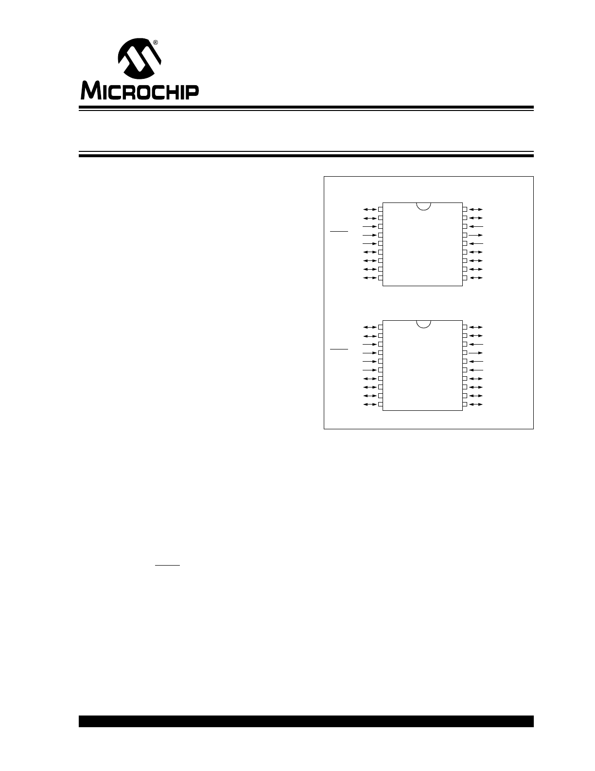
Pin Configurations
CMOS Technology:
• Selectable on-chip 3V/5V Regulator
• Low-power, high-speed CMOS EPROM technol-
ogy
• Fully static design
• Wide-operating voltage range:
- 3.5V to 15V
• Temperature range:
- Commercial: 0
°C to 70°C
- Industrial: -40
°C to 85°C
• Low-power consumption
- < 2 mA typical @ 5V, 4 MHz
- 15
µA typical @ 3V, 32 kHz
- < 4.5
µA typical standby current @ 15V (with
WDT disabled), 0
°C to 70°C
PDIP, SOIC, Windowed CERDIP
RA1
RA0
OSC1/CLKIN
OSC2/CLKOUT
V
DD
V
DD
RB7
RB6
RB5
RB4
RA2
RA3
T0CKI
MCLR/V
PP
V
SS
V
SS
RB0
RB1
RB2
RB3
•1
2
3
4
5
6
7
8
9
10
20
19
18
17
16
15
14
13
12
11
SSOP
P
IC16H
V540
RA1
RA0
OSC1/CLKIN
OSC2/CLKOUT
V
DD
RB7
RB6
RB5
RB4
RA2
RA3
T0CKI
MCLR/V
PP
V
SS
RB0
RB1
RB2
RB3
•1
2
3
4
5
6
7
8
9
18
17
16
15
14
13
12
11
PI
C16HV
540
10
Enhanced PIC16C54 EPROM-Based 8-Bit CMOS Microcontroller
With On-Chip Voltage Regulator

PIC16HV540
DS40197B-page 2
Preliminary
2000 Microchip Technology Inc.
Table of Contents
1.0
General Description ..................................................................................................................................... 3
2.0
PIC16HV540 Device Varieties ..................................................................................................................... 5
3.0
Architectural Overview ................................................................................................................................. 7
4.0
Memory Organization ................................................................................................................................ 11
5.0
I/O Ports..................................................................................................................................................... 19
6.0
Timer0 Module and TMR0 Register........................................................................................................... 25
7.0
Special Features of the CPU ..................................................................................................................... 31
8.0
Instruction Set Summary ........................................................................................................................... 43
9.0
Development Support ................................................................................................................................ 55
10.0
Electrical Characteristics - PIC16HV540 ................................................................................................... 61
11.0
DC and AC Characteristics - PIC16HV540................................................................................................ 69
12.0
Packaging Information ............................................................................................................................... 73
Index ........................................................................................................................................................................ 79
On-Line Support ....................................................................................................................................................... 81
Reader Response .................................................................................................................................................... 82
PIC16HV540 Product Identification System............................................................................................................. 83
To Our Valued Customers
Most Current Data Sheet
To obtain the most up-to-date version of this data sheet, please check our Worldwide Web site at:
http://www.microchip.com
You can determine the version of a data sheet by examining its literature number found on the bottom outside corner of any page.
The last character of the literature number is the version number. e.g., DS30000A is version A of document DS30000.
Errata
An errata sheet may exist for current devices, describing minor operational differences (from the data sheet) and recommended
workarounds. As device/documentation issues become known to us, we will publish an errata sheet. The errata will specify the revi-
sion of silicon and revision of document to which it applies.
To determine if an errata sheet exists for a particular device, please check with one of the following:
• Microchip’s Worldwide Web site; http://www.microchip.com
• Your local Microchip sales office (see last page)
• The Microchip Corporate Literature Center; U.S. FAX: (480) 786-7277
When contacting a sales office or the literature center, please specify which device, revision of silicon and data sheet (include liter-
ature number) you are using.
Corrections to this Data Sheet
We constantly strive to improve the quality of all our products and documentation. We have spent a great deal of time to ensure
that this document is correct. However, we realize that we may have missed a few things. If you find any information that is missing
or appears in error, please:
• Fill out and mail in the reader response form in the back of this data sheet.
• E-mail us at webmaster@microchip.com.
We appreciate your assistance in making this a better document.

2000 Microchip Technology Inc.
Preliminary
DS40197B-page 3
PIC16HV540
1.0
GENERAL DESCRIPTION
The PIC16HV540 from Microchip Technology is a low-
cost, high-performance, 8-bit, fully-static, EPROM-
based CMOS microcontroller. It is pin and software
compatible with the PIC16C5X family of devices. It
employs a RISC architecture with only 33 single word/
single cycle instructions. All instructions are single
cycle except for program branches, which take two
cycles. The PIC16HV540 delivers performance an
order of magnitude higher than its competitors in the
same price category. The 12-bit wide instructions are
highly orthogonal resulting in 2:1 code compression
over other 8-bit microcontrollers in its class. The easy-
to-use and easy-to-remember instruction set reduces
development time significantly.
The PIC16HV540 is the first One-Time-Programmable
(OTP) microcontroller with an on-chip 3 volt and 5 volt
regulator. This eliminates the need for an external reg-
ulator in many applications powered from 9 Volt or 12
Volt batteries or unregulated 6 volt, 9 volt or 12 volt
mains adapters. The PIC16HV540 is ideally suited for
applications that require very low standby current at
high voltages. These typically require expensive low
current regulators.
The PIC16HV540 is equipped with special features that
reduce system cost and power requirements. The Power-
On Reset (POR) and Device Reset Timer (DRT) eliminate
the need for external reset circuitry. There are four oscilla-
tor configurations to choose from, including the power-
saving LP (Low Power) oscillator, cost saving RC oscilla-
tor, and XT and HS for crystal oscillators. Power saving
SLEEP mode, Watchdog Timer and code protection fea-
tures improve system cost, power and reliability.
The UV erasable CERDIP packaged versions are ideal
for code development, while the cost-effective OTP ver-
sions are suitable for production in any volume. The
customer can take full advantage of Microchip’s price
leadership in OTP microcontrollers, while benefiting
from the OTP’s flexibility.
The PIC16HV540 is supported by a full-featured macro
assembler, a software simulator, an in-circuit emulator,
a low-cost development programmer, and a full fea-
tured programmer. All the tools are supported on IBM
PC and compatible machines.
1.1
Applications
The PIC16HV540 fits in low-power battery applications
such as CO and smoke detection, toys, games, secu-
rity systems and automobile modules. The EPROM
technology makes customizing of application programs
(transmitter codes, receiver frequencies, etc.)
extremely fast and convenient. The small footprint
package, for through hole or surface mounting, make
this microcontroller suitable for applications with space
limitations. Low-cost, low-power, high-performance,
ease of use and I/O flexibility make the PIC16HV540
very versatile even in areas where no microcontroller
use has been considered before (e.g., timer functions,
replacement of “glue” logic in larger systems, copro-
cessor applications).
1.2
Enhanced Features
1.2.1
REGULATED I/O PORTA INDEPENDENT
OF CORE REGULATOR
PORTA I/O pads and OSC2 output are powered by the
regulated internal voltage V
IO
. A maximum of 10mA per
output is allowed, or a total of 40mA. The core itself is
powered from the independently regulated supply
V
REG
.
1.2.2
HIGH VOLTAGE I/O PORTB
All eight PORTB I/Os are high voltage I/O. The inputs
will tolerate input voltages as high as the V
DD
and out-
puts will swing from V
SS
to the V
DD
. The input threshold
voltages vary with supply voltage. (See Electrical
Characteristics.)
1.2.3
WAKE-UP ON PIN CHANGE ON PORTB
[0:3]
Four of the PORTB inputs latch the status of the pin at
the onset of sleep mode. A level change on the inputs
resets the device, implementing wake up on pin change
(via warm reset). The PCWUF bit in the status register
is reset to indicate that a pin change caused the reset
condition. Any pin change (glitch insensitive) of the
opposite level of the initial value wakes up the device.
This option can be enabled/disabled in OPTION2 reg-
ister. (See OPTION2 Register, Register 4-3.)
1.2.4
WAKE-UP ON PIN CHANGE WITH A
SLOWLY-RISING VOLTAGE ON PORTB [7]
PORTB [7] also implements wake up from sleep, how-
ever this input is specifically adapted so that a slowly
rising voltage does not cause excessive power con-
sumption. This input can be used with external RC cir-
cuits for long sleep periods without using the internal
timer and prescaler. This option is also enabled/dis-
abled in OPTION2 register. (The enable/disable bit is
shared with the other 4 wake-up inputs.) The PCWUF
bit in the status register is also shared with the other
four wake-up inputs.
1.2.5
LOW-VOLTAGE (BROWN-OUT)
DETECTION
A low voltage (Brown-out) detect circuit optionally
resets the device at a voltage level higher than that at
which the PICmicro
®
device stops operating. The nom-
inal trip voltages are 3.1 volts (for 5 volt operation) and
2.2 volt (for 3 volt operation), respectively. The core
remains in the reset state as long as this condition
holds (as if a MCLR external reset was given). The
Brown-out trip level is user selectable, with built-in inter-
locks. The Brown-out detector is disabled at power-up
and is activated by clearing the appropriate bit
(BODEN) in OPTION2 register.
PIC16HV540
DS40197B-page 4
Preliminary
2000 Microchip Technology Inc.
1.2.6
INCREASED STACK DEPTH
The stack depth is 4 levels to allow modular program
implementation by using functions and subroutines.
1.2.7
ENHANCED WATCHDOG TIMER (WDT)
OPERATION
The WDT is enabled by setting FUSE 2 in the configuration
word. The WDT setting is latched and the fuse disabled
during SLEEP mode to reduce current consumption.
If the WDT is disabled by FUSE 2, it can be enabled/dis-
abled under program control using bit 4 in OPTION2 Reg-
ister (SWDTEN). The software WDT control is disabled at
power-up.
The current consumption of the on-chip oscillator (used
for the watchdog, oscillator startup timer and sleep
timer) is less than 1
µA (typical) at 3 Volt operation.
1.2.8
REDUCED EXTERNAL RC OSCILLATOR
STARTUP TIME
If the RC oscillator option is selected in the Configura-
tion word (FOSC1=1 and FOSCO=1), the oscillator
startup time is 1.0 ms nominal instead of 18 ms nomi-
nal. This is applicable after power-up (POR), either
WDT interrupt or wake-up, external reset on MCLR,
PCWU (wake on pin change) and Brown-out.
1.2.9
LOW-VOLTAGE OPERATION OF THE
ENTIRE CPU DURING SLEEP
The voltage regulator can automatically lower the volt-
age to the core from 5 Volt to 3 Volt during sleep, result-
ing in reduced current consumption. This is an option
bit (SL) in the OPTION2 register.
1.2.10
GLITCH FILTERS ON WAKE-UP PINS AND
MCLR
Glitch sensitive inputs for wake-up on pin change are
filtered to reduce susceptibility to interference. A similar
filter reduces false reset on MCLR.
1.2.11
PROGRAMMABLE CLOCK GENERATOR
When used in RC mode, the CLKOUT pin can be used
as a programmable clock output. The output is con-
nected to TMR0, bit 0 and by setting the prescaler,
clock out frequencies of CLKIN/8 to CLKIN/1024 can
be generated. The CLKOUT pin can also be used as a
general purpose output by modifying TMR0, bit 0.
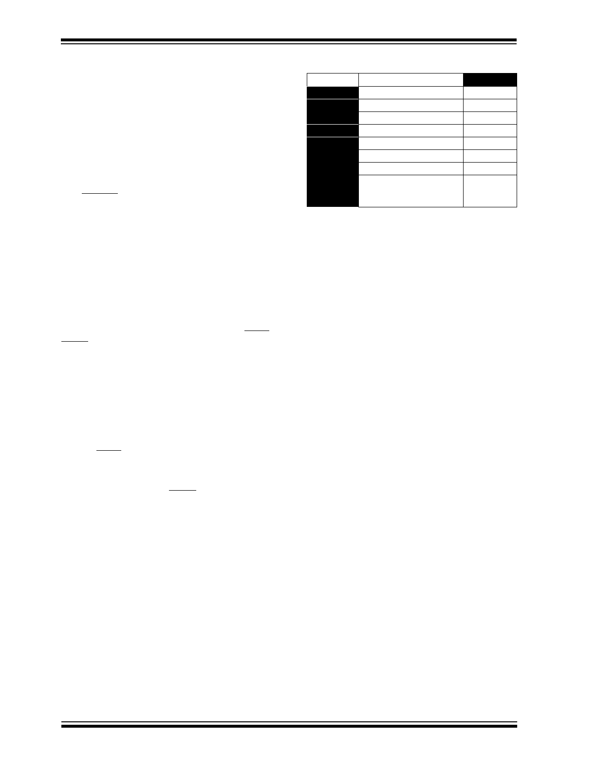
TABLE 1-1:
PIC16HV540 DEVICE
PIC16HV540
Clock
Maximum Frequency (MHz)
20
Memory
EPROM Program Memory
512
RAM Data Memory (bytes)
25
Peripherals
Timer Module(s)
TMR0
Packages
I/O Pins
12
Voltage Range (Volts)
3.5V-15V
Number of Instructions
33
Packages
18-pin DIP
SOIC
20-pin SSOP
All PICmicro
devices have Power-on Reset, selectable
WDT, selectable code protect and high I/O current capability.

2000 Microchip Technology Inc.
Preliminary
DS40197B-page 5
PIC16HV540
2.0
PIC16HV540 DEVICE
VARIETIES
A variety of frequency ranges and packaging options
are available. Depending on application and
production requirements, the proper device option can
be selected using the information in this section. When
placing orders, please use the PIC16HV540 Product
Identification System at the back of this data sheet to
specify the correct part number.
For the PIC16HV540 family of devices, there is one
device type, as indicated in the device number:
1.
HV, as in PIC16HV540. These devices have
EPROM program memory and operate over the
standard voltage range of 3.5 to 15 volts.
2.1
UV Erasable Devices
The UV erasable versions, offered in CERDIP pack-
ages, are optimal for prototype development and pilot
programs.
UV erasable devices can be programmed for any of the
four oscillator configurations. Microchip’s PICSTART
and PRO MATE
programmers both support program-
ming of the PIC16HV540. Third party programmers
also are available; refer to Literature Number DS00104
for a list of sources.
2.2
One-Time-Programmable (OTP)
Devices
The availability of OTP devices is especially useful for
customers expecting frequent code changes and
updates.
The OTP devices, packaged in plastic packages, per-
mit the user to program them once. In addition to the
program memory, the configuration bits must be pro-
grammed.
2.3
Quick-Turnaround-Production (QTP)
Devices
Microchip offers a QTP Programming Service for fac-
tory production orders. This service is made available
for users who choose not to program a medium to high
quantity of units and whose code patterns have stabi-
lized. The devices are identical to the OTP devices but
with all EPROM locations and configuration bit options
already programmed by the factory. Certain code and
prototype verification procedures apply before produc-
tion shipments are available. (Please contact your
Microchip Technology sales office for more details.)
2.4
Serialized Quick-Turnaround-
Production (SQTP) Devices
Microchip offers the unique programming service
where a few user-defined locations in each device are
programmed with different serial numbers. The serial
numbers may be random, pseudo-random or sequen-
tial.
Serial programming allows each device to have a
unique number which can serve as an entry code,
password or ID number. (Please contact your Microchip
Technology sales office for more details.)

PIC16HV540
DS40197B-page 6
Preliminary
2000 Microchip Technology Inc.
NOTES:

2000 Microchip Technology Inc.
Preliminary
DS40197B-page 7
PIC16HV540
3.0
ARCHITECTURAL OVERVIEW
The high performance of the PIC16HV540 can be
attributed to a number of architectural features com-
monly found in RISC microprocessors. To begin with,
the PIC16HV540 uses a Harvard architecture in which
program and data are accessed on separate buses.
This improves bandwidth over traditional von Neumann
architecture where program and data are fetched on
the same bus. Separating program and data memory
further allows instructions to be sized differently than
the 8-bit wide data word. Instruction opcodes are 12-
bits wide making it possible to have all single word
instructions. A 12-bit wide program memory access
bus fetches a 12-bit instruction in a single cycle. A two-
stage pipeline overlaps fetch and execution of instruc-
tions. Consequently, all instructions (33) execute in a
single cycle (200ns @ 20MHz) except for program
branches.
The PIC16HV540 address 512 x 12 of program mem-
ory. All program memory is internal.
The PIC16HV540 can directly or indirectly address its
register files and data memory. All special function reg-
isters including the program counter are mapped in the
data memory. The PIC16HV540 has a highly orthogo-
nal (symmetrical) instruction set that makes it possible
to carry out any operation on any register using any
addressing mode. This symmetrical nature and lack of
‘special optimal situations’ make programming with the
PIC16HV540 simple yet efficient. In addition, the learn-
ing curve is reduced significantly.
The PIC16HV540 device contains an 8-bit ALU and
working register. The ALU is a general purpose arith-
metic unit. It performs arithmetic and Boolean functions
between data in the working register and any register
file.
The ALU is 8-bits wide and capable of addition, sub-
traction, shift and logical operations. Unless otherwise
mentioned, arithmetic operations are two's comple-
ment in nature. In two-operand instructions, typically
one operand is the W (working) register. The other
operand is either a file register or an immediate con-
stant. In single operand instructions, the operand is
either the W register or a file register.
The W register is an 8-bit working register used for ALU
operations. It is not an addressable register.
Depending on the instruction executed, the ALU may
affect the values of the Carry (C), Digit Carry (DC),
and Zero (Z) bits in the STATUS register. The C and
DC bits operate as a borrow and digit borrow out bit,
respectively, in subtraction. See the SUBWF and ADDWF
instructions for examples.
A simplified block diagram is shown in Figure 3-1, with
the corresponding device pins described in Table 3-1.
PIC16HV540
DS40197B-page 8
Preliminary
2000 Microchip Technology Inc.
FIGURE 3-1:
PIC16HV540 BLOCK DIAGRAM
V
REG
3V/5V
Regulator
V
DD
BOD
PC
(PIN CHANGE)
FILTER
RB7
PCWU
4
RB<3:0>
RL/SL
BODL/BODEN
SWDTEN (OPTION2 REGISTER)
OSC1 OSC2 MCLR
CONFIGURATION WORD
EPROM
512 X 12
INSTRUCTION
REGISTER
INSTRUCTION
DECODER
PC
9-11
9-11
12
12
9
8
DIRECT ADDRESS
WDT
TIME
OUT
STACK 1
STACK 2
STACK 3
STACK 4
HIGH VOLTAGE
TRANSLATION
RL/SL
T0CKI
PIN
“DISABLE”
“OSC
SELECT”
2
WATCHDOG
TIMER
“CODE
PROTECT”
8
OSCILLATOR/
TIMING &
CONTROL
“SLEEP”
CLKOUT
WDT/TMR0
PRESCALER
6
6
“OPTION”
FROM W
FROM W
GENERAL
PURPOSE
REGISTER
FILE
(SRAM)
25 Bytes
“TRIS 7”
DIRECT RAM
ADDRESS
5
OPTION2
OPTION REG
5-7
8
FSR
TMR0
DATA BUS
8
8
8
8
8
4
4
4
FROM W
FROM W
“TRIS 6”
PORTB
PORTA
TRISB
TRISA
RB<7:0>
RA<3:0>
V
IO
3V/5V
Regulator
“TRIS 5”
ALU
STATUS
W
LIT
E
R
A
L
S
2000 Microchip Technology Inc.
Preliminary
DS40197B-page 9
PIC16HV540
TABLE 3-1:
PINOUT DESCRIPTION - PIC16HV540
Name
DIP, SOIC
No.
SSOP
No.
I/O/P
Type
Input
Levels
Description
RA0
RA1
RA2
RA3
17
18
1
2
19
20
1
2
I/O
I/O
I/O
I/O
TTL
TTL
TTL
TTL
Independently regulated Bi-directional I/O port — V
IO
RB0
RB1
RB2
RB3
6
7
8
9
7
8
9
10
I/O
I/O
I/O
I/O
TTL
TTL
TTL
TTL
High-voltage Bi-directional I/O port.
Sourced from V
DD
.
Wake-up on pin
change
RB4
RB5
RB6
10
11
12
11
12
13
I/O
I/O
I/O
TTL
TTL
TTL
RB7
13
14
I/O
TTL
Wake-up on SLOW
rising pin change.
T0CKI
3
3
I
ST
Clock input to Timer 0. Must be tied to V
SS
or V
DD,
if not in
use, to reduce current consumption.
MCLR/V
PP
4
4
I
ST
Master clear (reset) input/programming voltage input. This
pin is an active low reset to the device. Voltage on the MCLR/
V
PP
pin must not exceed V
DD
(1)
to avoid unintended entering
of programming mode.
OSC1/CLKIN
16
18
I
ST
Oscillator crystal input/external clock source input.
OSC2/CLKOUT
15
17
O
—
Oscillator crystal output. Connects to crystal or resonator in
crystal oscillator mode. In RC mode, OSC2/CLKOUT output
is connected to TMR0, bit 0. Frequencies of CLKIN/8 to
CLKIN/1024 can be generated on this pin.
V
DD
14
15,16
P
—
Positive supply.
V
SS
5
5,6
P
—
Ground reference.
Legend: I = input, O = output, I/O = input/output, P = power, — = Not Used, TTL = TTL input, ST = Schmitt Trigger input.
Note 1: V
DD
during programming mode can not exceed parameter PD1 called out in the PIC16C5X Programming
Specification (Literature number DS30190).
PIC16HV540
DS40197B-page 10
Preliminary
2000 Microchip Technology Inc.
3.1
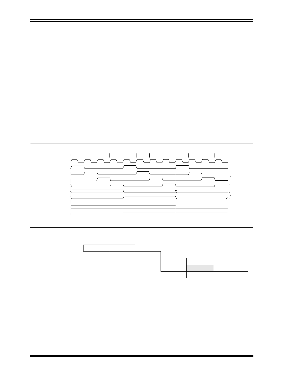
Clocking Scheme/Instruction Cycle
The clock input (OSC1/CLKIN pin) is internally divided
by four to generate four non-overlapping quadrature
clocks namely Q1, Q2, Q3 and Q4. Internally, the pro-
gram counter is incremented every Q1, and the instruc-
tion is fetched from program memory and latched into
instruction register in Q4. It is decoded and executed
during the following Q1 through Q4. The clocks and
instruction execution flow is shown in Figure 3-2 and
Example 3-1.
3.2
Instruction Flow/Pipelining
An Instruction Cycle consists of four Q cycles (Q1, Q2,
Q3 and Q4). The instruction fetch and execute are
pipelined such that fetch takes one instruction cycle
while decode and execute takes another instruction
cycle. However, due to the pipelining, each instruction
effectively executes in one cycle. If an instruction
causes the program counter to change (e.g., GOTO)
then two cycles are required to complete the instruction
(Example 3-1).
A fetch cycle begins with the program counter (PC)
incrementing in Q1.
In the execution cycle, the fetched instruction is latched
into the Instruction Register (IR) in cycle Q1. This
instruction is then decoded and executed during the
Q2, Q3, and Q4 cycles. Data memory is read during Q2
(operand read) and written during Q4 (destination
write).
FIGURE 3-2:
CLOCK/INSTRUCTION CYCLE
EXAMPLE 3-1:
INSTRUCTION PIPELINE FLOW
Q1
Q2
Q3
Q4
Q1
Q2
Q3
Q4
Q1
Q2
Q3
Q4
OSC1
Q1
Q2
Q3
Q4
PC
OSC2/CLKOUT
(RC mode)
PC
PC+1
PC+2
Fetch INST (PC)
Execute INST (PC-1)
Fetch INST (PC+1)
Execute INST (PC)
Fetch INST (PC+2)
Execute INST (PC+1)
Internal
phase
clock
Note 1: Frequencies of CLKIN8 to CLKIN/1024 are possible.
CLKIN/8
(1)
All instructions are single cycle, except for any program branches. These take two cycles since the fetch instruction is “flushed”
from the pipeline while the new instruction is being fetched and then executed.
1. MOVLW 55H
Fetch 1
Execute 1
2. MOVWF PORTB
Fetch 2
Execute 2
3. CALL SUB_1
Fetch 3
Execute 3
4. BSF PORTA, BIT3
Fetch 4
Flush
Fetch SUB_1 Execute SUB_1