
1997 Microchip Technology Inc.
DS30444E - page 1
PIC16C9XX
8-Bit CMOS Microcontroller with LCD Driver
Devices included in this data sheet:
• PIC16C923
• PIC16C924
Microcontroller Core Features:
• High performance RISC CPU
• Only 35 single word instructions to learn
• 4K x 14 on-chip EPROM program memory
• 176 x 8 general purpose registers (SRAM)
• All single cycle instructions (500 ns) except for
program branches which are two-cycle
• Operating speed: DC - 8 MHz clock input
DC - 500 ns instruction cycle
• Interrupt capability
• Eight level deep hardware stack
• Direct, indirect and relative addressing modes
Peripheral Features:
• 25 I/O pins with individual direction control
• 25-27 input only pins
• Timer0: 8-bit timer/counter with 8-bit prescaler
• Timer1: 16-bit timer/counter, can be incremented
during sleep via external crystal/clock
• Timer2: 8-bit timer/counter with 8-bit period regis-
ter, prescaler and postscaler
• One pin that can be configured a capture input,
PWM output, or compare output
- Capture is 16-bit, max. resolution 31.25 ns
- Compare is 16-bit, max. resolution 500 ns
- PWM max resolution is 10-bits.
Maximum PWM frequency @ 8-bit resolution
= 32 kHz, @ 10-bit resolution = 8 kHz
• Programmable LCD timing module
- Multiple LCD timing sources available
- Can drive LCD panel while in Sleep mode
- Static, 1/2, 1/3, 1/4 multiplex
- Static drive and 1/3 bias capability
- 16 bytes of dedicated LCD RAM
- Up to 32 segments, up to 4 commons
Common
Segment
Pixels
1
32
32
2
31
62
3
30
90
4
29
116
Available in Die Form
• Synchronous Serial Port (SSP) with SPI
and I
2
C
• 8-bit multi-channel Analog to Digital converter
(PIC16C924 only)
Special Microcontroller Features:
• Power-on Reset (POR)
• Power-up Timer (PWRT) and Oscillator Start-up
Timer (OST)
• Watchdog Timer (WDT) with its own on-chip RC
oscillator for reliable operation
• Programmable code-protection
• Power saving SLEEP mode
• Selectable oscillator options
• In-Circuit Serial Programming™ (via two pins)
CMOS Technology
• Low-power, high-speed CMOS EPROM
technology
• Fully static design
• Wide operating voltage range: 2.5V to 6.0V
• Commercial and Industrial temperature ranges
• Low-power consumption:
- < 2 mA @ 5.5V, 4 MHz
- 22.5
µ
A typical @ 4V, 32 kHz
- < 1
µ
A typical standby current @ 3.0V
ICSP is a trademark of Microchip Technology Inc. I
2
C is a trademark of Philips Corporation. SPI is a trademark of Motorola Corporation.
PIC16C9XX
DS30444E - page 2
1997 Microchip Technology Inc.
Pin Diagrams
TQFP
1
2
3
4
5
6
7
8
9
10
11
12
13
14
15
16
48
47
46
45
44
43
42
41
40
39
38
37
36
35
34
33
64
63
62
61
60
59
58
57
56
55
54
53
52
51
50
49
17
18
19
20
21
22
23
24
25
26
27
28
29
30
31
32
PIC16C923
RD5/SEG29/COM3
RG6/SEG26
RG3/SEG23
RG2/SEG22
RG1/SEG21
RG0/SEG20
RF7/SEG19
RF6/SEG18
RF5/SEG17
RF4/SEG16
RF3/SEG15
RF2/SEG14
RF1/SEG13
RF0/SEG12
RA4/T0CKI
RA5/SS
RB1
RB0/INT
RC3/SCK/SCL
RC4/SDI/SDA
RC5/SDO
V
LCD
2
V
LCD
3
V
DD
V
SS
C1
C2
OSC1/CLKIN
OSC2/CLKOUT
RC0/T1OSO/T1CKI
RA3
RA2
V
SS
RA1
RA0
RB2
RB3
RB4
RB5
RB7
RB6
V
DD
COM0
RD7/SEG31/COM1
RD6/SEG30/COM2
RC1/T1OSI
RC2/CCP1
V
LCD
1
VLCDADJ
RD0/SEG00
RD1/SEG01
RD2/SEG02
RD3/SEG03
RD4/SEG04
RE0/SEG05
RE1/SEG06
RE2/SEG07
RE3/SEG08
RE4/SEG09
RE6/SEG11
RE5/SEG10
RG5/SEG25
RG4/SEG24
MCLR
/V
PP
10
11
12
13
14
15
16
17
18
19
20
21
22
23
24
25
26
60
59
58
57
56
55
54
53
52
51
50
49
48
47
46
45
44
9
8
7
6
5
4
3
2
1
68
67
66
65
64
63
62
61
27
28
29
30
31
32
33
34
35
36
37
38
39
40
41
42
43
PIC16C923
RD5/SEG29/COM3
RG6/SEG26
RG5/SEG25
RG4/SEG24
RG3/SEG23
RG2/SEG22
RG1/SEG21
RG0/SEG20
RG7/SEG28
RF7/SEG19
RF6/SEG18
RF5/SEG17
RF4/SEG16
RF3/SEG15
RF2/SEG14
RF1/SEG13
RF0/SEG12
RA4/T0CKI
RA5/SS
RB1
RB0/INT
RC3/SCK/SCL
RC4/SDI/SDA
RC5/SDO
V
LCD
2
V
LCD
3
V
DD
V
DD
V
SS
C1
C2
OSC1/CLKIN
OSC2/CLKOUT
RC0/T1OSO/T1CKI
RA3
RA2
V
SS
RA1
RA0
RB2
RB3
MCLR
/V
PP
N/C
RB4
RB5
RB7
RB6
V
DD
COM0
RD7/SEG31/COM1
RD6/SEG30/COM2
RC1/T1OSI
RC2/CCP1
V
LCD
1
VLCDADJ
RD0/SEG00
RD1/SEG01
RD2/SEG02
RD3/SEG03
RD4/SEG04
RE7/SEG27
RE0/SEG05
RE1/SEG06
RE2/SEG07
RE3/SEG08
RE4/SEG09
RE6/SEG11
RE5/SEG10
PLCC
Input Pin
Output Pin
Digital Input/LCD Output Pin
LEGEND:
Input/Output Pin
LCD Output Pin
Shrink PDIP (750 mil)
RB4
RB5
RB7
RB6
V
DD
COM0
RD7/SEG31/COM1
RD6/SEG30/COM2
RD5/SEG29/COM3
RG6/SEG26
RG5/SEG25
RG4/SEG24
RG3/SEG23
RG2/SEG22
RG1/SEG21
RG0/SEG20
RF7/SEG19
RF6/SEG18
RF5/SEG17
RF4/SEG16
MCLR/V
PP
RB3
RB2
RA0
RA1
V
SS
RA2
RA4/T0CKI
RA5/SS
RB1
RB0/INT
RC3/SCK/SCL
RC4/SDI/SDA
RC5/SDO
V
LCD
2
V
LCD
3
V
DD
V
SS
C1
C2
1
2
3
4
5
6
7
8
9
10
11
12
13
14
15
16
17
18
19
20
64
63
62
61
60
59
58
57
56
55
54
53
52
51
50
49
48
47
46
45
PIC16C923
OSC1/CLKIN
OSC2/CLKOUT
RC0/T1OSO/T1CKI
RC1/T1OSI
RC2/CCP1
V
LCD
1
VLCDADJ
RD0/SEG00
RD1/SEG01
RD2/SEG02
RD3/SEG03
21
22
23
24
25
26
27
28
29
30
31
32
RA3
40
39
38
37
36
35
34
33
44
43
42
41
RF3/SEG15
RF2/SEG14
RF1/SEG13
RF0/SEG12
RE6/SEG11
RE5/SEG10
RE4/SEG09
RE3/SEG08
RE2/SEG07
RE1/SEG06
RE0/SEG05
RD4/SEG04
1997 Microchip Technology Inc.
DS30444E - page 3
PIC16C9XX
Pin Diagrams (Cont.’d)
10
11
12
13
14
15
16
17
18
19
20
21
22
23
24
25
26
60
59
58
57
56
55
54
53
52
51
50
49
48
47
46
45
44
9
8
7
6
5
4
3
2
1
68
67
66
65
64
63
62
61
27
28
29
30
31
32
33
34
35
36
37
38
39
40
41
42
43
PIC16C924
RD5/SEG29/COM3
RG6/SEG26
RG5/SEG25
RG4/SEG24
RG3/SEG23
RG2/SEG22
RG1/SEG21
RG0/SEG20
RG7/SEG28
RF7/SEG19
RF6/SEG18
RF5/SEG17
RF4/SEG16
RF3/SEG15
RF2/SEG14
RF1/SEG13
RF0/SEG12
RA4/T0CKI
RA5/AN4/SS
RB1
RB0/INT
RC3/SCK/SCL
RC4/SDI/SDA
RC5/SDO
V
LCD
2
V
LCD
3
A
VDD
V
DD
V
SS
C1
C2
OSC1/CLKIN
OSC2/CLKOUT
RC0/T1OSO/T1CKI
RA3/AN3/V
REF
RA2/AN2
V
SS
RA1/AN1
RA0/AN0
RB2
RB3
MCLR
/V
PP
N/C
RB4
RB5
RB7
RB6
V
DD
COM0
RD7/SEG31/COM1
RD6/SEG30/COM2
RC1/T1OSI
RC2/CCP1
V
LCD
1
VLCDADJ
RD0/SEG00
RD1/SEG01
RD2/SEG02
RD3/SEG03
RD4/SEG04
RE7/SEG27
RE0/SEG05
RE1/SEG06
RE2/SEG07
RE3/SEG08
RE4/SEG09
RE6/SEG11
RE5/SEG10
PLCC
TQFP
1
2
3
4
5
6
7
8
9
10
11
12
13
14
15
16
48
47
46
45
44
43
42
41
40
39
38
37
36
35
34
33
64
63
62
61
60
59
58
57
56
55
54
53
52
51
50
49
17
18
19
20
21
22
23
24
25
26
27
28
29
30
31
32
PIC16C924
RD5/SEG29/COM3
RG6/SEG26
RG3/SEG23
RG2/SEG22
RG1/SEG21
RG0/SEG20
RF7/SEG19
RF6/SEG18
RF5/SEG17
RF4/SEG16
RF3/SEG15
RF2/SEG14
RF1/SEG13
RF0/SEG12
RA4/T0CKI
RA5/AN4/SS
RB1
RB0/INT
RC3/SCK/SCL
RC4/SDI/SDA
RC5/SDO
V
LCD
2
V
LCD
3
V
DD
V
SS
C1
C2
OSC1/CLKIN
OSC2/CLKOUT
RC0/T1OSO/T1CKI
RA3/AN3/
V
REF
RA2/AN2
V
SS
RA1/AN1
RA0/AN0
RB2
RB3
RB4
RB5
RB7
RB6
V
DD
COM0
RD7/SEG31/COM1
RD6/SEG30/COM2
RC1/T1OSI
RC2/CCP1
V
LCD
1
VLCDADJ
RD0/SEG00
RD1/SEG01
RD2/SEG02
RD3/SEG03
RD4/SEG04
RE0/SEG05
RE1/SEG06
RE2/SEG07
RE3/SEG08
RE4/SEG09
RE6/SEG11
RE5/SEG10
RG5/SEG25
RG4/SEG24
MCLR
/V
PP
Input Pin
Output Pin
Digital Input/LCD Output Pin
LEGEND:
Input/Output Pin
LCD Output Pin
Shrink PDIP (750 mil)
RB4
RB5
RB7
RB6
V
DD
COM0
RD7/SEG31/COM1
RD6/SEG30/COM2
RD5/SEG29/COM3
RG6/SEG26
RG5/SEG25
RG4/SEG24
RG3/SEG23
RG2/SEG22
RG1/SEG21
RG0/SEG20
RF7/SEG19
RF6/SEG18
RF5/SEG17
RF4/SEG16
MCLR/V
PP
RB3
RB2
RA0/AN0
RA1/AN1
V
SS
RA2/AN2
RA4/T0CKI
RA5/AN4/SS
RB1
RB0/INT
RC3/SCK/SCL
RC4/SDI/SDA
RC5/SDO
V
LCD
2
V
LCD
3
V
DD
V
SS
C1
C2
1
2
3
4
5
6
7
8
9
10
11
12
13
14
15
16
17
18
19
20
64
63
62
61
60
59
58
57
56
55
54
53
52
51
50
49
48
47
46
45
PIC16C924
OSC1/CLKIN
OSC2/CLKOUT
RC0/T1OSO/T1CKI
RC1/T1OSI
RC2/CCP1
V
LCD
1
VLCDADJ
RD0/SEG00
RD1/SEG01
RD2/SEG02
RD3/SEG03
21
22
23
24
25
26
27
28
29
30
31
32
RA3/AN3/V
REF
40
39
38
37
36
35
34
33
44
43
42
41
RF3/SEG15
RF2/SEG14
RF1/SEG13
RF0/SEG12
RE6/SEG11
RE5/SEG10
RE4/SEG09
RE3/SEG08
RE2/SEG07
RE1/SEG06
RE0/SEG05
RD4/SEG04

PIC16C9XX
DS30444E - page 4
1997 Microchip Technology Inc.
Table of Contents
1.0
General Description..................................................................................................................................................................... 5
2.0
PIC16C9XX Device Varieties ...................................................................................................................................................... 7
3.0
Architectural Overview ................................................................................................................................................................ 9
4.0
Memory Organization ................................................................................................................................................................ 17
5.0
Ports .......................................................................................................................................................................................... 31
6.0
Overview of Timer Modules....................................................................................................................................................... 43
7.0
Timer0 Module .......................................................................................................................................................................... 45
8.0
Timer1 Module .......................................................................................................................................................................... 51
9.0
Timer2 Module .......................................................................................................................................................................... 55
10.0
Capture/Compare/PWM (CCP) Module .................................................................................................................................... 57
11.0
Synchronous Serial Port (SSP) Module .................................................................................................................................... 63
12.0
Analog-to-Digital Converter (A/D) Module ................................................................................................................................. 79
13.0
LCD Module .............................................................................................................................................................................. 89
14.0
Special Features of the CPU ................................................................................................................................................... 103
15.0
Instruction Set Summary ......................................................................................................................................................... 119
16.0
Development Support.............................................................................................................................................................. 137
17.0
Electrical Characteristics ......................................................................................................................................................... 141
18.0
DC and AC Characteristics Graphs and Tables ...................................................................................................................... 161
19.0
Packaging Information............................................................................................................................................................. 171
Appendix A:
................................................................................................................................................................................... 175
Appendix B:
Compatibility ............................................................................................................................................................. 175
Appendix C:
What’s New................................................................................................................................................................ 176
Appendix D:
What’s Changed ........................................................................................................................................................ 176
Index .................................................................................................................................................................................................. 177
List of Equations And Examples ........................................................................................................................................................ 181
List of Figures..................................................................................................................................................................................... 181
List of Tables...................................................................................................................................................................................... 182
Reader Response .............................................................................................................................................................................. 186
PIC16C9XX Product Identification System ........................................................................................................................................ 187
To Our Valued Customers
We constantly strive to improve the quality of all our products and documentation. We have spent an exceptional
amount of time to ensure that these documents are correct. However, we realize that we may have missed a few
things. If you find any information that is missing or appears in error, please use the reader response form in the
back of this data sheet to inform us. We appreciate your assistance in making this a better document.

1997 Microchip Technology Inc.
DS30444E- page 5
PIC16C9XX
1.0
GENERAL DESCRIPTION
The PIC16C9XX is a family of
low-cost, high-perfor-
mance, CMOS, fully-static, 8-bit microcontrollers with
an integrated LCD Driver module, in the PIC16CXXX
mid-range family.
All PICmicro™ microcontrollers employ an advanced
RISC architecture. The PIC16CXXX microcontroller
family has enhanced core features, eight-level deep
stack, and multiple internal and external interrupt
sources.
The separate instruction and data buses of the
Harvard architecture allow a 14-bit wide instruction
word with the separate 8-bit wide data. The two stage
instruction pipeline allows all instructions to execute in
a single cycle, except for program branches (which
require two cycles). A total of 35 instructions (reduced
instruction set) are available. Additionally, a large regis-
ter set gives some of the architectural innovations used
to achieve a very high performance.
PIC16CXXX microcontrollers typically achieve a 2:1
code compression and a 4:1 speed improvement over
other 8-bit microcontrollers in their class.
The
PIC16C923
devices have 176 bytes of RAM and
25 I/O pins. In addition several peripheral features are
available including: three timer/counters, one Cap-
ture/Compare/PWM module, one serial port and one
LCD module. The Synchronous Serial Port can be con-
figured as either a 3-wire Serial Peripheral Interface
(SPI) or the two-wire Inter-Integrated Circuit (I
2
C) bus.
The LCD module features programmable multiplex
mode (static, 1/2, 1/3 and 1/4) and drive bias (static and
1/3). It is capable of driving up to 32 segments and up
to 4 commons. It can also drive the LCD panel while in
SLEEP mode.
The
PIC16C924
devices have 176 bytes of RAM and
25 I/O pins. In addition several peripheral features are
available including: three timer/counters, one Cap-
ture/Compare/PWM module, one serial port and one
LCD module. The Synchronous Serial Port can be con-
figured as either a 3-wire Serial Peripheral Interface
(SPI) or the two-wire Inter-Integrated Circuit (I
2
C) bus.
The LCD module features programmable multiplex
mode (static, 1/2, 1/3 and 1/4) and drive bias (static and
1/3). It is capable of driving up to 32 segments and up
to 4 commons. It can also drive the LCD panel while in
SLEEP mode. The PIC16C924 also has an 5-channel
high-speed 8-bit A/D. The 8-bit resolution is ideally
suited for applications requiring low-cost analog inter-
face, e.g. thermostat control, pressure sensing, and
meters.
The PIC16C9XX family has special features to reduce
external components, thus reducing cost, enhancing
system reliability and reducing power consumption.
There are four oscillator options, of which the single pin
RC oscillator provides a low-cost solution, the LP oscil-
lator minimizes power consumption, XT is a standard
crystal, and the HS is for High Speed crystals. The
SLEEP (power-down) feature provides a power saving
mode. The user can wake up the chip from SLEEP
through several external and internal interrupts and
reset(s).
A highly reliable Watchdog Timer with its own on-chip
RC oscillator provides recovery in the event of a soft-
ware lock-up.
A UV erasable CERQUAD (compatible with PLCC)
packaged version is ideal for code development while
the cost-effective One-Time-Programmable (OTP) ver-
sion is suitable for production in any volume.
The PIC16C9XX family fits perfectly in applications
ranging from handheld meters, thermostats, to home
security products. The EPROM technology makes cus-
tomization of application programs (LCD panels, cali-
bration constants, sensor interfaces, etc.) extremely
fast and convenient. The small footprint packages make
this microcontroller series perfect for all applications
with space limitations. Low cost, low power, high perfor-
mance, ease of use and I/O flexibility make the
PIC16C9XX very versatile even in areas where no
microcontroller use has been considered before (e.g.
timer functions, capture and compare, PWM functions
and coprocessor applications).
1.1
Family and Upward Compatibility
Users familiar with the PIC16C5X microcontroller family
will realize that this is an enhanced version of the
PIC16C5X architecture. Please refer to Appendix A for
a detailed list of enhancements. Code written for the
PIC16C5X can be easily ported to the PIC16CXXX
family of devices (Appendix B).
1.2
Development Support
PIC16C9XX devices are supported by the complete
line of Microchip Development tools.
Please refer to Section 16.0 for more details about
Microchip’s development tools.
PIC16C9XX
DS30444E - page 6
1997 Microchip Technology Inc.
TABLE 1-1: PIC16C9XX FAMILY OF DEVICES
PIC16C923
PIC16C924
Clock
Maximum Frequency of Operation (MHz)
8
8
Memory
EPROM Program Memory
4K
4K
Data Memory (bytes)
176
176
Peripherals
Timer Module(s)
TMR0,
TMR1,
TMR2
TMR0,
TMR1,
TMR2
Capture/Compare/PWM Module(s)
1
1
Serial Port(s)
(SPI/I
2
C, USART)
SPI/I
2
C
SPI/I
2
C
Parallel Slave Port
—
—
A/D Converter (8-bit) Channels
—
5
LCD Module
4 Com,
32 Seg
4 Com,
32 Seg
Features
Interrupt Sources
8
9
I/O Pins
25
25
Input Pins
27
27
Voltage Range (Volts)
2.5-6.0
2.5-6.0
In-Circuit Serial Programming
Yes
Yes
Brown-out Reset
—
—
Packages
64-pin SDIP,
TQFP;
68-pin PLCC,
Die
64-pin SDIP,
TQFP;
68-pin PLCC,
Die
All PICmicro Family devices have Power-on Reset, selectable Watchdog Timer, selectable code protect and high I/O current capabil-
ity. All PIC16C9XX Family devices use serial programming with clock pin RB6 and data pin RB7.

1997 Microchip Technology Inc.
DS30444E - page 7
PIC16C9XX
2.0
PIC16C9XX DEVICE VARIETIES
A variety of frequency ranges and packaging options
are available. Depending on application and production
requirements, the proper device option can be selected
using the information in the PIC16C9XX Product Iden-
tification System section at the end of this data sheet.
When placing orders, please use that page of the data
sheet to specify the correct part number.
For the PIC16C9XX family, there are two device “types”
as indicated in the device number:
1.
C
, as in PIC16
C
924. These devices have
EPROM type memory and operate over the
standard voltage range.
2.
LC
, as in PIC16
LC
924. These devices have
EPROM type memory and operate over an
extended voltage range.
2.1
UV Erasable Devices
The UV erasable version, offered in CERQUAD pack-
age, is optimal for prototype development and pilot pro-
grams.
The UV erasable version can be erased and repro-
grammed to any of the configuration modes.
Microchip's
PICSTART
Plus and PRO MATE
II pro-
grammers both support the PIC16C9XX. Third party
programmers also are available; refer to the
Microchip
Third Party Guide
for a list of sources.
2.2
One-Time-Programmable (OTP)
Devices
The availability of OTP devices is especially useful for
customers who need the flexibility for frequent code
updates and small volume applications.
The OTP devices, packaged in plastic packages, permit
the user to program them once. In addition to the pro-
gram memory, the configuration bits must also be pro-
grammed.
2.3
Quick-Turnaround-Production (QTP)
Devices
Microchip offers a QTP Programming Service for fac-
tory production orders. This service is made available
for users who choose not to program a medium to high
quantity of units and whose code patterns have stabi-
lized. The devices are identical to the OTP devices but
with all EPROM locations and configuration options
already programmed by the factory. Certain code and
prototype verification procedures apply before produc-
tion shipments are available. Please contact your local
Microchip Technology sales office for more details.
2.4
Serialized Quick-Turnaround
Production (SQTP
SM
) Devices
Microchip offers a unique programming service where
a few user-defined locations in each device are pro-
grammed with different serial numbers. The serial num-
bers may be random, pseudo-random or sequential.
Serial programming allows each device to have a
unique number which can serve as an entry-code,
password or ID number.

PIC16C9XX
DS30444E - page 8
1997 Microchip Technology Inc.
NOTES:

1997 Microchip Technology Inc.
DS30444E - page 9
PIC16C9XX
3.0
ARCHITECTURAL OVERVIEW
The high performance of the PIC16CXXX family can be
attributed to a number of architectural features com-
monly found in RISC microprocessors. To begin with,
the PIC16CXXX uses a Harvard architecture, in which,
program and data are accessed from separate memo-
ries using separate buses. This improves bandwidth
over traditional von Neumann architecture where pro-
gram and data are fetched from the same memory
using the same bus. Separating program and data
buses further allows instructions to be sized differently
than the 8-bit wide data word. Instruction opcodes are
14-bits wide making it possible to have all single word
instructions. A 14-bit wide program memory access bus
fetches a 14-bit instruction in a single cycle. A
two-stage pipeline overlaps fetch and execution of
instructions (Example 3-1). Consequently, all instruc-
tions execute in a single cycle (500 ns @ 8 MHz) except
for program branches.
The PIC16C923 and PIC16C924 both address 4K x 14
of program memory and 176 x 8 of data memory.
The PIC16CXXX can directly or indirectly address its
register files or data memory. All special function regis-
ters, including the program counter, are mapped in the
data memory. The PIC16CXXX has an orthogonal
(symmetrical) instruction set that makes it possible to
carry out any operation on any register using any
addressing mode. This symmetrical nature and lack of
‘special optimal situations’ make programming with the
PIC16CXXX simple yet efficient, thus significantly
reducing the learning curve.
PIC16CXXX devices contain an 8-bit ALU and working
register. The ALU is a general purpose arithmetic unit.
It performs arithmetic and Boolean functions between
the data in the working register and any register file.
The ALU is 8-bits wide and capable of addition, sub-
traction, shift and logical operations. Unless otherwise
mentioned, arithmetic operations are two's comple-
ment in nature. In two-operand instructions, typically
one operand is the working register (W register). The
other operand is a file register or an immediate con-
stant. In single operand instructions, the operand is
either the W register or a file register.
The W register is an 8-bit working register used for ALU
operations. It is not an addressable register.
Depending on the instruction executed, the ALU may
affect the values of the Carry (C), Digit Carry (DC), and
Zero (Z) bits in the STATUS register. The C and DC bits
operate as a borrow bit and a digit borrow out bit,
respectively, in subtraction. See the
SUBLW
and
SUBWF
instructions for examples.
PIC16C9XX
DS30444E - page 10
1997 Microchip Technology Inc.
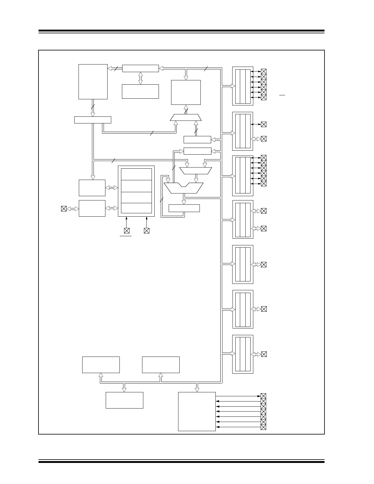
FIGURE 3-1:
PIC16C923 BLOCK DIAGRAM
EPROM
Program
Memory
4K x 14
13
Data Bus
8
14
Program
Bus
Instruction reg
Program Counter
8 Level Stack
(13-bit)
RAM
File
Registers
176 x 8
Direct Addr
7
RAM Addr
9
Addr MUX
Indirect
Addr
FSR reg
STATUS reg
MUX
ALU
W reg
Power-up
Timer
Oscillator
Start-up Timer
Power-on
Reset
Watchdog
Timer
Instruction
Decode &
Control
Timing
Generation
OSC1/CLKIN
OSC2/CLKOUT
MCLR
PORTA
PORTB
PORTC
PORTD
PORTE
RA4/T0CKI
RA5/SS
RB0/INT
RB1-RB7
RC0/T1OSO/T1CKI
RC1/T1OSI
RC2/CCP1
RC3/SCK/SCL
RC4/SDI/SDA
RC5/SDO
RD0-RD4/SEGnn
RE0-RE7/SEGnn
8
8
LCD
Synchronous
Timer0
Timer1, Timer2,
RA3
RA2
RA1
RA0
CCP1
Serial Port
V
LCD
1
PORTF
PORTG
RF0-RF7/SEGnn
RG0-RG7/SEGnn
RD5-RD7/SEGnn/COMn
COM0
3
8
V
DD
, V
SS
V
LCD
2
V
LCD
3
C1
C2
VLCDADJ