
1997 Microchip Technology Inc.
DS30272A-page 1
PIC16C71X
8-Bit CMOS Microcontrollers with A/D Converter
Devices included in this data sheet:
• PIC16C710
• PIC16C71
• PIC16C711
• PIC16C715
PIC16C71X Microcontroller Core Features:
• High-performance RISC CPU
• Only 35 single word instructions to learn
• All single cycle instructions except for program
branches which are two cycle
• Operating speed: DC - 20 MHz clock input
DC - 200 ns instruction cycle
• Up to 2K x 14 words of Program Memory,
up to 128 x 8 bytes of Data Memory (RAM)
• Interrupt capability
• Eight level deep hardware stack
• Direct, indirect, and relative addressing modes
• Power-on Reset (POR)
• Power-up Timer (PWRT) and
Oscillator Start-up Timer (OST)
• Watchdog Timer (WDT) with its own on-chip RC
oscillator for reliable operation
• Programmable code-protection
• Power saving SLEEP mode
• Selectable oscillator options
• Low-power, high-speed CMOS EPROM
technology
• Fully static design
• Wide operating voltage range: 2.5V to 6.0V
• High Sink/Source Current 25/25 mA
• Commercial, Industrial and Extended temperature
ranges
• Program Memory Parity Error Checking Circuitry
with Parity Error Reset (PER) (PIC16C715)
• Low-power consumption:
- < 2 mA @ 5V, 4 MHz
- 15
µ
A typical @ 3V, 32 kHz
- < 1
µ
A typical standby current
PIC16C71X Peripheral Features:
• Timer0: 8-bit timer/counter with 8-bit prescaler
• 8-bit multichannel analog-to-digital converter
• Brown-out detection circuitry for
Brown-out Reset (BOR)
• 13 I/O Pins with Individual Direction Control
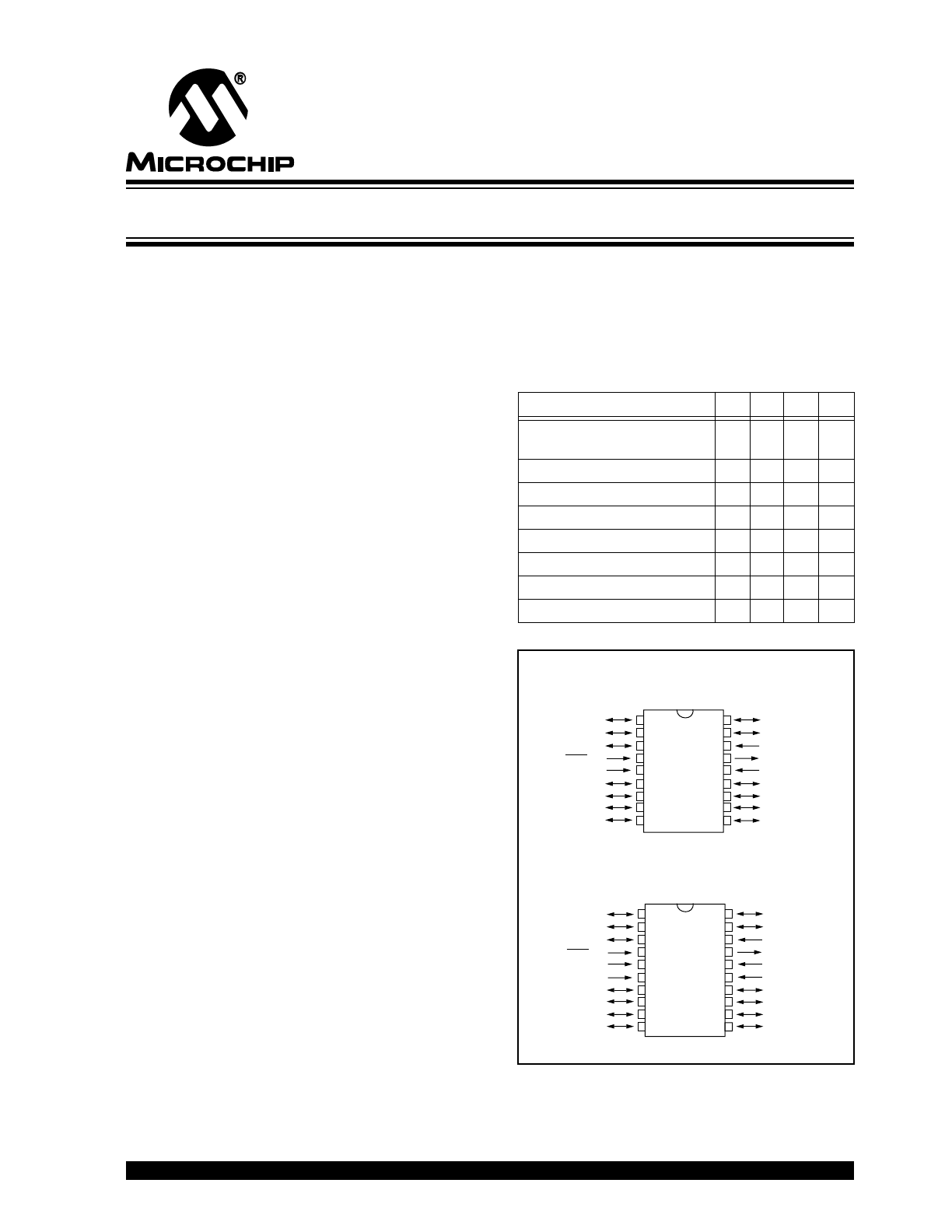
Pin Diagrams
PIC16C7X Features
710
71
711 715
Program Memory (EPROM)
x 14
512
1K
1K
2K
Data Memory (Bytes) x 8
36
36
68
128
I/O Pins
13
13
13
13
Timer Modules
1
1
1
1
A/D Channels
4
4
4
4
In-Circuit Serial Programming
Yes Yes Yes Yes
Brown-out Reset
Yes
—
Yes Yes
Interrupt Sources
4
4
4
4
RA2/AN2
RA3/AN3/V
REF
RA4/T0CKI
MCLR/V
PP
V
SS
V
SS
RB0/INT
RB1
RB2
RB3
RA1/AN1
RA0/AN0
OSC1/CLKIN
OSC2/CLKOUT
V
DD
RB7
RB6
RB5
RB4
• 1
2
3
4
5
6
7
8
9
10
20
19
18
17
16
15
14
13
12
11
V
DD
SSOP
RA2/AN2
RA3/AN3/V
REF
RA4/T0CKI
MCLR/V
PP
V
SS
RB0/INT
RB1
RB2
RB3
RA1/AN1
RA0/AN0
OSC1/CLKIN
OSC2/CLKOUT
V
DD
RB7
RB6
RB5
RB4
• 1
2
3
4
5
6
7
8
9
18
17
16
15
14
13
12
11
10
PIC16C710
PDIP, SOIC, Windowed CERDIP
PIC16C71
PIC16C711
PIC16C715
PIC16C710
PIC16C711
PIC16C715

PIC16C71X
DS30272A-page 2
1997 Microchip Technology Inc.
Table of Contents
1.0
General Description .................................................................................................................................................................... 3
2.0
PIC16C71X Device Varieties...................................................................................................................................................... 5
3.0
Architectural Overview................................................................................................................................................................ 7
4.0
Memory Organization ............................................................................................................................................................... 11
5.0
I/O Ports.................................................................................................................................................................................... 25
6.0
Timer0 Module.......................................................................................................................................................................... 31
7.0
Analog-to-Digital Converter (A/D) Module ................................................................................................................................ 37
8.0
Special Features of the CPU .................................................................................................................................................... 47
9.0
Instruction Set Summary .......................................................................................................................................................... 69
10.0
Development Support ............................................................................................................................................................... 85
11.0
Electrical Characteristics for PIC16C710 and PIC16C711 ....................................................................................................... 89
12.0
DC and AC Characteristics Graphs and Tables for PIC16C710 and PIC16C711.................................................................. 101
13.0
Electrical Characteristics for PIC16C715................................................................................................................................ 111
14.0
DC and AC Characteristics Graphs and Tables for PIC16C715 ............................................................................................ 125
15.0
Electrical Characteristics for PIC16C71.................................................................................................................................. 135
16.0
DC and AC Characteristics Graphs and Tables for PIC16C71 .............................................................................................. 147
17.0
Packaging Information ............................................................................................................................................................ 155
Appendix A: ...................................................................................................................................................................................... 161
Appendix B: Compatibility................................................................................................................................................................. 161
Appendix C: What’s New .................................................................................................................................................................. 162
Appendix D: What’s Changed .......................................................................................................................................................... 162
Index .................................................................................................................................................................................................. 163
PIC16C71X Product Identification System......................................................................................................................................... 173
To Our Valued Customers
We constantly strive to improve the quality of all our products and documentation. We have spent an exceptional
amount of time to ensure that these documents are correct. However, we realize that we may have missed a few
things. If you find any information that is missing or appears in error, please use the reader response form in the
back of this data sheet to inform us. We appreciate your assistance in making this a better document.

1997 Microchip Technology Inc.
DS30272A-page 3
PIC16C71X
1.0
GENERAL DESCRIPTION
The PIC16C71X is a family of
low-cost, high-perfor-
mance, CMOS, fully-static, 8-bit microcontrollers with
integrated analog-to-digital (A/D) converters, in the
PIC16CXX mid-range family.
All PIC16/17 microcontrollers employ an advanced
RISC architecture. The PIC16CXX microcontroller fam-
ily has enhanced core features, eight-level deep stack,
and multiple internal and external interrupt sources.
The separate instruction and data buses of the Harvard
architecture allow a 14-bit wide instruction word with
the separate 8-bit wide data. The two stage instruction
pipeline allows all instructions to execute in a single
cycle, except for program branches which require two
cycles. A total of 35 instructions (reduced instruction
set) are available. Additionally, a large register set gives
some of the architectural innovations used to achieve a
very high performance.
PIC16CXX microcontrollers typically achieve a 2:1
code compression and a 4:1 speed improvement over
other 8-bit microcontrollers in their class.
The
PIC16C710/71
devices have 36 bytes of RAM, the
PIC16C711
has 68 bytes of RAM and the
PIC16C715
has 128 bytes of RAM. Each device has 13 I/O
pins. In
addition a timer/counter is available. Also a 4-channel
high-speed 8-bit A/D is provided. The 8-bit resolution is
ideally suited for applications requiring low-cost analog
interface, e.g. thermostat control, pressure sensing,
etc.
The PIC16C71X family has special features to reduce
external components, thus reducing cost, enhancing
system reliability and reducing power consumption.
There are four oscillator options, of which the single pin
RC oscillator provides a low-cost solution, the LP oscil-
lator minimizes power consumption, XT is a standard
crystal, and the HS is for High Speed crystals. The
SLEEP (power-down) feature provides a power saving
mode. The user can wake up the chip from SLEEP
through several external and internal interrupts and
resets.
A highly reliable Watchdog Timer with its own on-chip
RC oscillator provides protection against software lock-
up.
A UV erasable CERDIP packaged version is ideal for
code development while the cost-effective One-Time-
Programmable (OTP) version is suitable for production
in any volume.
The PIC16C71X family fits perfectly in applications
ranging from security and remote sensors to appliance
control and automotive. The EPROM technology
makes customization of application programs (trans-
mitter codes, motor speeds, receiver frequencies, etc.)
extremely fast and convenient. The small footprint
packages make this microcontroller series perfect for
all applications with space limitations. Low cost, low
power, high performance, ease of use and I/O flexibility
make the PIC16C71X very versatile even in areas
where no microcontroller use has been considered
before (e.g. timer functions, serial communication, cap-
ture and compare, PWM functions and coprocessor
applications).
1.1
Family and Upward Compatibility
Users familiar with the PIC16C5X microcontroller fam-
ily will realize that this is an enhanced version of the
PIC16C5X architecture. Please refer to Appendix A for
a detailed list of enhancements. Code written for the
PIC16C5X can be easily ported to the PIC16CXX fam-
ily of devices (Appendix B).
1.2
Development Support
PIC16C71X devices are supported by the complete
line of Microchip Development tools.
Please refer to Section 10.0 for more details about
Microchip’s development tools.
PIC16C71X
DS30272A-page 4
1997 Microchip Technology Inc.
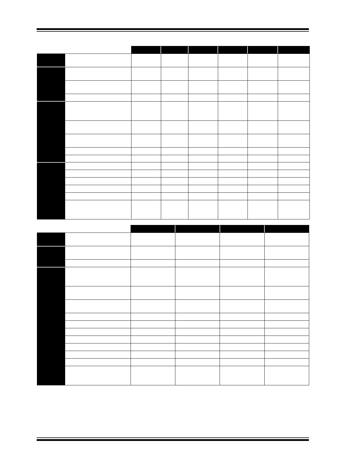
TABLE 1-1:
PIC16C71X FAMILY OF DEVICES
PIC16C710
PIC16C71
PIC16C711
PIC16C715
PIC16C72
PIC16CR72
(1)
Clock
Maximum Frequency
of Operation (MHz)
20
20
20
20
20
20
Memory
EPROM Program Memory
(x14 words)
512
1K
1K
2K
2K
—
ROM Program Memory
(14K words)
—
—
—
—
—
2K
Data Memory (bytes)
36
36
68
128
128
128
Peripherals
Timer Module(s)
TMR0
TMR0
TMR0
TMR0
TMR0,
TMR1,
TMR2
TMR0,
TMR1,
TMR2
Capture/Compare/PWM
Module(s)
—
—
—
—
1
1
Serial Port(s)
(SPI/I
2
C, USART)
—
—
—
—
SPI/I
2
C
SPI/I
2
C
Parallel Slave Port
—
—
—
—
—
—
A/D Converter (8-bit) Channels 4
4
4
4
5
5
Features
Interrupt Sources
4
4
4
4
8
8
I/O Pins
13
13
13
13
22
22
Voltage Range (Volts)
2.5-6.0
3.0-6.0
2.5-6.0
2.5-5.5
2.5-6.0
3.0-5.5
In-Circuit Serial Programming
Yes
Yes
Yes
Yes
Yes
Yes
Brown-out Reset
Yes
—
Yes
Yes
Yes
Yes
Packages
18-pin DIP,
SOIC;
20-pin SSOP
18-pin DIP,
SOIC
18-pin DIP,
SOIC;
20-pin SSOP
18-pin DIP,
SOIC;
20-pin SSOP
28-pin SDIP,
SOIC, SSOP
28-pin SDIP,
SOIC, SSOP
PIC16C73A
PIC16C74A
PIC16C76
PIC16C77
Clock
Maximum Frequency
of Operation (MHz)
20
20
20
20
Memory
EPROM Program Memory
(x14 words)
4K
4K
8K
8K
Data Memory (bytes)
192
192
376
376
Peripherals
Timer Module(s)
TMR0,
TMR1,
TMR2
TMR0,
TMR1,
TMR2
TMR0,
TMR1,
TMR2
TMR0,
TMR1,
TMR2
Capture/Compare/PWM
Module(s)
2
2
2
2
Serial Port(s)
(SPI/I
2
C, USART)
SPI/I
2
C, USART
SPI/I
2
C, USART
SPI/I
2
C, USART
SPI/I
2
C, USART
Parallel Slave Port
—
Yes
—
Yes
A/D Converter (8-bit) Channels 5
8
5
8
Features
Interrupt Sources
11
12
11
12
I/O Pins
22
33
22
33
Voltage Range (Volts)
2.5-6.0
2.5-6.0
2.5-6.0
2.5-6.0
In-Circuit Serial Programming
Yes
Yes
Yes
Yes
Brown-out Reset
Yes
Yes
Yes
Yes
Packages
28-pin SDIP,
SOIC
40-pin DIP;
44-pin PLCC,
MQFP, TQFP
28-pin SDIP,
SOIC
40-pin DIP;
44-pin PLCC,
MQFP, TQFP
All PIC16/17 Family devices have Power-on Reset, selectable Watchdog Timer, selectable code protect and high I/O current capabil-
ity. All PIC16C7XX Family devices use serial programming with clock pin RB6 and data pin RB7.
Note
1: Please contact your local Microchip sales office for availability of these devices.

1997 Microchip Technology Inc.
DS30272A-page 5
PIC16C71X
2.0
PIC16C71X DEVICE VARIETIES
A variety of frequency ranges and packaging options
are available. Depending on application and production
requirements, the proper device option can be selected
using the information in the PIC16C71X Product Iden-
tification System section at the end of this data sheet.
When placing orders, please use that page of the data
sheet to specify the correct part number.
For the PIC16C71X family, there are two device “types”
as indicated in the device number:
1.
C
, as in PIC16
C
71. These devices have
EPROM type memory and operate over the
standard voltage range.
2.
LC
, as in PIC16
LC
71. These devices have
EPROM type memory and operate over an
extended voltage range.
2.1
UV Erasable Devices
The UV erasable version, offered in CERDIP package
is optimal for prototype development and pilot
programs. This version can be erased and
reprogrammed to any of the oscillator modes.
Microchip's PICSTART
Plus and PRO
MATE
II
programmers both support programming of the
PIC16C71X.
2.2
One-Time-Programmable (OTP)
Devices
The availability of OTP devices is especially useful for
customers who need the flexibility for frequent code
updates and small volume applications.
The OTP devices, packaged in plastic packages, per-
mit the user to program them once. In addition to the
program memory, the configuration bits must also be
programmed.
2.3
Quick-Turnaround-Production (QTP)
Devices
Microchip offers a QTP Programming Service for fac-
tory production orders. This service is made available
for users who choose not to program a medium to high
quantity of units and whose code patterns have stabi-
lized. The devices are identical to the OTP devices but
with all EPROM locations and configuration options
already programmed by the factory. Certain code and
prototype verification procedures apply before produc-
tion shipments are available. Please contact your local
Microchip Technology sales office for more details.
2.4
Serialized Quick-Turnaround
Production (SQTP
SM
) Devices
Microchip offers a unique programming service where
a few user-defined locations in each device are pro-
grammed with different serial numbers. The serial num-
bers may be random, pseudo-random, or sequential.
Serial programming allows each device to have a
unique number which can serve as an entry-code,
password, or ID number.

PIC16C71X
DS30272A-page 6
1997 Microchip Technology Inc.
NOTES:
1997 Microchip Technology Inc.
DS30272A-page 7
PIC16C71X
3.0
ARCHITECTURAL OVERVIEW
The high performance of the PIC16CXX family can be
attributed to a number of architectural features com-
monly found in RISC microprocessors. To begin with,
the PIC16CXX uses a Harvard architecture, in which,
program and data are accessed from separate memo-
ries using separate buses. This improves bandwidth
over traditional von Neumann architecture in which pro-
gram and data are fetched from the same memory
using the same bus. Separating program and data
buses further allows instructions to be sized differently
than the 8-bit wide data word. Instruction opcodes are
14-bits wide making it possible to have all single word
instructions. A 14-bit wide program memory access
bus fetches a 14-bit instruction in a single cycle. A two-
stage pipeline overlaps fetch and execution of instruc-
tions (Example 3-1). Consequently, all instructions (35)
execute in a single cycle (200 ns @ 20 MHz) except for
program branches.
The table below lists program memory (EPROM) and
data memory (RAM) for each PIC16C71X device.
The PIC16CXX can directly or indirectly address its
register files or data memory. All special function regis-
ters, including the program counter, are mapped in the
data memory. The PIC16CXX has an orthogonal (sym-
metrical) instruction set that makes it possible to carry
out any operation on any register using any addressing
mode. This symmetrical nature and lack of ‘special
optimal situations’ make programming with the
PIC16CXX simple yet efficient. In addition, the learning
curve is reduced significantly.
Device
Program
Memory
Data Memory
PIC16C710
512 x 14
36 x 8
PIC16C71
1K x 14
36 x 8
PIC16C711
1K x 14
68 x 8
PIC16C715
2K x 14
128 x 8
PIC16CXX devices contain an 8-bit ALU and working
register. The ALU is a general purpose arithmetic unit.
It performs arithmetic and Boolean functions between
the data in the working register and any register file.
The ALU is 8-bits wide and capable of addition, sub-
traction, shift and logical operations. Unless otherwise
mentioned, arithmetic operations are two's comple-
ment in nature. In two-operand instructions, typically
one operand is the working register (W register). The
other operand is a file register or an immediate con-
stant. In single operand instructions, the operand is
either the W register or a file register.
The W register is an 8-bit working register used for ALU
operations. It is not an addressable register.
Depending on the instruction executed, the ALU may
affect the values of the Carry (C), Digit Carry (DC), and
Zero (Z) bits in the STATUS register. The C and DC bits
operate as a borrow bit and a digit borrow out bit,
respectively, in subtraction. See the
SUBLW
and
SUBWF
instructions for examples.
PIC16C71X
DS30272A-page 8
1997 Microchip Technology Inc.
FIGURE 3-1:
PIC16C71X BLOCK DIAGRAM
EPROM
Program
Memory
13
Data Bus
8
14
Program
Bus
Instruction reg
Program Counter
8 Level Stack
(13-bit)
RAM
File
Registers
Direct Addr
7
RAM Addr
(1)
9
Addr MUX
Indirect
Addr
FSR reg
STATUS reg
MUX
ALU
W reg
Power-up
Timer
Oscillator
Start-up Timer
Power-on
Reset
Watchdog
Timer
Instruction
Decode &
Control
Timing
Generation
OSC1/CLKIN
OSC2/CLKOUT
MCLR
V
DD
, V
SS
Timer0
A/D
PORTA
PORTB
RB0/INT
RB7:RB1
8
8
Brown-out
Reset
(2)
Note 1:
Higher order bits are from the STATUS register.
2:
Brown-out Reset is not available on the PIC16C71.
Device
Program Memory
Data Memory (RAM)
PIC16C710
PIC16C71
PIC16C711
PIC16C715
512 x 14
1K x 14
1K x 14
2K x 14
36 x 8
36 x 8
68 x 8
128 x 8
RA4/T0CKI
RA3/AN3/V
REF
RA2/AN2
RA1/AN1
RA0/AN0
8
3
1997 Microchip Technology Inc.
DS30272A-page 9
PIC16C71X
TABLE 3-1:
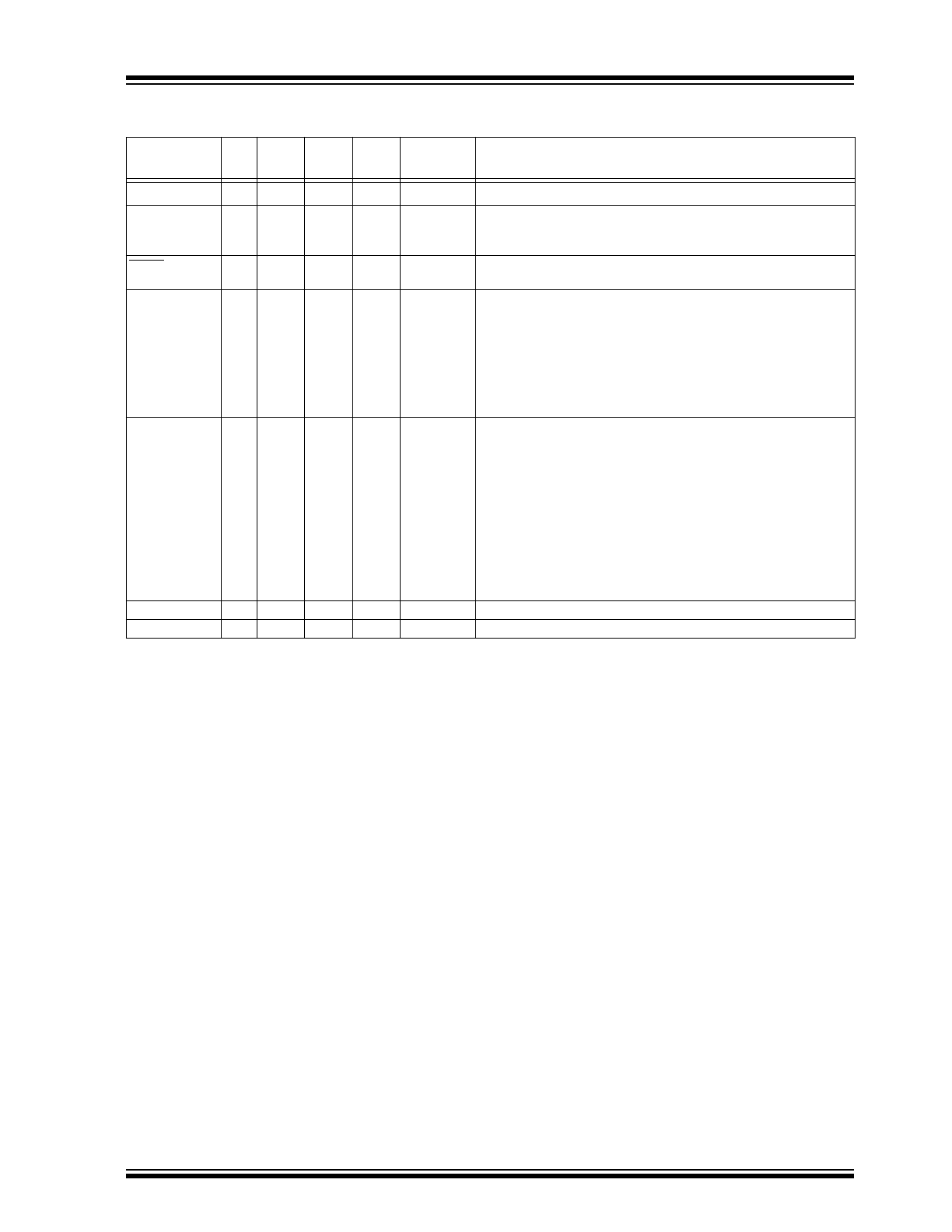
PIC16C710/71/711/715 PINOUT DESCRIPTION
Pin Name
DIP
Pin#
SSOP
Pin#
(4)
SOIC
Pin#
I/O/P
Type
Buffer
Type
Description
OSC1/CLKIN
16
18
16
I
ST/CMOS
(3)
Oscillator crystal input/external clock source input.
OSC2/CLKOUT
15
17
15
O
—
Oscillator crystal output. Connects to crystal or resonator in crystal
oscillator mode. In RC mode, OSC2 pin outputs CLKOUT which has
1/4 the frequency of OSC1, and denotes the instruction cycle rate.
MCLR/V
PP
4
4
4
I/P
ST
Master clear (reset) input or programming voltage input. This pin is
an active low reset to the device.
PORTA is a bi-directional I/O port.
RA0/AN0
17
19
17
I/O
TTL
RA0 can also be analog input0
RA1/AN1
18
20
18
I/O
TTL
RA1 can also be analog input1
RA2/AN2
1
1
1
I/O
TTL
RA2 can also be analog input2
RA3/AN3/V
REF
2
2
2
I/O
TTL
RA3 can also be analog input3 or analog reference voltage
RA4/T0CKI
3
3
3
I/O
ST
RA4 can also be the clock input to the Timer0 module. Output is
open drain type.
PORTB is a bi-directional I/O port. PORTB can be software pro-
grammed for internal weak pull-up on all inputs.
RB0/INT
6
7
6
I/O
TTL/ST
(1)
RB0 can also be the external interrupt pin.
RB1
7
8
7
I/O
TTL
RB2
8
9
8
I/O
TTL
RB3
9
10
9
I/O
TTL
RB4
10
11
10
I/O
TTL
Interrupt on change pin.
RB5
11
12
11
I/O
TTL
Interrupt on change pin.
RB6
12
13
12
I/O
TTL/ST
(2)
Interrupt on change pin. Serial programming clock.
RB7
13
14
13
I/O
TTL/ST
(2)
Interrupt on change pin. Serial programming data.
V
SS
5
4, 6
5
P
—
Ground reference for logic and I/O pins.
V
DD
14
15, 16
14
P
—
Positive supply for logic and I/O pins.
Legend: I = input
O = output
I/O = input/output
P = power
— = Not used
TTL = TTL input
ST = Schmitt Trigger input
Note 1:
This buffer is a Schmitt Trigger input when configured as the external interrupt.
2:
This buffer is a Schmitt Trigger input when used in serial programming mode.
3:
This buffer is a Schmitt Trigger input when configured in RC oscillator mode and a CMOS input otherwise.
4:
The PIC16C71 is not available in SSOP package.
PIC16C71X
DS30272A-page 10
1997 Microchip Technology Inc.
3.1
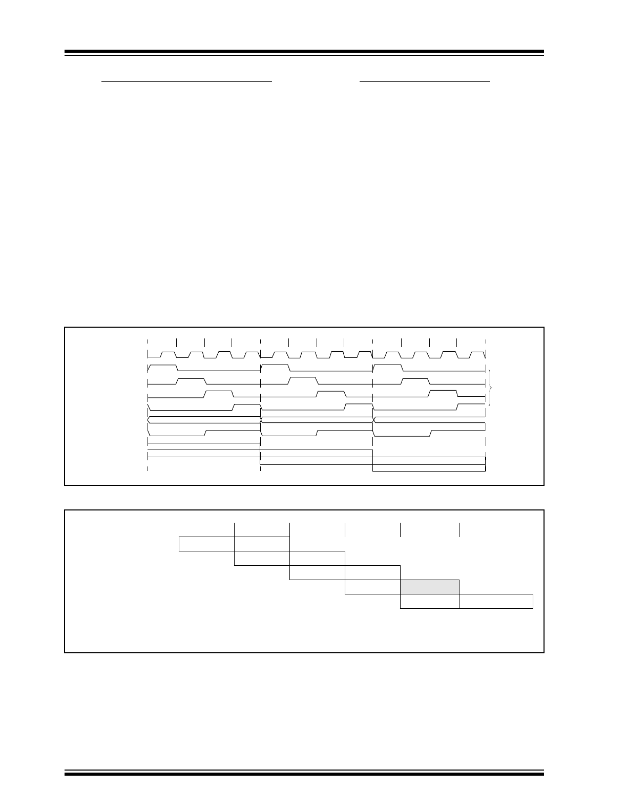
Clocking Scheme/Instruction Cycle
The clock input (from OSC1) is internally divided by
four to generate four non-overlapping quadrature
clocks namely Q1, Q2, Q3 and Q4. Internally, the pro-
gram counter (PC) is incremented every Q1, the
instruction is fetched from the program memory and
latched into the instruction register in Q4. The instruc-
tion is decoded and executed during the following Q1
through Q4. The clocks and instruction execution flow
is shown in Figure 3-2.
3.2
Instruction Flow/Pipelining
An “Instruction Cycle” consists of four Q cycles (Q1,
Q2, Q3 and Q4). The instruction fetch and execute are
pipelined such that fetch takes one instruction cycle
while decode and execute takes another instruction
cycle. However, due to the pipelining, each instruction
effectively executes in one cycle. If an instruction
causes the program counter to change (e.g.
GOTO
) then
two cycles are required to complete the instruction
(Example 3-1).
A fetch cycle begins with the program counter (PC)
incrementing in Q1.
In the execution cycle, the fetched instruction is latched
into the “Instruction Register” (IR) in cycle Q1. This
instruction is then decoded and executed during the
Q2, Q3, and Q4 cycles. Data memory is read during Q2
(operand read) and written during Q4 (destination
write).
FIGURE 3-2:
CLOCK/INSTRUCTION CYCLE
EXAMPLE 3-1:
INSTRUCTION PIPELINE FLOW
Q1
Q2
Q3
Q4
Q1
Q2
Q3
Q4
Q1
Q2
Q3
Q4
OSC1
Q1
Q2
Q3
Q4
PC
OSC2/CLKOUT
(RC mode)
PC
PC+1
PC+2
Fetch INST (PC)
Execute INST (PC-1)
Fetch INST (PC+1)
Execute INST (PC)
Fetch INST (PC+2)
Execute INST (PC+1)
Internal
phase
clock
All instructions are single cycle, except for any program branches. These take two cycles since the fetch
instruction is “flushed” from the pipeline while the new instruction is being fetched and then executed.
Tcy0
Tcy1
Tcy2
Tcy3
Tcy4
Tcy5
1. MOVLW 55h
Fetch 1
Execute 1
2. MOVWF PORTB
Fetch 2
Execute 2
3. CALL SUB_1
Fetch 3
Execute 3
4. BSF PORTA, BIT3 (Forced NOP)
Fetch 4
Flush
5. Instruction @ address SUB_1
Fetch SUB_1 Execute SUB_1