
1996 Microchip Technology Inc.
Preliminary
DS30559A-page 1
Devices included in this data sheet:
• PIC16C641
• PIC16C642
• PIC16C661
• PIC16C662
High Performance RISC CPU:
• Only 35 instructions to learn
• All single-cycle instructions (200 ns), except for
program branches which are two-cycle
• Operating speed:
- DC - 20 MHz clock input
- DC - 200 ns instruction cycle
• Interrupt capability
• 8-level deep hardware stack
• Direct, Indirect and Relative addressing modes
Peripheral Features:
• Up to 33 I/O pins with individual direction control
• High current sink/source for direct LED drive
• Analog comparator module with:
- Two analog comparators
- Programmable on-chip voltage reference
(V
REF
) module
- Programmable input multiplexing from device
inputs and internal voltage reference
- Comparator outputs can be output signals
• Timer0: 8-bit timer/counter with 8-bit
programmable prescaler
Special Microcontroller Features:
• Power-on Reset (POR)
• Power-up Timer (PWRT) and
Oscillator Start-up Timer (OST)
• Brown-out Reset
• Watchdog Timer (WDT) with its own on-chip RC
oscillator for reliable operation
• Programmable code protection
• Power saving SLEEP mode
• Selectable oscillator options
• Serial in-circuit programming (via two pins)
Device
Program
Memory x14
Data
Memory x8
PIC16C641
2K
128
PIC16C642
4K
176
PIC16C661
2K
128
PIC16C662
4K
176
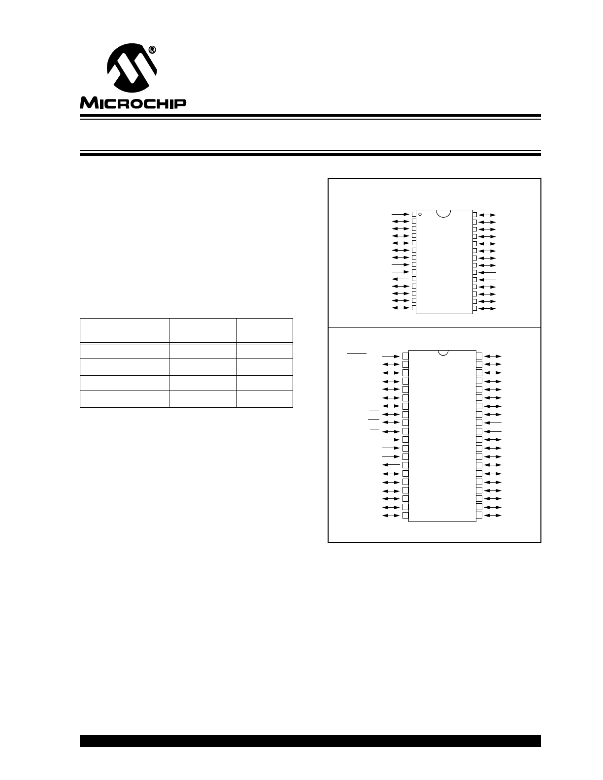
Pin Diagrams
PDIP, SOIC, Windowed CERDIP
RB7
RB6
RB5
RB4
RB3
RB2
RB1
RB0/INT
V
DD
V
SS
RC7
RC6
RC5
RC4
28
27
26
25
24
23
22
21
20
19
18
17
16
15
PIC16C64X
MCLR/V
PP
RA0/AN0
RA1/AN1
RA2/AN2/V
REF
RA3/AN3
RA4/T0CKI
RA5
V
SS
OSC1/CLKIN
OSC2/CLKOUT
RC0
RC1
1
2
3
4
5
6
7
8
9
10
11
12
13
14
RC2
RC3
PDIP, Windowed CERDIP
PIC16C66X
10
11
2
3
4
5
6
1
8
7
9
12
13
14
15
16
17
18
19
20
29
30
31
32
33
34
35
36
37
38
39
23
24
25
26
27
28
22
21
40
MCLR/V
PP
RA0/AN0
RA1/AN1
RA2/AN2/V
REF
RA3/AN3
RA4/T0CKI
RA5
RE0/RD
OSC1/CLKIN
OSC2/CLKOUT
RE1/WR
RE2/CS
V
DD
V
SS
RD0/PSP0
RD1/PSP1
RB7
RB6
RB5
RB4
RB3
RB2
RB1
RB0/INT
V
DD
V
SS
RD7/PSP7
RD6/PSP6
RD4/PSP4
RC7
RC6
RC5
RC4
RD3/PSP3
RD2/PSP2
RD5/PSP5
RC0
RC1
RC2
RC3
• Four user programmable ID locations
• Program Memory Parity Error checking circuitry
with Parity Error Reset (PER)
•
CMOS Technology:
• Low-power, high-speed CMOS EPROM technology
• Fully static design
• Wide operating voltage range: 3.0V to 6.0V
• Commercial, Industrial and Automotive
temperature ranges
• Low power consumption
- < 2.0 mA @ 5.0V, 4.0 MHz
- 15
µ
A typical @ 3.0V, 32 kHz
- < 1.0
µ
A typical standby current @ 3.0V
8-Bit EPROM Microcontrollers with Analog Comparators
PIC16C64X & PIC16C66X
This document was created with FrameMaker 4 0 4
PIC16C64X & PIC16C66X
DS30559A-page 2
Preliminary
1996 Microchip Technology Inc.
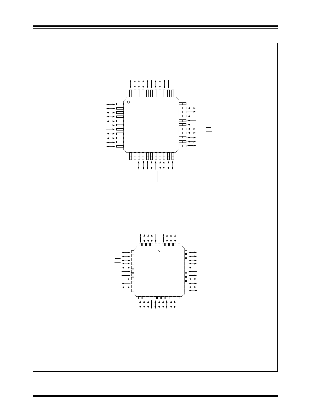
Pin Diagrams (Cont.’d)
10
11
12
13
14
15
16
17
18 19 20 21 2223 24 2526
44
8
7
6 5 4 3 2 1
27 28
29
30
31
32
33
34
35
36
37
38
39
40
41
42
43
9
PIC16C66X
RA4/T0CKI
RA5
RE0/RD
OSC1/CLKIN
OSC2/CLKOUT
RC0
NC
RE1/WR
RE2/CS
V
DD
V
SS
RB3
RB2
RB1
RB0/INT
V
DD
V
SS
RD7/PSP7
RD6/PSP6
RD5/PSP5
RD4/PSP4
RC7
RA3/AN3
RA2/AN2/V
REF
RA1/AN1
RA0/AN0
MCLR
/V
PP
NC
RB7
RB6
RB5
RB4 NC
NC
RC6
RC5
RC4
RD3/PSP3
RD2/PSP2
RD1/PSP1
RD0/PSP0
RC3
RC2
RC1
10
11
2
3
4
5
6
1
18 19 20 21 22
12 1314 15
38
8
7
44 43 42 41 40 39
16 17
29
30
31
32
33
23
24
25
26
27
28
36
34
35
9
PIC16C66X
37
RA3/AN3
RA2/AN2/V
REF
RA1/AN1
RA0/AN0
MCLR
/V
PP
NC
RB7
RB6
RB5
RB4
NC
RC6
RC5
RC4
RD3/PSP3
RD2/PSP2
RD1/PSP1
RD0/PSP0
RC3
RC2
RC1
NC
NC
RC0
OSC2/CLKOUT
OSC1/CLKIN
V
SS
V
DD
RE2/CS
RE1/WR
RE0/RD
RA5
RA4/T0CKI
RC7
RD4/PSP4
RD5/PSP5
RD6/PSP6
RD7/PSP7
V
SS
V
DD
RB0/INT
RB1
RB2
RB3
TQFP
PLCC

1996 Microchip Technology Inc.
Preliminary
DS30559A-page 3
PIC16C64X & PIC16C66X
Table of Contents
1.0
General Description .......................................................................................................................................... 5
2.0
PIC16C64X & PIC16C66X Device Varieties .................................................................................................... 7
3.0
Architectural Overview...................................................................................................................................... 9
4.0
Memory Organization ..................................................................................................................................... 17
5.0
I/O Ports.......................................................................................................................................................... 29
6.0
Timer0 Module................................................................................................................................................ 41
7.0
Comparator Module ........................................................................................................................................ 47
8.0
Voltage Reference Module ............................................................................................................................. 53
9.0
Special Features of the CPU .......................................................................................................................... 55
10.0
Instruction Set Summary ................................................................................................................................ 73
11.0
Development Support ..................................................................................................................................... 87
12.0
Electrical Specifications .................................................................................................................................. 91
13.0
Device Characterization Information............................................................................................................. 103
14.0
Packaging Information .................................................................................................................................. 105
Appendix A: Enhancements...................................................................................................................................... 115
Appendix B: Compatibility ......................................................................................................................................... 115
Appendix C: What’s New .......................................................................................................................................... 116
Appendix D: What’s Changed ................................................................................................................................... 116
Appendix E: PIC16/17 Microcontrollers ..................................................................................................................... 117
Pin Compatibility ......................................................................................................................................................... 125
Index ........................................................................................................................................................................... 127
List of Examples.......................................................................................................................................................... 129
List of Figures.............................................................................................................................................................. 129
List of Tables............................................................................................................................................................... 130
On-Line Support.......................................................................................................................................................... 131
Reader Response ....................................................................................................................................................... 132
PIC16C64X & PIC16C66X Product Identification System .......................................................................................... 135
To Our Valued Customers
We constantly strive to improve the quality of all our products and documentation. We have spent an exceptional
amount of time to ensure that these documents are correct. However, we realize that we may have missed a few
things. If you find any information that is missing or appears in error, please use the reader response form in the
back of this data sheet to inform us. We appreciate your assistance in making this a better document.

PIC16C64X & PIC16C66X
DS30559A-page 4
Preliminary
1996 Microchip Technology Inc.
NOTES:

1996 Microchip Technology Inc.
Preliminary
DS30559A-page 5
PIC16C64X & PIC16C66X
1.0
GENERAL DESCRIPTION
PIC16C64X & PIC16C66X devices are 28-pin and
40-pin EPROM-based members of the versatile
PIC16CXXX family of low-cost, high-performance,
CMOS, fully-static, 8-bit microcontrollers.
All PIC16/17 microcontrollers employ an advanced
RISC architecture. The PIC16CXXX family has
enhanced core features, eight-level deep stack, and
multiple internal and external interrupt sources. The
separate instruction and data buses of the Harvard
architecture allow a 14-bit wide instruction word with
the separate 8-bit wide data. The two-stage instruction
pipeline allows all instructions to execute in a sin-
gle-cycle, except for program branches (which require
two cycles). A total of 35 instructions (reduced instruc-
tion set) are available. Additionally, a large register set
gives some of the architectural innovations used to
achieve a very high performance.
PIC16CXXX microcontrollers typically achieve a 2:1
code compression and a 4:1 speed improvement over
other 8-bit microcontrollers in its class.
The PIC16C641 has 128 bytes of RAM and the
PIC16C642 has 176 bytes of RAM. Both devices have
22 I/O pins, and an 8-bit timer/counter with an 8-bit pro-
grammable prescaler. In addition, they have two analog
comparators with a programmable on-chip voltage ref-
erence module. Program Memory has internal parity
error detection circuitry with a Parity Error Reset. The
comparator module is ideally suited for applications
requiring a low-cost analog interface (e.g., battery
chargers, threshold detectors, white goods
controllers, etc.).
The PIC16C661 has 128 bytes of RAM and the
PIC16C662 has 176 bytes of RAM. Both devices have
33 I/O pins, and an 8-bit timer/counter with an 8-bit pro-
grammable prescaler. They also have an 8-bit Parallel
Slave Port. In addition, the devices have two analog
comparators with a programmable on-chip voltage ref-
erence module. Program Memory has internal parity
error detection circuitry with a Parity Error Reset. The
comparator module is ideally suited for applications
requiring a low-cost analog interface (e.g., battery
chargers, threshold detectors, white goods
controllers, etc.).
PIC16CXXX devices have special features to reduce
external components, thus reducing cost, enhancing
system reliability and reducing power consumption.
There are four oscillator options, of which the single pin
RC oscillator provides a low-cost solution, the LP
oscillator minimizes power consumption, XT is a
standard crystal, and the HS is for High Speed crystals.
The SLEEP (power-down) mode offers power saving.
The user can wake-up the chip from SLEEP through
several external and internal interrupts and resets.
A highly reliable Watchdog Timer (WDT) with its own
on-chip RC oscillator provides protection against soft-
ware lock-up.
A UV-erasable CERDIP-packaged version is ideal for
code development while the cost-effective One-Time
Programmable (OTP) version is suitable for production
in any volume.
The PIC16CXXX series fit perfectly in applications
ranging from battery chargers to low-power remote
sensors. The EPROM technology makes
customization of application programs (detection
levels, pulse generation, timers, etc.) extremely fast
and convenient. The small footprint packages make
this microcontroller series perfect for all applications
with space limitations. Low-cost, low-power,
high-performance, ease of use, and I/O flexibility make
the PIC16C64X & PIC16C66X very versatile.
1.1
Family and Upward Compatibility
Those users familiar with the PIC16C5X family of
microcontrollers will realize that this is an enhanced
version of the PIC16C5X architecture. Please refer to
Appendix A for a detailed list of enhancements. Code
written for PIC16C5X can be easily ported to the
PIC16C64X & PIC16C66X (Appendix B).
1.2
Development Support
PIC16C64X & PIC16C66X devices are supported by
the complete line of Microchip Development tools,
including:
• MPLAB Integrated Development Environment
including MPLAB-Simulator.
• MPASM Universal Assembler and MPLAB-C Uni-
versal C compiler.
• PRO MATE II and PICSTART Plus device pro-
grammers.
• PICMASTER In-circuit Emulator System
•
fuzzy
TECH-MP Fuzzy Logic Development Tools
• DriveWay Visual Programming Tool
Please refer to Section 11.0 for more details about
these and other Microchip development tools.
This document was created with FrameMaker 4 0 4
PIC16C64X & PIC16C66X
DS30559A-page 6
Preliminary
1996 Microchip Technology Inc.
TABLE 1-1:
PIC16C64X & PIC16C66X DEVICE FEATURES
PIC16C641
20
2K
128
TMR0
2
Yes
-
4
22
3.0-6.0
Yes
28-pin PDIP, SOIC, Windowed CDIP
PIC16C642
20
4K
176
TMR0
2
Yes
-
4
22
3.0-6.0
Yes
28-pin PDIP, SOIC, Windowed CDIP
PIC16C661
20
2K
128
TMR0
2
Yes
Yes
5
3
3
3.0-6.0
Yes
40-pin PDIP, Windowed CDIP;
44-pin PLCC, TQFP
PIC16C662
20
4K
176
TMR0
2
Yes
Yes
5
3
3
3.0-6.0
Yes
40-pin PDIP, Windowed CDIP;
44-pin PLCC, TQFP
All PIC16/17 Family devices have Power-on Reset, selectable W
atchdog
T
imer
, selectable code protect, and high I/O current
capability
.
All PIC16CXXX Family devices use serial programming with clock pin RB6 and data pin RB7.
Maximum Frequency of Operation (MHz)
EPROM
Data Memory (bytes)
Timer Module(s)
Comparator(s)
Internal Reference Voltage
Interrupt Sources
I/O Pins
Voltage Range (Volts)
Brown-out Reset
Packages
Program Memory
Clock
Memory
Peripherals
Features
Parallel Slave Port

1996 Microchip Technology Inc.
Preliminary
DS30559A-page 7
PIC16C64X & PIC16C66X
2.0
PIC16C64X & PIC16C66X
DEVICE VARIETIES
A variety of frequency ranges and packaging options
are available. Depending on application and production
requirements the proper device option can be selected
using the information in the Product Identification Sys-
tem page at the end of this data sheet. When placing
orders, please use that page of the data sheet to spec-
ify the correct part number.
2.1
UV Erasable Devices
The UV erasable version, offered in CERDIP package
is optimal for prototype development and pilot
programs. This version can be erased and
reprogrammed to any of the oscillator modes.
Microchip's PICSTART
Plus and PRO
MATE
II
programmers both support programming of the
PIC16C64X & PIC16C66X.
2.2
One-Time-Programmable (OTP)
Devices
The availability of OTP devices is especially useful for
customers who need flexibility for frequent code
updates and small volume applications. In addition to
the program memory, the configuration bits must also
be programmed.
2.3
Quick-Turnaround-Production (QTP)
Devices
Microchip offers a QTP Programming Service for
factory production orders. This service is made
available for users who choose not to program a
medium to high quantity of units and whose code pat-
terns have stabilized. The devices are identical to the
OTP devices but with all EPROM locations and config-
uration options already programmed by the factory.
Certain code and prototype verification procedures
apply before production shipments are available.
Please contact your Microchip Technology sales office
for more details.
2.4
Serialized Quick-Turnaround-
Production (SQTP
SM
) Devices
Microchip offers a unique programming service where
a few user-defined locations in each device are
programmed with different serial numbers. The serial
numbers may be random, pseudo-random or
sequential.
Serial programming allows each device to have a
unique number which can serve as an entry-code,
password or ID number.
This document was created with FrameMaker 4 0 4

PIC16C64X & PIC16C66X
DS30559A-page 8
Preliminary
1996 Microchip Technology Inc.
NOTES:

1996 Microchip Technology Inc.
Preliminary
DS30559A-page 9
PIC16C64X & PIC16C66X
3.0
ARCHITECTURAL OVERVIEW
The high performance of the PIC16C64X &
PIC16C66X devices can be attributed to a number of
architectural features commonly found in RISC micro-
processors. To begin with, the PIC16C64X &
PIC16C66X use a Harvard architecture in which pro-
gram and data are accessed from separate memories
using separate buses. This improves bandwidth over
traditional von Neumann architecture where program
and data are fetched from the same memory. Separat-
ing program and data memory further allows instruc-
tions to be sized differently than an 8-bit wide data
word. Instruction opcodes are 14-bits wide making it
possible to have all single word instructions. A 14-bit
wide program memory access bus fetches a 14-bit
instruction in a single cycle. A two-stage pipeline over-
laps fetch and execution of instructions. Consequently,
all instructions (35) execute in a single cycle (200 ns @
20 MHz) except for program branches, which require
two cycles.
The PIC16C641 and PIC16C661 both address 2K x 14
on-chip program memory while the PIC16C642 and
PIC16C662 address 4K x 14. All program memory is
internal.
PIC16C64X & PIC16C66X devices can directly or indi-
rectly address their register files or data memory. All
special function registers including the program
counter are mapped in the data memory. These
devices have an orthogonal (symmetrical) instruction
set that makes it possible to carry out any operation on
any register using any addressing mode. This symmet-
rical nature and lack of ‘special optimal situations’
make programming with the PIC16C64X & PIC16C66X
simple yet efficient. In addition, the learning curve is
reduced significantly.
PIC16C64X & PIC16C66X devices contain an 8-bit
ALU and working register. The ALU is a general pur-
pose arithmetic unit. It performs arithmetic and Bool-
ean functions between data in the working register and
any register file.
The ALU is 8-bits wide and capable of addition,
subtraction, shift, and logical operations. Unless
otherwise mentioned, arithmetic operations are two's
complement in nature. In two-operand instructions,
typically one operand is the working register
(W register). The other operand is a file register or an
immediate constant. In single operand instructions, the
operand is either the W register or a file register.
The W register is an 8-bit working register used for ALU
operations. It is not an addressable register.
Depending on the instruction executed, the ALU may
affect the values of the Carry (C), Digit Carry (DC), and
Zero (Z) bits in the STATUS register. The C and DC bits
operate as a Borrow and Digit Borrow out bit,
respectively, bit in subtraction. See the
SUBLW
and
SUBWF
instructions for examples.
This document was created with FrameMaker 4 0 4
PIC16C64X & PIC16C66X
DS30559A-page 10
Preliminary
1996 Microchip Technology Inc.
FIGURE 3-1:
PIC16C641/642 BLOCK DIAGRAM
EPROM
Program
Memory
13
Data Bus
8
14
Program
Bus
Instruction reg
Program Counter
8 Level Stack
(13-bit)
RAM
File
Registers
Direct Addr
7
RAM Bank
9
Addr MUX
Indirect
Addr
FSR reg
STATUS reg
MUX
ALU
W reg
Power-up
Timer
Oscillator
Start-up Timer
Power-on
Reset
Watchdog
Timer
Instruction
Decode &
Control
Timing
Generation
OSC1/CLKIN
OSC2/CLKOUT
MCLR
V
DD
, V
SS
Voltage
Brown-out
Reset
8
3
Timer0
PORTA
Comparator
RA3/AN3
RA2/AN2/V
REF
RA1/AN1
RA0/AN0
Reference
RA4/T0CKI
+
-
+
-
PORTB
RB0/INT
Select
RB1
RB2
RB3
RB4
RB5
RB6
RB7
PORTC
RC0
RC1
RC2
RC3
RC4
RC5
RC6
RC7
RA5
Parity Error
Reset
PIC16C641 has 2K x 14 Program Memory and 128 x 8 RAM
PIC16C642 has 4K x 14 Program Memory and 176 x 8 RAM