
2000-2013 Microchip Technology Inc.
Preliminary
DS41140C-page 1
PIC16C432
Devices included in this Data Sheet:
• PIC16C432
High Performance RISC CPU:
• Only 35 instructions to learn
• All single cycle instructions (200 ns), except for
program branches which are two-cycle
• Operating speed:
- DC - 20 MHz clock input
- DC - 200 ns instruction cycle
• Interrupt capability
• 16 special function hardware registers
• 8-level deep hardware stack
• Direct, Indirect and Relative Addressing modes
Peripheral Features:
• 12 I/O pins with individual direction control
• High current sink/source for direct LED drive
• Analog comparator module with:
- Two analog comparators
- Programmable on-chip voltage reference
(V
REF
) module
- Programmable input multiplexing from device
inputs and internal voltage reference
- Comparator outputs can be output signals
• Timer0: 8-bit timer/counter with 8-bit
programmable prescaler
• Integrated LIN Transceiver
• Wake-up on bus activity
• 12V battery operation for Transceiver
• Thermal shutdown for Transceiver
• Ground loss protection
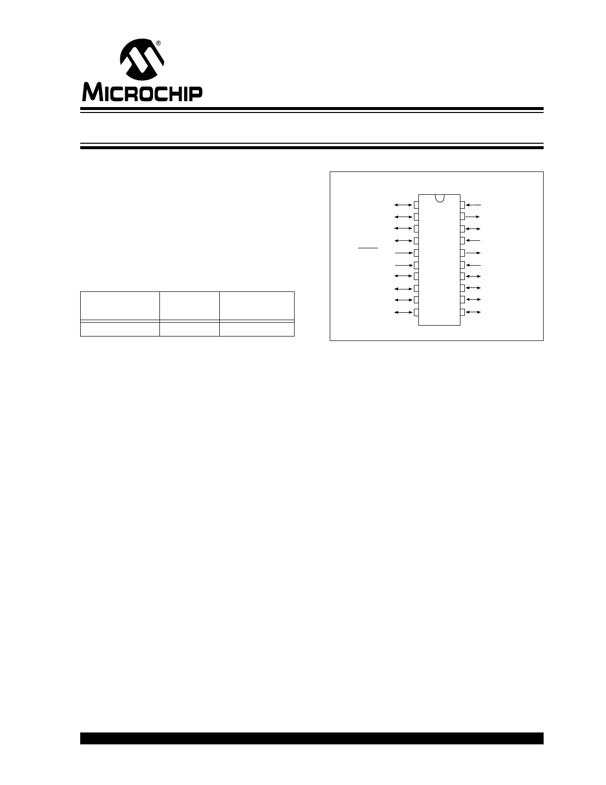
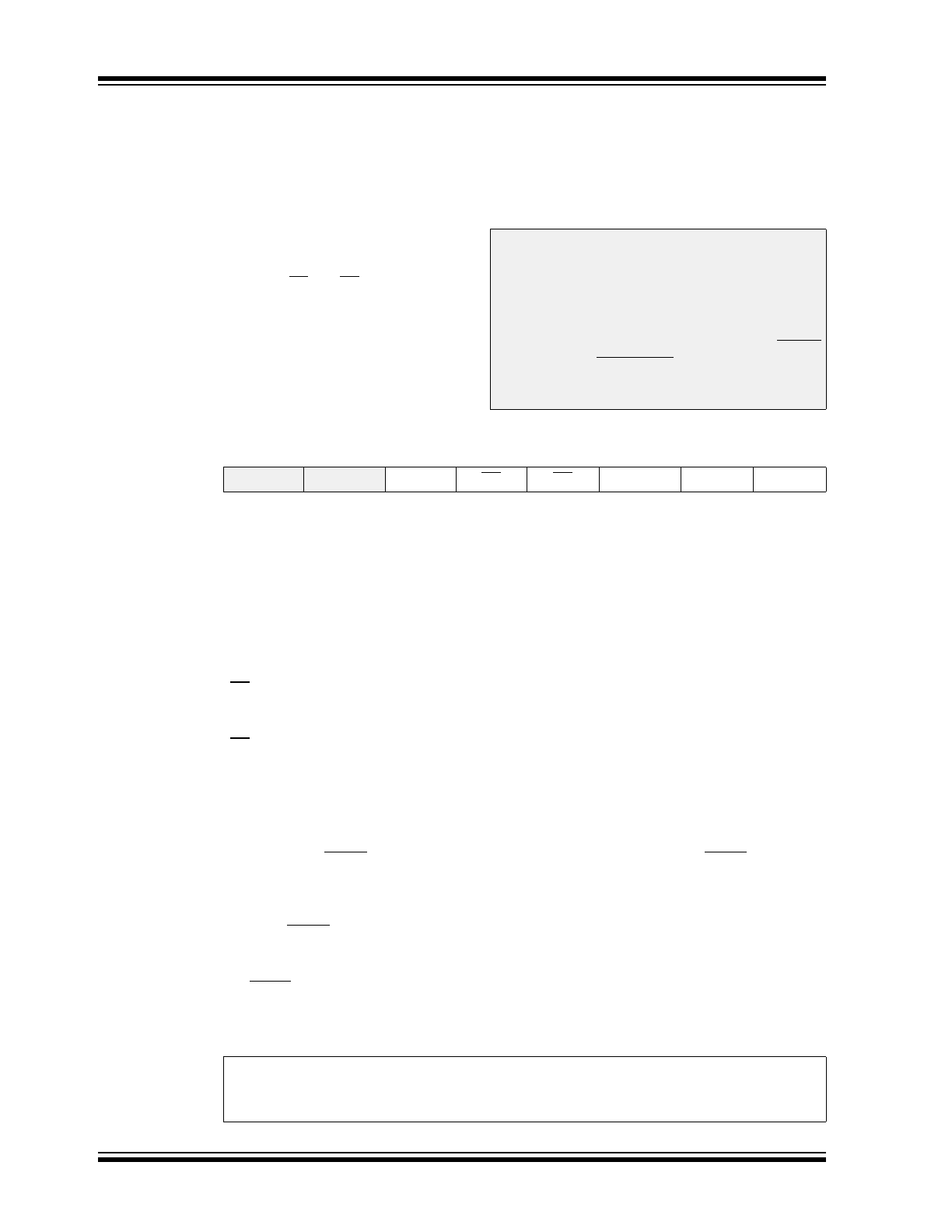
PIN DIAGRAM
Special Microcontroller Features:
• In-Circuit Serial Programming (ICSP™)
(via two pins)
• Power-on Reset (POR)
• Power-up Timer (PWRT) and Oscillator Start-up
Timer (OST)
• Brown-out Reset
• Watchdog Timer (WDT) with its own on-chip RC
oscillator for reliable operation
• Programmable code protection
• Power saving SLEEP mode
• Selectable oscillator options
• Four user programmable ID locations
CMOS Technology:
• Low power, high speed CMOS EPROM/HV-CMOS
technology
• Fully static design
• Operating voltage range
- 4.5V to 5.5V
• Industrial and extended temperature range
Device
Program
Memory
RAM Data
Memory
PIC16C432
2K x 14
128 x 8
Ceramic DIP, SSOP, PDIP
20
19
18
17
16
15
14
13
12
11
1
2
3
4
5
6
7
8
9
10
LIN
RA2/AN2/V
REF
RA3/AN3
RA4/T0CKI
MCLR/V
PP
V
SS
RB0/INT
RB1
RB2
RB3
V
BAT
V
SS
RA0/AN0
OSC1/CLKIN
OSC2/CLK-
OUT
V
DD
RB7
RB6
P
IC
1
6C
43
2
V
BAT
BACT
RA0/AN0
OSC1/CLKIN
OSC2/CLKOUT
V
DD
RB7
RB6
RB5
RB4
OTP 8-Bit CMOS MCU with LIN Transceiver

PIC16C432
DS41140C-page 2
Preliminary
2000-2013 Microchip Technology Inc.
Table of Contents
1.0
General Description...................................................................................................................................................................... 3
2.0
PIC16C432 Device Varieties ........................................................................................................................................................ 5
3.0
Memory Organization ................................................................................................................................................................... 7
4.0
I/O Ports ..................................................................................................................................................................................... 17
5.0
LIN Transceiver .......................................................................................................................................................................... 23
6.0
Timer0 Module ........................................................................................................................................................................... 27
7.0
Comparator Module.................................................................................................................................................................... 33
8.0
Voltage Reference Module ......................................................................................................................................................... 41
9.0
Special Features of the CPU ...................................................................................................................................................... 43
10.0 Instruction Set Summary ............................................................................................................................................................ 59
11.0 Development Support................................................................................................................................................................. 73
12.0 Electrical Specifications.............................................................................................................................................................. 79
13.0 DC and AC Characteristics Graphs and Tables ......................................................................................................................... 91
14.0 Packaging Information................................................................................................................................................................ 93
Appendix A:
Code for LIN Communication ...................................................................................................................................... 97
Index: .................................................................................................................................................................................................. 99
On-Line Support................................................................................................................................................................................. 101
Systems Information and Upgrade Hot Line ...................................................................................................................................... 101
Reader Response .............................................................................................................................................................................. 102
Product Identification System............................................................................................................................................................. 103
TO OUR VALUED CUSTOMERS
It is our intention to provide our valued customers with the best documentation possible to ensure successful use of your Microchip
products. To this end, we will continue to improve our publications to better suit your needs. Our publications will be refined and
enhanced as new volumes and updates are introduced.
If you have any questions or comments regarding this publication, please contact the Marketing Communications Department via
E-mail at docerrors@mail.microchip.com or fax the Reader Response Form in the back of this data sheet to (480) 792-4150.
We welcome your feedback.
Most Current Data Sheet
To obtain the most up-to-date version of this data sheet, please register at our Worldwide Web site at:
http://www.microchip.com
You can determine the version of a data sheet by examining its literature number found on the bottom outside corner of any page.
The last character of the literature number is the version number, (e.g., DS30000A is version A of document DS30000).
Errata
An errata sheet, describing minor operational differences from the data sheet and recommended workarounds, may exist for current
devices. As device/documentation issues become known to us, we will publish an errata sheet. The errata will specify the revision
of silicon and revision of document to which it applies.
To determine if an errata sheet exists for a particular device, please check with one of the following:
• Microchip’s Worldwide Web site; http://www.microchip.com
• Your local Microchip sales office (see last page)
• The Microchip Corporate Literature Center; U.S. FAX: (480) 792-7277
When contacting a sales office or the literature center, please specify which device, revision of silicon and data sheet (include liter-
ature number) you are using.
Customer Notification System
Register on our web site at www.microchip.com/cn to receive the most current information on all of our products.

2000-2013 Microchip Technology Inc.
Preliminary
DS41140C-page 3
PIC16C432
1.0
GENERAL DESCRIPTION
The PIC16C432 is a 20-pin EPROM-based member of
the versatile PIC
®
family of low cost, high performance,
CMOS, fully-static, 8-bit microcontrollers with an inte-
grated LIN transceiver.
The LIN physical layer is implemented in hardware with
a voltage range from 0V to 18V, with a 40V transient
capability. The LIN protocol is to be implemented in
firmware, which enables flexibility with future revisions
of the LIN protocol.
All PIC
®
microcontrollers employ an advanced RISC
architecture. The PIC16C432 device has enhanced
core features, eight-level deep stack, and multiple
internal and external interrupt sources. The separate
instruction and data buses of the Harvard architecture
allow a 14-bit wide instruction word with separate 8-bit
wide data. The two stage instruction pipeline allows all
instructions to execute in a single cycle, except for pro-
gram branches (which require two cycles). A total of 35
instructions (reduced instruction set) are available.
Additionally, a large register set gives some of the
architectural innovations used to achieve a very high
performance.
PIC16C432 microcontrollers typically achieve a 2:1
code compression and a 4:1 speed improvement over
other 8-bit microcontrollers in their class.
The PIC16C432 has 12 I/O pins and an 8-bit timer/
counter with an 8-bit programmable prescaler. In addi-
tion, the PIC16C432 adds two analog comparators with
a programmable on-chip voltage reference module.
The comparator module is ideally suited for applica-
tions requiring a low cost analog interface (e.g., battery
chargers, threshold detectors, white goods
controllers, etc.).
PIC16C432 devices have special features to reduce
external components, thus reducing system cost,
enhancing system reliability and reducing power con-
sumption. There are four oscillator options, of which the
single pin RC oscillator provides a low cost solution, the
LP oscillator minimizes power consumption, XT is a
standard crystal, and the HS is for High Speed crystals.
The SLEEP (power-down) mode offers power savings.
The user can wake-up the chip from SLEEP through
several external and internal interrupts and RESET.
A highly reliable Watchdog Timer with its own on-chip
RC oscillator provides protection against software lock-
up.
A UV erasable CERDIP packaged version is ideal for
code development, while the cost effective One-Time-
Programmable (OTP) version is suitable for production
in any volume.
A simplified block diagram of the PIC16C432 is shown
in Figure 4-1.
The PIC16C432 series fits perfectly in automotive and
industrial applications, which require LIN as a commu-
nication platform. The EPROM technology makes
customization of application programs (detection
levels, pulse generation, timers, etc.) extremely fast
and convenient. The small footprint packages make
this microcontroller series perfect for all applications
with space limitations. Low cost, low power, high per-
formance, ease of use and I/O flexibility make the
PIC16C432 very versatile.
1.1
Development Support
The PIC16C432 family is supported by a full-featured
macro assembler, a software simulator, an in-circuit
emulator, a low cost development programmer and a
full-featured programmer. A “C” compiler is also
available.

PIC16C432
DS41140C-page 4
Preliminary
2000-2013 Microchip Technology Inc.
NOTES:

2000-2013 Microchip Technology Inc.
Preliminary
DS41140C-page 5
PIC16C432
2.0
PIC16C432
DEVICE VARIETIES
A variety of frequency ranges and packaging options
are available. Depending on application and production
requirements, the proper device option can be selected
using the information in the PIC16C432 Product
Identification System section at the end of this data
sheet.
2.1
UV Erasable Devices
The UV erasable version, offered in the CERDIP pack-
age is optimal for prototype development and pilot
programs. This version can be erased and
reprogrammed to any of the oscillator modes.
Microchip's PRO MATE
®
programmers support pro-
gramming of the PIC16C432.
2.2
One-Time-Programmable (OTP)
Devices
The availability of OTP devices is especially useful for
customers who need the flexibility for frequent code
updates and small volume applications. In addition to
the program memory, the configuration bits must also
be programmed.
2.3
Quick-Turn-Programming (QTP)
Devices
Microchip offers a QTP Programming Service for
factory production orders. This service is made
available for users who choose not to program a
medium to high quantity of units and whose code pat-
terns have stabilized. The devices are identical to the
OTP devices, but with all EPROM locations and config-
uration options already programmed by the factory.
Certain code and prototype verification procedures
apply before production shipments are available.
Please contact your Microchip Technology sales office
for more details.
2.4
Serialized Quick-Turn-Programming
(SQTP
SM
) Devices
Microchip offers a unique programming service where
a few user defined locations in each device are
programmed with different serial numbers. The serial
numbers may be random, pseudo-random or
sequential.
Serial programming allows each device to have a
unique number which can serve as an entry code,
password or ID number.

PIC16C432
DS41140C-page 6
Preliminary
2000-2013 Microchip Technology Inc.
NOTES:
2000-2013 Microchip Technology Inc.
Preliminary
DS41140C-page 7
PIC16C432
3.0
MEMORY ORGANIZATION
3.1
Program Memory Organization
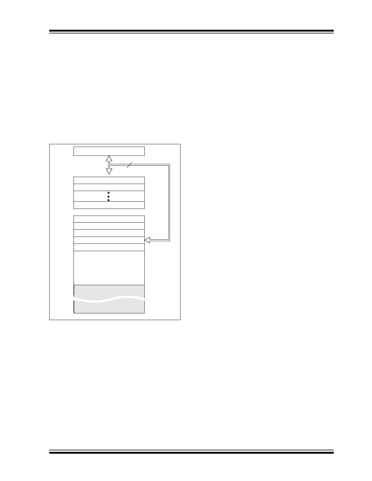
The PIC16C432 has a 13-bit program counter capable
of addressing an 8K x 14 program memory space. Only
the first 2K x 14 (0000h - 07FFh) are implemented for
the PIC16C432. Accessing a location above these
boundaries will cause a wrap-around within the first 2K
x 14 space. The RESET Vector is at 0000h and the
Interrupt Vector is at 0004h (Figure 3-1).
FIGURE 3-1:
PROGRAM MEMORY MAP
AND STACK FOR THE
PIC16C432
3.2
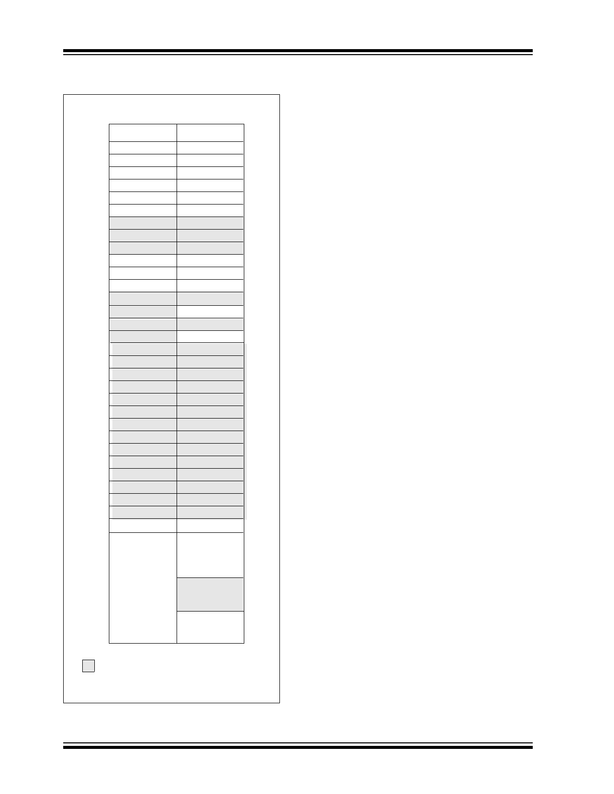
Data Memory Organization
The data memory (Figure 3-2) is partitioned into two
Banks, which contain the General Purpose Registers
and the Special Function Registers. Bank 0 is selected
when the RP0 bit is cleared. Bank 1 is selected when
the RP0 bit (STATUS <5>) is set. The Special Function
Registers are located in the first 32 locations of each
Bank. Register locations 20-7Fh (Bank 0) and A0-BFh
(Bank 1) are General Purpose Registers implemented
as static RAM. Some special purpose registers are
mapped in Bank 1. In the microcontroller, address
space F0h-FFh (Bank 1) is mapped to 70-7Fh (Bank 0)
as common RAM.
3.2.1
GENERAL PURPOSE REGISTER
FILE
The register file is organized as 128 x 8 in the
PIC16C432. Each is accessed either directly or indi-
rectly through the File Select Register FSR
(Section 3.4).
PC<12:0>
13
000h
0004h
0005h
07FFh
0800h
1FFFh
Stack Level 1
Stack Level 8
RESET Vector
Interrupt Vector
On-chip Program
Memory
CALL, RETURN
RETFIE, RETLW
Stack Level 2
PIC16C432
DS41140C-page 8
Preliminary
2000-2013 Microchip Technology Inc.
FIGURE 3-2:
DATA MEMORY MAP FOR
THE PIC16C432
3.2.2
SPECIAL FUNCTION REGISTERS
The Special Function Registers are registers used by
the CPU and peripheral functions for controlling the
desired operation of the device (Table 3-1). These
registers are static RAM.
The special registers can be classified into two sets
(core and peripheral). The Special Function Registers
associated with the “core” functions are described in
this section. Those related to the operation of the
peripheral features are described in the section of that
peripheral feature.
INDF
(1)
TMR0
PCL
STATUS
FSR
PORTA
PORTB
PCLATH
INTCON
PIR1
CMCON
INDF
(1)
OPTION
PCL
STATUS
FSR
TRISA
TRISB
PCLATH
INTCON
PIE1
PCON
VRCON
00h
01h
02h
03h
04h
05h
06h
07h
08h
09h
0Ah
0Bh
0Ch
0Dh
0Eh
0Fh
10h
11h
12h
13h
14h
15h
16h
17h
18h
19h
1Ah
1Bh
1Ch
1Dh
1Eh
1Fh
80h
81h
82h
83h
84h
85h
86h
87h
88h
89h
8Ah
8Bh
8Ch
8Dh
8Eh
8Fh
90h
91h
92h
93h
94h
95h
96h
97h
98h
99h
9Ah
9Bh
9Ch
9Dh
9Eh
9Fh
20h
A0h
General
Purpose
Register
7Fh
FFh
Bank 0
Bank 1
File
Address
BFh
C0h
Unimplemented data memory locations,read
as '0'.
Note 1: Not a physical register.
File
Address
General
Purpose
Register
Accesses
70h-7Fh
F0h
LININTF
2000-2013 Microchip Technology Inc.
Preliminary
DS41140C-page 9
PIC16C432
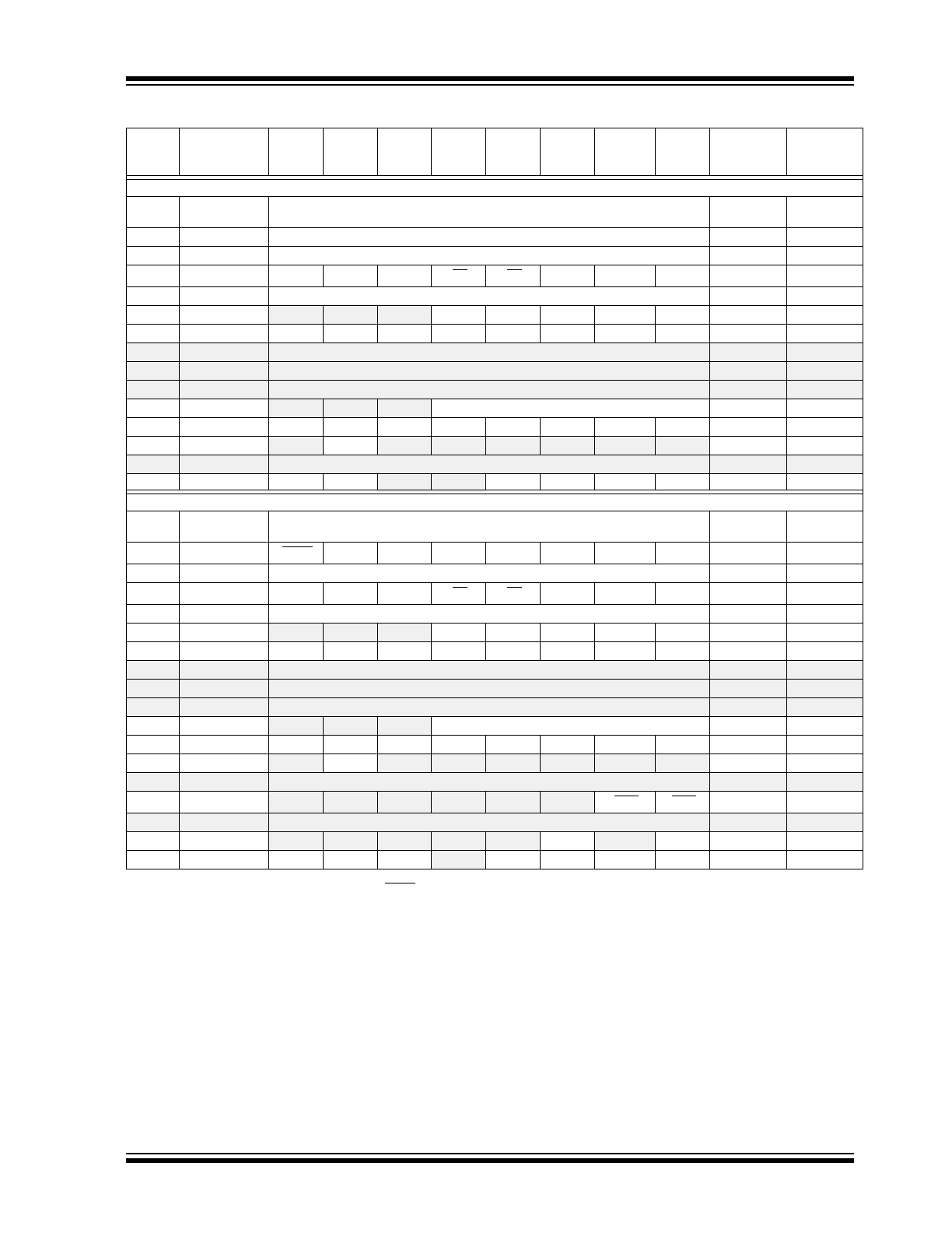
TABLE 3-1:
SPECIAL REGISTERS FOR THE PIC16C432
Address
Name
Bit 7
Bit 6
Bit 5
Bit 4
Bit 3
Bit 2
Bit 1
Bit 0
Value on
POR Reset
Value on all
other
RESETS
(1)
Bank 0
00h
INDF
Addressing this location uses contents of FSR to address data memory (not a physical
register)
xxxx xxxx
16
01h
TMR0
Timer0 Module’s Register
xxxx xxxx
27
02h
PCL
Program Counter's (PC) Least Significant Byte
0000 0000
15
03h
STATUS
IRP
(2)
RP1
(2)
RP0
TO
PD
Z
DC
C
0001 1xxx
10
04h
FSR
Indirect data memory address pointer
xxxx xxxx
16
05h
PORTA
—
—
—
RA4
RA3
RA2
LINRX
RA0
---x 0000
17
06h
PORTB
RB7
RB6
RB5
RB4
RB3
RB2
RB1
RB0
xxxx xxxx
20
07h
—
Unimplemented
—
—
08h
—
Unimplemented
—
—
09h
—
Unimplemented
—
—
0Ah
PCLATH
—
—
—
Write buffer for upper 5 bits of program counter
---0 0000
15
0Bh
INTCON
GIE PEIE
T0IE
INTE
RBIE
T0IF
INTF
RBIF
0000 000x
12
0Ch
PIR1
—
CMIF
—
—
—
—
—
—
-0-- ----
13
0Dh-1Eh
—
Unimplemented
—
—
1Fh
CMCON
C2OUT
C1OUT
—
—
CIS
CM2
CM1
CM0
00-- 0000
33
Bank 1
80h
INDF
Addressing this location uses contents of FSR to address data memory (not a physical
register)
xxxx xxxx
16
81h
OPTION_REG
RBPU
INTEDG
T0CS
T0SE
PSA
PS2
PS1
PS0
1111 1111
11
82h
PCL
Program Counter's (PC) Least Significant Byte
0000 0000
15
83h
STATUS
IRP
RP1
RP0
TO
PD
Z
DC
C
0001 1xxx
10
84h
FSR
Indirect data memory address pointer
xxxx xxxx
16
85h
TRISA
—
—
—
TRISA4
TRISA3
TRISA2
TLINRX
(3)
TRISA0
---1 1111
17
86h
TRISB
TRISB7
TRISB6
TRISB5
TRISB4
TRISB3
TRISB2
TRISB1
TRISB0
1111 1111
20
87h
—
Unimplemented
—
—
88h
—
Unimplemented
—
—
89h
—
Unimplemented
—
—
8Ah
PCLATH
—
—
—
Write buffer for upper 5 bits of program counter
---0 0000
15
8Bh
INTCON
GIE
PEIE
T0IE
INTE
RBIE
T0IF
INTF
RBIF
0000 000x
12
8Ch
PIE1
—
CMIE
—
—
—
—
—
—
-0-- ----
13
8Dh
—
Unimplemented
—
—
8Eh
PCON
—
—
—
—
—
—
POR
BOD
---- --0x
14
8Fh-9Eh
—
Unimplemented
—
—
90h
LININTF
—
—
—
—
—
LINTX
—
LINV
DD
---- -1-1
23
9Fh
VRCON
VREN
VROE
VRR
—
VR3
VR2
VR1
VR0
000- 0000
41
Legend:
— = Unimplemented locations read as ‘0’, u = unchanged, x = unknown, q = value depends on condition, shaded = unimplemented
Note
1:
Other (non power-up) RESETS include MCLR Reset, Brown-out Reset and Watchdog Timer Reset during normal operation.
2:
IRP & RPI bits are reserved; always maintain these bits clear.
3:
TLINRX must set to ‘1’ at all times.
PIC16C432
DS41140C-page 10
Preliminary
2000-2013 Microchip Technology Inc.
3.2.2.1
STATUS Register
The STATUS register, shown in Register 3-1, contains
the arithmetic status of the ALU, the RESET status and
the bank select bits for data memory.
The STATUS register can be the destination for any
instruction, like any other register. If the STATUS
register is the destination for an instruction that affects
the Z, DC or C bits, then the write to these three bits is
disabled. These bits are set or cleared according to the
device logic. Furthermore, the TO and PD bits are not
writable. Therefore, the result of an instruction with the
STATUS register as destination may be different than
intended.
For example, CLRF STATUS will clear the upper-three
bits and set the Z bit. This leaves the STATUS register
as 000uu1uu (where u = unchanged).
It is recommended, therefore, that only BCF, BSF,
SWAPF
and MOVWF instructions are used to alter the
STATUS register, because these instructions do not
affect any STATUS bit. For other instructions, not
affecting any STATUS bits, see the “Instruction Set
Summary”.
REGISTER 3-1:
STATUS REGISTER (ADDRESS 03h OR 83h)
Note 1: The IRP and RP1 bits (STATUS<7:6>)
are not used by the PIC16C432 and
should be programmed as ’0'. Use of
these bits as general purpose R/W bits is
NOT recommended, since this may affect
upward compatibility with future products.
2: The C and DC bits operate as a Borrow
and Digit Borrow out bit, respectively, in
subtraction. See the SUBLW and SUBWF
instructions for examples.
Reserved
Reserved
R/W-0
R-1
R-1
R/W-x
R/W-x
R/W-x
IRP
RP1
RP0
TO
PD
Z
DC
C
bit7
bit0
bit 7
IRP:
The IRP bit is reserved on the PIC16C432, always maintain this bit clear
bit 6-5
RP1:RP0: Register Bank Select bits (used for direct addressing)
11
= Bank 3 (180h - 1FFh)
10
= Bank 2 (100h - 17Fh)
01
= Bank 1 (80h - FFh)
00
= Bank 0 (00h - 7Fh)
Each bank is 128 bytes. The RP1 bit is reserved, always maintain this bit clear.
bit 4
TO: Timeout bit
1
= After power-up, CLRWDT instruction, or SLEEP instruction
0
= A WDT timeout occurred
bit 3
PD: Power-down bit
1
= After power-up or by the CLRWDT instruction
0
= By execution of the SLEEP instruction
bit 2
Z
: Zero bit
1
= The result of an arithmetic or logic operation is zero
0
= The result of an arithmetic or logic operation is not zero
bit 1
DC: Digit carry/borrow bit (ADDWF, ADDLW, SUBLW, SUBWF instructions) (for borrow the polarity
is reversed)
1
= A carry-out from the 4th low order bit of the result occurred
0
= No carry-out from the 4th low order bit of the result
bit 0
C: Carry/borrow bit (ADDWF, ADDLW, SUBLW, SUBWF instructions)
1
= A carry-out from the Most Significant bit of the result occurred
0
= No carry-out from the Most Significant bit of the result occurred
Note 1: For borrow, the polarity is reversed. A subtraction is executed by adding the two’s complement of
the second operand. For rotate (RRF, RLF) instructions, this bit is loaded with either the high or
low order bit of the source register.
Legend:
R = Readable bit
W = Writable bit
U = Unimplemented bit, read as ‘0’
- n = Value at POR reset
’1’ = Bit is set
’0’ = Bit is cleared
x = Bit is unknown