
1996 Microchip Technology Inc.
Preliminary
DS40122B-page 1
High-Performance RISC CPU:
• Only 35 single word instructions to learn
• All single cycle instructions except for program
branches which are two cycle
• Operating speed: DC - 20 MHz clock input
• 4096 x 14 on-chip EPROM program memory
• 192 x 8 general purpose registers (SRAM)
• 6 internal and 5 external interrupt sources
• 38 special function hardware registers
• Eight-level hardware stack
Analog Peripherals Features:
• Slope Analog-to-Digital (A/D) converter
- Eight external input channels including two
channels with selectable level shift inputs
- Six internal input channels
- 16-bit programmable timer with capture
register
- 16 ms maximum conversion time at maxi-
mum (16-bit) resolution and 4 MHz clock
- 4-bit programmable current source
• Internal bandgap voltage reference
• Factory calibrated with calibration constants
stored in EPROM
• On-chip temperature sensor
• Voltage regulator control output
• Two comparators with programmable references
• On-chip low voltage detector
Special Microcontroller Features:
• Power-on Reset (POR), Power-up Timer (PWRT)
and Oscillator Start-up Timer (OST)
• Watchdog Timer (WDT) with its own on-chip RC
oscillator for reliable operation
• Multi-segment programmable code-protection
• Selectable oscillator options
- Internal 4 MHz oscillator
- External crystal oscillator
• Serial in-system programming (via two pins)
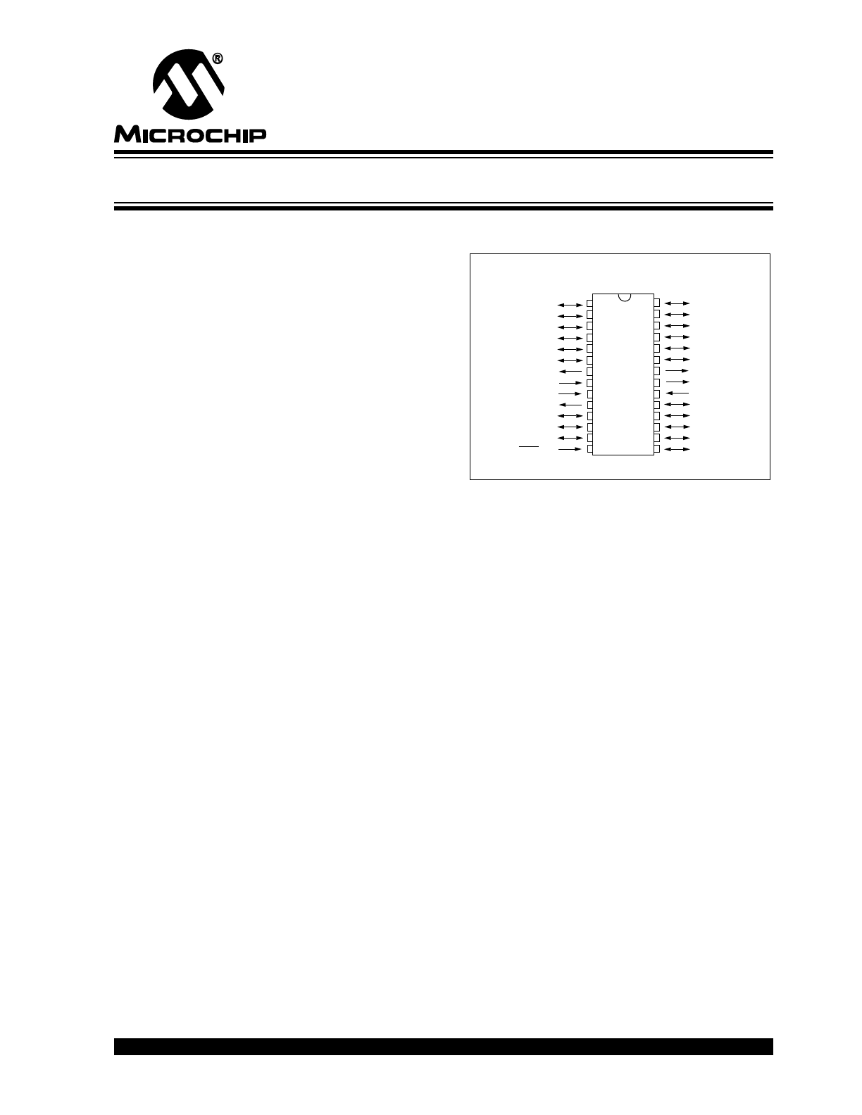
PIC14000
28-Pin Programmable Mixed Signal Controller
Pin Diagram
Digital Peripherals Features:
• 22 I/O pins with individual direction control
• High current sink/source for direct LED drive
• TMR0: 8-bit timer/counter with 8-bit
programmable prescaler
• 16-bit A/D timer: can be used as a general
purpose timer
• I
2
C
serial port compatible with System
Management Bus
CMOS Technology:
• Low-power, high-speed CMOS EPROM technology
• Fully static design
• Wide-operating voltage range (2.7V to 6.0V)
• Commercial and Industrial Temperature Range
• Low power dissipation (typical)
- < 3 mA @5V, 4 MHz operating mode
- < 300
µ
A @3V (Sleep mode: clocks stopped
with analog circuits active)
- < 5
µ
A @3V (Hiber nate mode: clocks
stopped, analog inactive, and WDT disabled)
Applications:
• Battery Chargers
• Battery Capacity Monitoring
• Uninterruptable Power Supply Controllers
• Power Management Controllers
• HVAC Controllers
• Sensing and Data Acquisition
PDIP, SOIC, SSOP, Windowed CERDIP
28
27
26
25
24
23
22
21
20
19
18
17
16
15
RA2/AN2
RA3/AN3
RD4/AN4
RD5/AN5
RD6/AN6
RD7/AN7
CDAC
SUM
V
SS
RC0/REFA
RC1/CMPA
RC2
RC3/T0CKI
RC4
PIC14000
• 1
2
3
4
5
6
7
8
9
10
11
12
13
14
RA1/AN1
RA0/AN0
RD3/REFB
RD2/CMPB
RD1/SDAB
RD0/SCLB
OSC2/CLKOUT
OSC1/PBTN
V
DD
VREG
RC7/SDAA
RC6/SCLA
RC5
MCLR/V
PP
This document was created with FrameMaker 4 0 4

PIC14000
DS40122B-page 2
Preliminary
1996 Microchip Technology Inc.
TABLE OF CONTENTS
1.0:
General Description........................................................................................................................... 3
2.0:
Device Varieties ................................................................................................................................ 5
3.0:
Architectural Overview ...................................................................................................................... 7
4.0:
Memory Organization ...................................................................................................................... 13
5.0:
I/O Ports .......................................................................................................................................... 25
6.0:
Timer Modules................................................................................................................................. 37
7.0:
Inter-integrated Circuit Serial Port (I
2
C
)........................................................................................ 41
8.0:
Analog Modules for A/D Conversion ............................................................................................... 57
9.0:
Other Analog Modules..................................................................................................................... 65
10.0: Special Features of the CPU ........................................................................................................... 75
11.0: Instruction Set Summary ................................................................................................................. 91
12.0: Development Support.................................................................................................................... 103
13.0: Electrical Characteristics for PIC14000 ..........................................................................................107
14.0: Analog Specifications: PIC14000-04 (Commercial, Industrial)...................................................... 123
Appendix A:PIC16/17 Microcontrollers ....................................................................................................133
Index .........................................................................................................................................................143
PIC14000 Product Identification System ..................................................................................................149
To Our Valued Customers
We constantly strive to improve the quality of all our products and documentation. To this end, we recently converted
to a new publishing software package which we believe will enhance our entire documentation process and product.
As in any conversion process, information may have accidently been altered or deleted. We have spent an excep-
tional amount of time to ensure that these documents are correct. However, we realize that we may have missed a
few things. If you find any information that is missing or appears in error, please use the reader response form in the
back of this data sheet to inform us. We appreciate your assistance in making this a better document.

1996 Microchip Technology Inc.
Preliminary
DS40122B-page 3
PIC14000
1.0
GENERAL DESCRIPTION
The PIC14000 features include medium to high reso-
lution A/D conversion (10 to 16 bits), temperature sens-
ing, closed loop charge control, serial communication,
and low power operation.
The PIC14000 uses a RISC Harvard architecture CPU
with separate 14-bit instruction and 8-bit data buses. A
two-stage instruction pipeline allows all instructions to
execute in a single cycle, except for program branches,
which require two cycles. A total of 35 instructions are
available. Additionally, a large register set is included.
PIC16/17 microcontrollers typically achieve a 2:1 code
compression and a 4:1 speed improvement over other
8-bit microcontrollers.
Features:
The PIC14000 is a 28-pin device with these features:
• 4K of EPROM
• 192 bytes of RAM
• 22 I/O pins
The analog peripherals include:
• 8 external analog input channels, two with level
shift inputs
• 6 internal analog input channels
• 2 comparators with programmable references
• A bandgap reference
• An internal temperature sensor
• A programmable current source
In addition, the I
2
C serial port through a multiplexer
supports two separate I
2
C channels.
A special oscillator option allows either an internal
4 MHz oscillator or an external crystal oscillator. Using
the internal 4 MHz oscillator requires no external com-
ponents.
The PIC14000 contains three timers, the Watchdog
Timer (WDT), Timer0 (TMR0), and A/D Timer
(ADTMR). The Watchdog Timer includes its own
on-chip RC oscillator providing protection against
software lock-up. TMR0 is a general purpose 8-bit
timer/counter with an 8-bit prescaler. It may be clocked
externally using the RC3/T0CKI pin. The ADTMR is
intended for use with the slope A/D converter, but can
also be used as a general purpose timer. It has an
associated capture register which can be used to mea-
sure the time between events.
An internal low-voltage detect circuit allows for tracking
of voltage levels. Upon detecting the low voltage con-
dition, the PIC14000 can be instructed to save its oper-
ating state then enter an idle state.
The internal band-gap reference is used for calibrating
the measurements of the analog peripherals. The
calibration factors are stored in EPROM and can be
used to achieve high measurement accuracy.
Power savings modes are available for portable appli-
cations. The SLEEP and HIBERNATE modes offer dif-
ferent levels of power savings. The PIC14000 can
wake up from these modes through interrupts or reset.
A UV erasable CERDIP packaged version is ideal for
code development, while the cost-effective One-Time
Programmable (OTP) version is suitable for production
in any volume.
The PIC14000 fits perfectly in applications for battery
charging, capacity monitoring, and data logging. The
EPROM technology makes customization of
application programs (battery characteristics, feature
sets, etc.) extremely fast and convenient. The small
footprint packages make this microcontroller based
mixed signal device perfect for all applications with
space limitations. Low-cost, low-power, high perfor-
mance, ease of use and I/O flexibility make the
PIC14000 very versatile in other applications such as
temperature monitors/controllers.
1.1
Family and Upward Compatibility
Code written for PIC16C6X/7X can be easily ported to
the PIC14000 (see Appendix A).
1.2
Development Support
The PIC14000 is supported by a full-featured macro
assembler, a software simulator, an in-circuit emulator,
a low-cost development programmer and a
full-featured programmer. A “C” compiler and fuzzy
logic support tools are also available.
This document was created with FrameMaker 4 0 4

PIC14000
DS40122B-page 4
Preliminary
1996 Microchip Technology Inc.
NOTES:

1996 Microchip Technology Inc.
Preliminary
DS40122B-page 5
PIC14000
2.0
DEVICE VARIETIES
A variety of frequency ranges and packaging options
are available. The PIC14000 Product Selection System
section at the end of this data sheet provides the
devices options to be selected for your specific applica-
tion and production requirements. When placing
orders, please use the “PIC14000 Product Identifica-
tion System” at the back of this data sheet to specify the
correct part number.
2.1
UV Erasable Devices
The UV erasable version, offered in CERDIP package,
is optimal for prototype development and pilot
programs.
The UV erasable version can be erased and
reprogrammed to any of the configuration modes.
Microchip's PICSTART
,
PICSTART-PLUS and
PRO MATE
programmers all support programming of
the PIC14000. Third party programmers also are avail-
able; refer to the
Microchip
Third Party Guide
for a list
of sources.
2.2
One-Time-Programmable (OTP)
Devices
The availability of OTP devices is especially useful for
customers who need the flexibility for frequent code
updates or small volume applications.
The OTP devices, packaged in plastic packages permit
the user to program them once. In addition to the
program memory, the configuration bits must also be
programmed.
Note:
Please note that erasing the device will
also erase the pre-programmed calibration
factors. Please refer to AN621 for more
information.
2.3
Quick-Turnaround-Production (QTP)
Devices
Microchip offers a QTP Programming Service for
factory production orders. This service is made
available for users who choose not to program a
medium to high quantity of units and whose code
patterns have stabilized. The devices are identical to
the OTP devices but with all EPROM locations and
fuse options already programmed by the factory.
Certain code and prototype verification procedures do
apply before production shipments are available.
Please contact your local Microchip Technology sales
office for more details.
2.4
Serialized Quick-Turnaround
Production (SQTP
SM
) Devices
Microchip offers a unique programming service where
a few user-defined locations in each device are
programmed with different serial numbers. The serial
numbers may be random, pseudo-random or
sequential.
Serial programming allows each device to have a
unique number which can serve as an entry-code,
password or ID number.
This document was created with FrameMaker 4 0 4

PIC14000
DS40122B-page 6
Preliminary
1996 Microchip Technology Inc.
NOTES:

1996 Microchip Technology Inc.
Preliminary
DS40122B-page 7
PIC14000
3.0
ARCHITECTURAL OVERVIEW
The PIC14000 addresses 4K x 14 program memory. All
program memory is internal. The PIC14000 can directly
or indirectly address its register files or data memory. All
special function registers including the program counter
are mapped in the data memory. The PIC14000 has an
orthogonal instruction set that makes it possible to
carry out any operation on any register using any
addressing mode. This symmetrical nature and lack of
‘special optimal situations’ make programming with the
PIC14000 simple yet efficient. In addition, the learning
curve is reduced significantly.
The PIC14000 contains an 8-bit ALU and working
register. The ALU performs arithmetic and Boolean
functions between data in the working register and any
register file.
The ALU is capable of addition, subtraction, shift, and
logical operations. Unless otherwise mentioned,
arithmetic operations are two's complement. In
two-operand instructions, typically one operand is the
working register (W register). The other operand is a
file register or an immediate constant. In single
operand instructions, the operand is either the
W register or a file register.
Depending on the instruction executed, the ALU may
affect the values of the Carry (C), Digit Carry (DC), and
Zero (Z) bits in the STATUS register. The C and DC bits
operate as a borrow bit and a digit borrow out bit,
respectively, in subtraction. See the
SUBLW
and
SUBWF
instructions for examples.
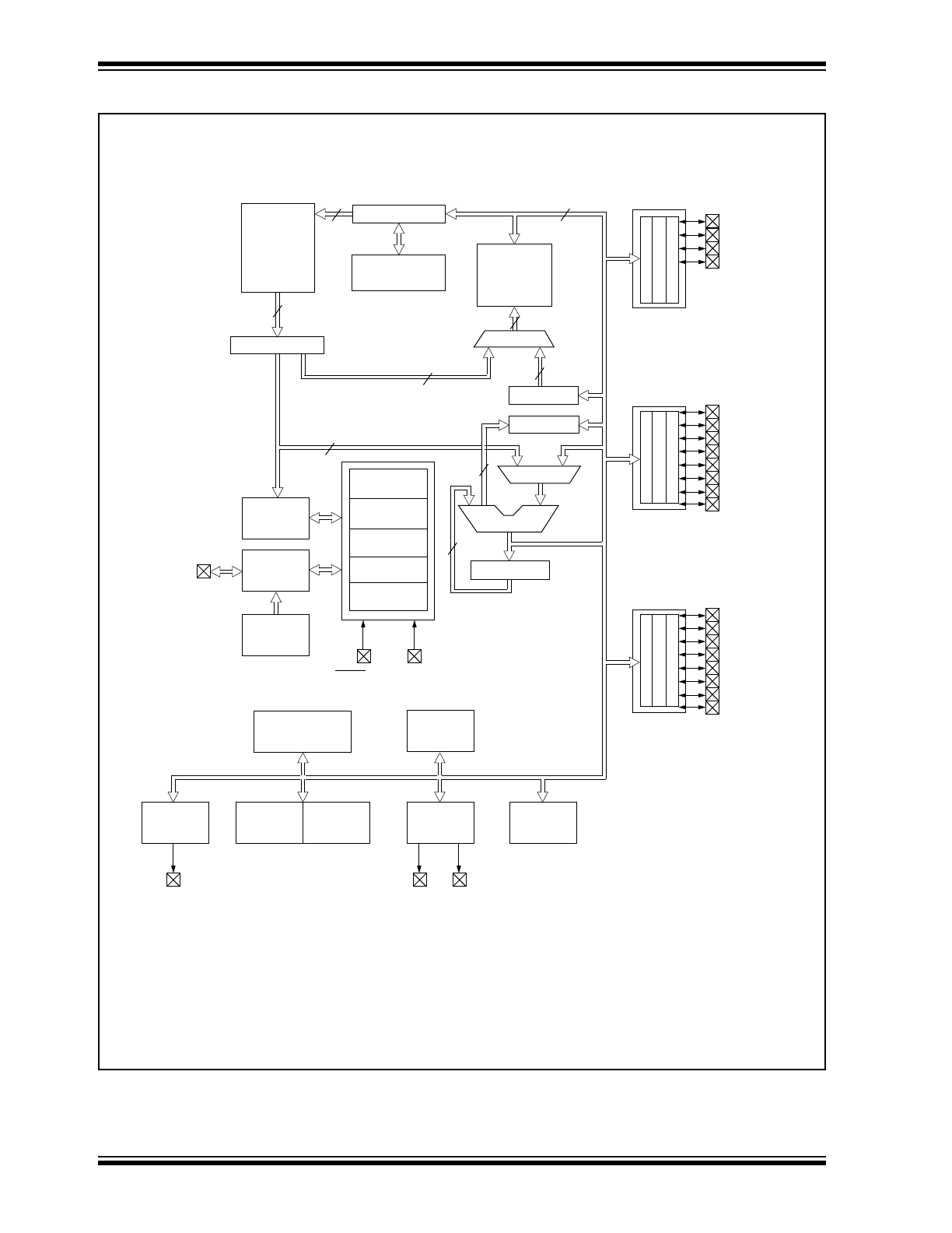
A simplified block diagram for the PIC14000 is shown
in Figure 3-1, its corresponding pin description is
shown in Table 3-1.
This document was created with FrameMaker 4 0 4
PIC14000
DS40122B-page 8
Preliminary
1996 Microchip Technology Inc.
FIGURE 3-1:
PIC14000 BLOCK DIAGRAM
EPROM
Program
Memory
4K x 14
13
Data Bus
8
14
Program
Bus
Instruction reg
Program Counter
8 Level Stack
(13-bit)
RAM
File
Registers
192 x 8
Direct Addr
7
RAM Addr
(1)
9
Addr MUX
Indirect
Addr
FSR reg
STATUS reg
MUX
ALU
W reg
Power-up
Timer
Oscillator
Start-up Timer
Power-on
Reset
Watchdog
Timer
Instruction
Decode &
Control
Timing
Generation
OSC1/PBTN
OSC2/CLKOUT
MCLR/V
PP
V
DD
, V
SS
PORTA
PORTC
RC0/REFA
RC1/CMPA
RC2
RC3/T0CKI
RC4
RC5
RC6/SCLA
RC7/SDAA
8
8
Low Voltage
Detector
Note 1:
Higher order bits are from the STATUS register.
I
2
C
Timer0
Serial Port
RA3/AN3
RA2/AN2
RA1/AN1
RA0/AN0
8
3
RD0/SCLB
RD1/SDAB
SUM
CDAC
Slope A/D
PORTD
RD2/CMPB
RD3/REFB
RD4/AN4
RD5/AN5
RD6/AN6
RD7/AN7
Internal
Oscillator
Bandgap
Temp
Programmable
Sensor
Reference
Reference A & B
with Comparators
VREG
Voltage
Regulator
Support

1996 Microchip Technology Inc.
Preliminary
DS40122B-page 9
PIC14000
TABLE 3-1:
PIN DESCRIPTIONS
Pin Name
Pin
No.
I/O
Pin Type
Input Output
Description
CDAC
22
O
—
AN
A/D ramp current source output. Normally connected to
external capacitor to generate a linear voltage ramp.
RA0/AN0
2
I/O
AN/ST
CMOS
Analog input channel 0. This pin can also serve as a
general-purpose I/O.
RA1/AN1
1
I/O
AN/ST
CMOS
Analog input channel 1. This pin can connect to a level
shift network. If enabled, a +0.5V offset is added to the
input voltage. This pin can also serve as a general-
purpose I/O.
RA2/AN2
28
I/O
AN/ST
CMOS
Analog input channel 2. This pin can also serve as a
general purpose digital I/O.
RA3/AN3
27
I/O
AN/ST
CMOS
Analog input channel 3. This pin can also serve as a gen-
eral purpose digital I/O.
SUM
21
O
—
AN
AN1 summing junction output. This pin can be connected
to an external capacitor for averaging small duration
pulses.
RC0/REFA
19
I/O-PU
ST
CMOS
LED direct-drive output or programmable reference A out-
put. This pin can also serve as a GPIO. If enabled, this
pin has a weak internal pull-up to V
DD
.
RC1/CMPA
18
I/O-PU
ST
CMOS
LED direct-drive output or comparator A output. This pin
can also serve as a GPIO. If enabled, this pin has a weak
internal pull-up to V
DD
.
RC2
17
I/O-PU
ST
CMOS
LED direct-drive output. This pin can also serve as a
GPIO. If enabled, this pin has a weak internal pull-up to
V
DD
RC3/T0CKI
16
I/O-PU
ST
CMOS
LED direct-drive output. This pin can also serve as a
GPIO, or an external clock input for Timer0. If enabled,
this pin has a weak internal pull-up to V
DD
.
RC4
15
I/O-PU
ST
CMOS
LED direct-drive output. This pin can also serve as a
GPIO. If enabled, a change on this pin can cause a CPU
interrupt. If enabled, this pin has a weak internal pull-up
to V
DD
.
RC5
13
I/O-PU
ST
CMOS
LED direct-drive output. This pin can also serve as a
GPIO. If enabled, a change on this pin can cause a CPU
interrupt. If enabled, this pin has a weak internal pull-up
to V
DD
.
RC6/SCLA
12
I/O ST/SM
NPU/OD
(No P-diode)
General purpose I/O. If enabled, is multiplexed as
synchronous serial clock for I
2
C interface. Also is the
serial programming clock. If enabled, a change on this pin
can cause a CPU interrupt. This pin has an N-channel
pull-up device which is disabled in I
2
C mode.
RC7/SDAA
11
I/O ST/SM
NPU/OD
(No P-diode)
General purpose I/O. If enabled, is multiplexed as
synchronous serial data I/O for I
2
C interface. Also is the
serial programming data line. If enabled, a change on this
pin can cause a CPU interrupt. This pin has an N-channel
pull-up device which is disabled in I
2
C mode.
RD0/SCLB
6
I/O
ST/SM
NPU/OD
(No P-diode)
General purpose I/O. If enabled, is multiplexed as
synchronous serial clock for I
2
C interface. This pin has an
N-channel pull-up device which is disabled in I
2
C mode.
RD1/SDAB
5
I/O
ST/SM
NPU/OD
(No P-diode)
General purpose I/O. If enabled, is multiplexed as
synchronous serial data I/O for I
2
C interface. This pin has
an N-channel pull-up device which is disabled in I
2
C
mode.
RD2/CMPB
4
I/O-PU
AN/ST
CMOS
General purpose I/O or comparator B output.

PIC14000
DS40122B-page 10
Preliminary
1996 Microchip Technology Inc.
Legend:
RD3/REFB
3
I/O-PU
AN/ST
CMOS
General purpose I/O or programmable reference B
output.
RD4/AN4
26
I/O
AN/ST
CMOS
Analog input channel 4. This pin can also serve as a
GPIO.
RD5/AN5
25
I/O
AN/ST
CMOS
Analog input channel 5. This pin can connect to a level
shift network. If enabled, a +0.5V offset is added to the
input voltage. This pin can also serve as a GPIO.
RD6/AN6
24
I/O
AN/ST
CMOS
Analog input channel 6. This pin can also serve as a
GPIO.
RD7/AN7
23
I/O
AN/ST
CMOS
Analog input channel 7. This pin can also serve as a
GPIO.
VREG
10
O
—
AN
This pin is an output to control the gate of an external
N-FET for voltage regulation.
OSC1/PBTN
8
I-PU
ST
—
IN Mode: Input with weak pull-up resistor, can be used to
generate an interrupt.
HS Mode: External oscillator input.
OSC2/
CLKOUT
7
O
—
CMOS
IN Mode: General purpose output.
HS Mode: External oscillator/clock output.
MCLR/VPP
14
I/PWR
ST
Master clear (reset) input / programming voltage input.
This pin is an active low reset to the device.
V
DD
9
PWR
Positive supply connection
V
SS
20
GND
Return supply connection
Type:
Definition:
TTL
TTL-compatible input
CMOS
CMOS-compatible input or output
ST
Schmitt Trigger input, with CMOS levels
SM
SMBus compatible input
OD
Open-drain output. An external pull-up resistor is required if this pin is used as an output.
NPU
N-channel pull-up. This pin will pull-up to approximately V
DD
- 1.0V when outputting a logical ‘1’.
PU
Weak internal pull-up (10K-50K ohms)
No-P diode
No P-diode to V
DD
. This pin may be pulled above the supply rail (to 6.0V maximum).
AN
Analog input or output
TABLE 3-1:
PIN DESCRIPTIONS (CONTINUED)
Pin Name
Pin
No.
I/O
Pin Type
Input Output
Description