

2010 Microchip Technology Inc.
DS41190G
PIC12F629/675
Data Sheet
8-Pin, Flash-Based 8-Bit
CMOS Microcontrollers
DS41190G-page 2
2010 Microchip Technology Inc.
Information contained in this publication regarding device
applications and the like is provided only for your convenience
and may be superseded by updates. It is your responsibility to
ensure that your application meets with your specifications.
MICROCHIP MAKES NO REPRESENTATIONS OR
WARRANTIES OF ANY KIND WHETHER EXPRESS OR
IMPLIED, WRITTEN OR ORAL, STATUTORY OR
OTHERWISE, RELATED TO THE INFORMATION,
INCLUDING BUT NOT LIMITED TO ITS CONDITION,
QUALITY, PERFORMANCE, MERCHANTABILITY OR
FITNESS FOR PURPOSE. Microchip disclaims all liability
arising from this information and its use. Use of Microchip
devices in life support and/or safety applications is entirely at
the buyer’s risk, and the buyer agrees to defend, indemnify and
hold harmless Microchip from any and all damages, claims,
suits, or expenses resulting from such use. No licenses are
conveyed, implicitly or otherwise, under any Microchip
intellectual property rights.
Trademarks
The Microchip name and logo, the Microchip logo, dsPIC,
K
EE
L
OQ
, K
EE
L
OQ
logo, MPLAB, PIC, PICmicro, PICSTART,
PIC
32
logo, rfPIC and UNI/O are registered trademarks of
Microchip Technology Incorporated in the U.S.A. and other
countries.
FilterLab, Hampshire, HI-TECH C, Linear Active Thermistor,
MXDEV, MXLAB, SEEVAL and The Embedded Control
Solutions Company are registered trademarks of Microchip
Technology Incorporated in the U.S.A.
Analog-for-the-Digital Age, Application Maestro, CodeGuard,
dsPICDEM, dsPICDEM.net, dsPICworks, dsSPEAK, ECAN,
ECONOMONITOR, FanSense, HI-TIDE, In-Circuit Serial
Programming, ICSP, Mindi, MiWi, MPASM, MPLAB Certified
logo, MPLIB, MPLINK, mTouch, Octopus, Omniscient Code
Generation, PICC, PICC-18, PICDEM, PICDEM.net, PICkit,
PICtail, REAL ICE, rfLAB, Select Mode, Total Endurance,
TSHARC, UniWinDriver, WiperLock and ZENA are
trademarks of Microchip Technology Incorporated in the
U.S.A. and other countries.
SQTP is a service mark of Microchip Technology Incorporated
in the U.S.A.
All other trademarks mentioned herein are property of their
respective companies.
© 2010, Microchip Technology Incorporated, Printed in the
U.S.A., All Rights Reserved.
Printed on recycled paper.
ISBN: 978-1-60932-160-4
Note the following details of the code protection feature on Microchip devices:
•
Microchip products meet the specification contained in their particular Microchip Data Sheet.
•
Microchip believes that its family of products is one of the most secure families of its kind on the market today, when used in the
intended manner and under normal conditions.
•
There are dishonest and possibly illegal methods used to breach the code protection feature. All of these methods, to our
knowledge, require using the Microchip products in a manner outside the operating specifications contained in Microchip’s Data
Sheets. Most likely, the person doing so is engaged in theft of intellectual property.
•
Microchip is willing to work with the customer who is concerned about the integrity of their code.
•
Neither Microchip nor any other semiconductor manufacturer can guarantee the security of their code. Code protection does not
mean that we are guaranteeing the product as “unbreakable.”
Code protection is constantly evolving. We at Microchip are committed to continuously improving the code protection features of our
products. Attempts to break Microchip’s code protection feature may be a violation of the Digital Millennium Copyright Act. If such acts
allow unauthorized access to your software or other copyrighted work, you may have a right to sue for relief under that Act.
Microchip received ISO/TS-16949:2002 certification for its worldwide
headquarters, design and wafer fabrication facilities in Chandler and
Tempe, Arizona; Gresham, Oregon and design centers in California
and India. The Company’s quality system processes and procedures
are for its PIC
®
MCUs and dsPIC
®
DSCs, K
EE
L
OQ
®
code hopping
devices, Serial EEPROMs, microperipherals, nonvolatile memory and
analog products. In addition, Microchip’s quality system for the design
and manufacture of development systems is ISO 9001:2000 certified.
2010 Microchip Technology Inc.
DS41190G-page 3
PIC12F629/675
High-Performance RISC CPU:
• Only 35 Instructions to Learn
- All single-cycle instructions except branches
• Operating Speed:
- DC – 20 MHz oscillator/clock input
- DC – 200 ns instruction cycle
• Interrupt Capability
• 8-Level Deep Hardware Stack
• Direct, Indirect, and Relative Addressing modes
Special Microcontroller Features:
• Internal and External Oscillator Options
- Precision Internal 4 MHz oscillator factory
calibrated to ±1%
- External Oscillator support for crystals and
resonators
- 5
s wake-up from Sleep, 3.0V, typical
• Power-Saving Sleep mode
• Wide Operating Voltage Range – 2.0V to 5.5V
• Industrial and Extended Temperature Range
• Low-Power Power-on Reset (POR)
• Power-up Timer (PWRT) and Oscillator Start-up
Timer (OST)
• Brown-out Detect (BOD)
• Watchdog Timer (WDT) with Independent
Oscillator for Reliable Operation
• Multiplexed MCLR/Input Pin
• Interrupt-on-Pin Change
• Individual Programmable Weak Pull-ups
• Programmable Code Protection
• High Endurance Flash/EEPROM Cell
- 100,000 write Flash endurance
- 1,000,000 write EEPROM endurance
- Flash/Data EEPROM Retention: > 40 years
Low-Power Features:
• Standby Current:
- 1 nA @ 2.0V, typical
• Operating Current:
- 8.5
A @ 32 kHz, 2.0V, typical
- 100
A @ 1 MHz, 2.0V, typical
• Watchdog Timer Current
- 300 nA @ 2.0V, typical
• Timer1 Oscillator Current:
- 4
A @ 32 kHz, 2.0V, typical
Peripheral Features:
• 6 I/O Pins with Individual Direction Control
• High Current Sink/Source for Direct LED Drive
• Analog Comparator module with:
- One analog comparator
- Programmable on-chip comparator voltage
reference (CV
REF
) module
- Programmable input multiplexing from device
inputs
- Comparator output is externally accessible
• Analog-to-Digital Converter module (PIC12F675):
- 10-bit resolution
- Programmable 4-channel input
- Voltage reference input
• Timer0: 8-Bit Timer/Counter with 8-Bit
Programmable Prescaler
• Enhanced Timer1:
- 16-bit timer/counter with prescaler
- External Gate Input mode
- Option to use OSC1 and OSC2 in LP mode
as Timer1 oscillator, if INTOSC mode
selected
• In-Circuit Serial Programming
TM
(ICSP
TM
) via
two pins
* 8-bit, 8-pin devices protected by Microchip’s Low Pin Count Patent: U.S. Patent No. 5,847,450. Additional U.S. and
foreign patents and applications may be issued or pending.
Device
Program
Memory
Data Memory
I/O
10-bit A/D
(ch)
Comparators
Timers
8/16-bit
Flash
(words)
SRAM
(bytes)
EEPROM
(bytes)
PIC12F629
1024
64
128
6
—
1
1/1
PIC12F675
1024
64
128
6
4
1
1/1
8-Pin Flash-Based 8-Bit CMOS Microcontroller
PIC12F629/675
DS41190G-page 4
2010 Microchip Technology Inc.
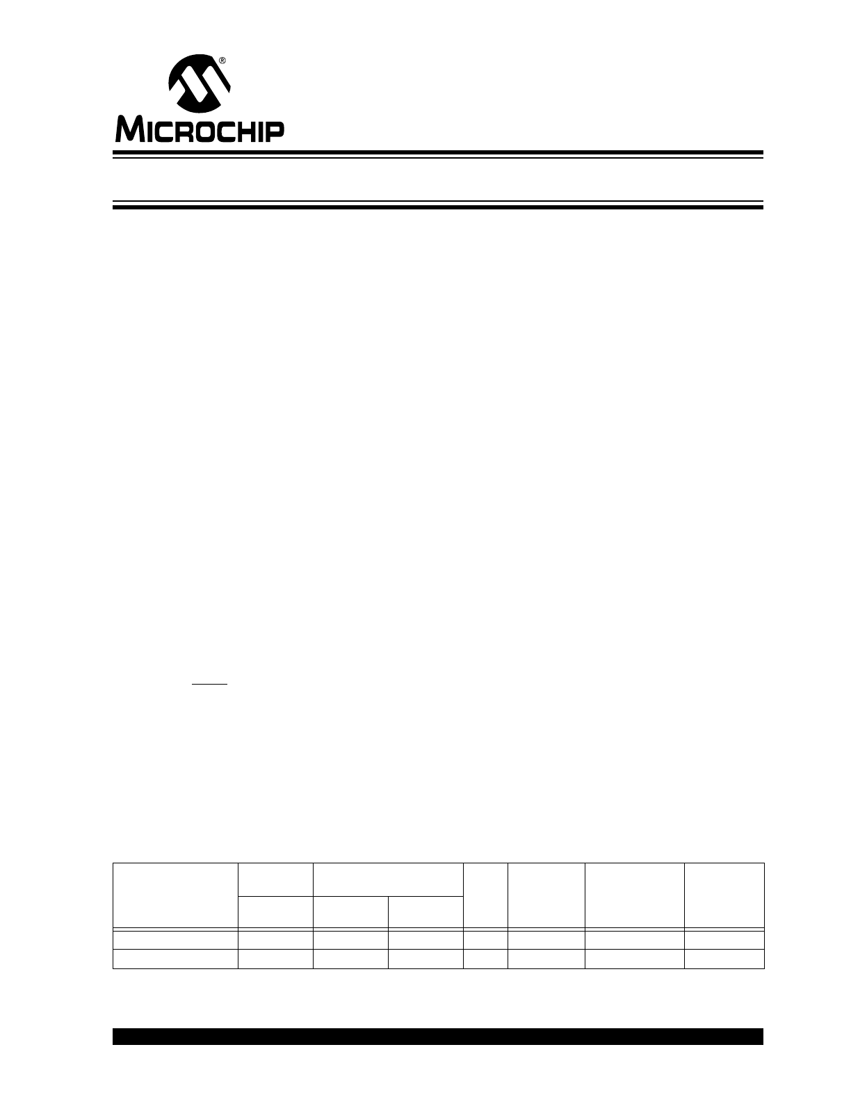
Pin Diagrams
V
SS
V
DD
GP5/T1CKI/OSC1/CLKIN
GP4/AN3/T1G/OSC2/CLKOUT
GP3/MCLR/V
PP
GP0/AN0/CIN+/ICSPDAT
GP1/AN1/CIN-/V
REF
/ICSPCLK
GP2/AN2/T0CKI/INT/COUT
1
2
3
4
5
6
7
8
PI
C
1
2F
675
V
SS
V
DD
GP5/T1CKI/OSC1/CLKIN
GP4/T1G/OSC2/CLKOUT
GP3/MCLR/V
PP
GP0/CIN+/ICSPDAT
GP1/CIN-/ICSPCLK
GP2/T0CKI/INT/COUT
1
2
3
4
5
6
7
8
P
IC
12F
629
8-pin PDIP, SOIC, DFN-S, DFN

2010 Microchip Technology Inc.
DS41190G-page 5
PIC12F629/675
Table of Contents
1.0
Device Overview ......................................................................................................................................................................... 7
2.0
Memory Organization.................................................................................................................................................................. 9
3.0
GPIO Port ................................................................................................................................................................................. 21
4.0
Timer0 Module .......................................................................................................................................................................... 29
5.0
Timer1 Module with Gate Control ............................................................................................................................................. 32
6.0
Comparator Module .................................................................................................................................................................. 37
7.0
Analog-to-Digital Converter (A/D) Module (PIC12F675 only) ................................................................................................... 43
8.0
Data EEPROM Memory ............................................................................................................................................................ 49
9.0
Special Features of the CPU .................................................................................................................................................... 53
10.0 Instruction Set Summary ........................................................................................................................................................... 71
11.0 Development Support ............................................................................................................................................................... 81
12.0 Electrical Specifications ............................................................................................................................................................ 85
13.0 DC and AC Characteristics Graphs and Tables ..................................................................................................................... 107
14.0 Packaging Information ............................................................................................................................................................ 117
Appendix A: Data Sheet Revision History ......................................................................................................................................... 127
Appendix B: Device Differences ....................................................................................................................................................... 127
Appendix C: Device Migrations ......................................................................................................................................................... 128
Appendix D: Migrating from other PIC
®
Devices .............................................................................................................................. 128
Index ................................................................................................................................................................................................. 129
On-Line Support ................................................................................................................................................................................ 133
Systems Information and Upgrade Hot Line ..................................................................................................................................... 133
Reader Response ............................................................................................................................................................................. 134
Product Identification System ........................................................................................................................................................... 135
TO OUR VALUED CUSTOMERS
It is our intention to provide our valued customers with the best documentation possible to ensure successful use of your Microchip
products. To this end, we will continue to improve our publications to better suit your needs. Our publications will be refined and
enhanced as new volumes and updates are introduced.
If you have any questions or comments regarding this publication, please contact the Marketing Communications Department via
E-mail at docerrors@microchip.com or fax the Reader Response Form in the back of this data sheet to (480) 792-4150. We
welcome your feedback.
Most Current Data Sheet
To obtain the most up-to-date version of this data sheet, please register at our Worldwide Web site at:
http://www.microchip.com
You can determine the version of a data sheet by examining its literature number found on the bottom outside corner of any page.
The last character of the literature number is the version number, (e.g., DS30000A is version A of document DS30000).
Errata
An errata sheet, describing minor operational differences from the data sheet and recommended workarounds, may exist for current
devices. As device/documentation issues become known to us, we will publish an errata sheet. The errata will specify the revision
of silicon and revision of document to which it applies.
To determine if an errata sheet exists for a particular device, please check with one of the following:
• Microchip’s Worldwide Web site; http://www.microchip.com
• Your local Microchip sales office (see last page)
When contacting a sales office, please specify which device, revision of silicon and data sheet (include literature number) you are
using.
Customer Notification System
Register on our web site at www.microchip.com to receive the most current information on all of our products.

PIC12F629/675
DS41190G-page 6
2010 Microchip Technology Inc.
NOTES:
2010 Microchip Technology Inc.
DS41190G-page 7
PIC12F629/675
1.0
DEVICE OVERVIEW
This document contains device specific information for
the PIC12F629/675. Additional information may be
found in the PIC
®
Mid-Range Reference Manual
(DS33023), which may be obtained from your local
Microchip Sales Representative or downloaded from
the Microchip web site. The Reference Manual should
be considered a complementary document to this Data
Sheet, and is highly recommended reading for a better
understanding of the device architecture and operation
of the peripheral modules.
The PIC12F629 and PIC12F675 devices are covered
by this Data Sheet. They are identical, except the
PIC12F675 has a 10-bit A/D converter. They come in
8-pin PDIP, SOIC, MLF-S and DFN packages.
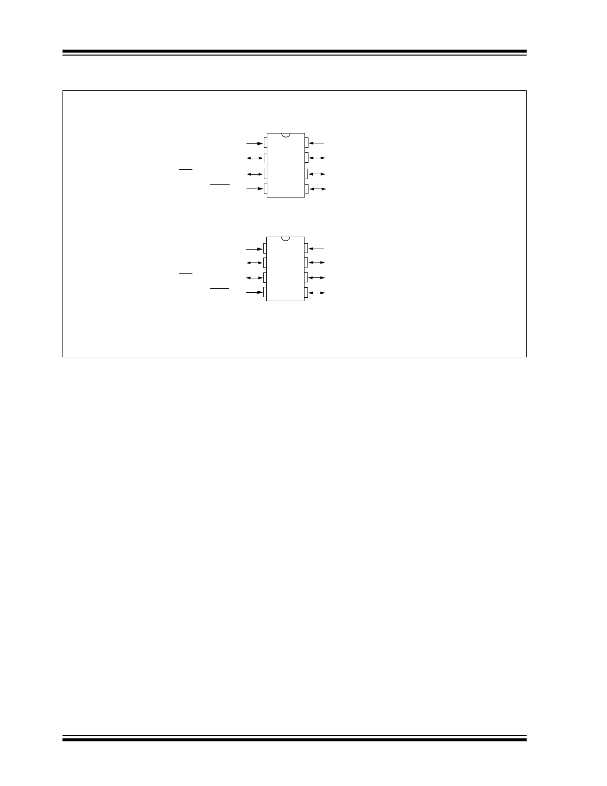
Figure 1-1 shows a block diagram of the PIC12F629/
675 devices. Table 1-1 shows the pinout description.
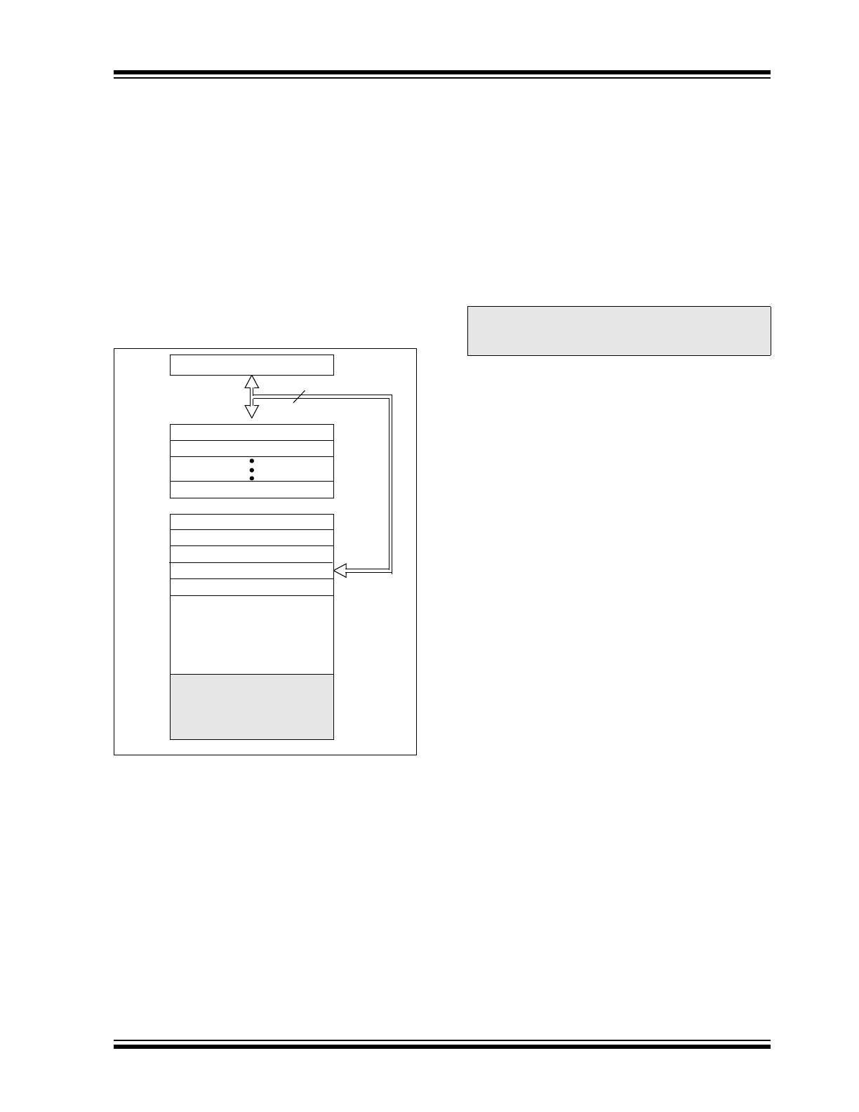
FIGURE 1-1:
PIC12F629/675 BLOCK DIAGRAM
Flash
Program
Memory
1K x 14
13
Data Bus
8
14
Program
Bus
Instruction Reg
Program Counter
8-Level Stack
(13-bit)
RAM
File
Registers
64 x 8
Direct Addr
7
Addr
(1)
9
Addr MUX
Indirect
Addr
FSR Reg
STATUS Reg
MUX
ALU
W Reg
Power-up
Timer
Oscillator
Start-up Timer
Power-on
Reset
Watchdog
Timer
Instruction
Decode &
Control
OSC1/CLKIN
OSC2/CLKOUT V
DD
, V
SS
8
8
Brown-out
Detect
8
3
Timing
Generation
GP5/T1CKI/OSC1/CLKIN
Internal
4 MHz
RAM
GP4/AN3/T1G/OSC2/CLKOUT
GP3/MCLR/V
PP
GP2/AN2/T0CKI/INT/COUT
GP1/AN1/CIN-/V
REF
GP0/AN0/CIN+
Oscillator
Note 1: Higher order bits are from STATUS register.
Analog
Timer0
Timer1
DATA
EEPROM
128 bytes
EEDATA
EEADDR
Comparator
Analog to Digital Converter
(PIC12F675 only)
AN0 AN1 AN2 AN3
CIN- CIN+ COUT
T0CKI
T1CKI
V
REF
and reference
T1G
8
PIC12F629/675
DS41190G-page 8
2010 Microchip Technology Inc.
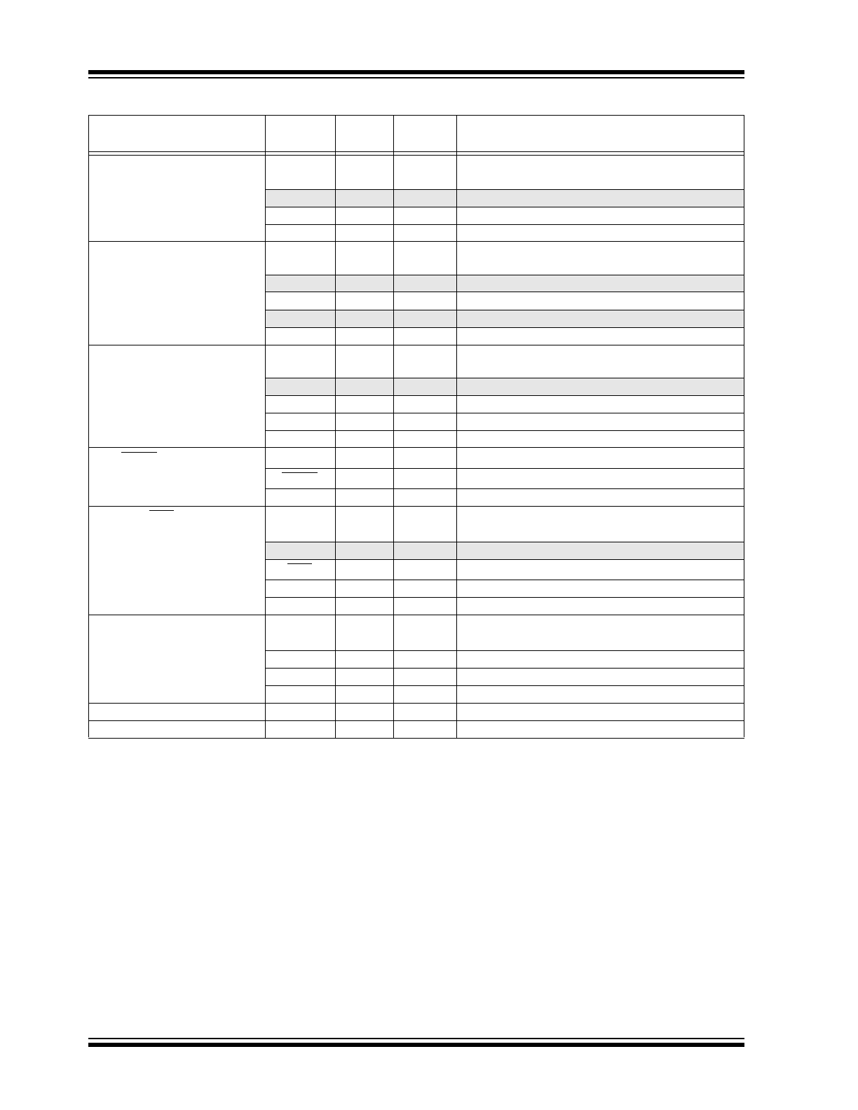
TABLE 1-1:
PIC12F629/675 PINOUT DESCRIPTION
Name
Function
Input
Type
Output
Type
Description
GP0/AN0/CIN+/ICSPDAT
GP0
TTL
CMOS
Bidirectional I/O w/ programmable pull-up and
interrupt-on-change
AN0
AN
A/D Channel 0 input
CIN+
AN
Comparator input
ICSPDAT
TTL
CMOS
Serial programming I/O
GP1/AN1/CIN-/V
REF
/
ICSPCLK
GP1
TTL
CMOS
Bidirectional I/O w/ programmable pull-up and
interrupt-on-change
AN1
AN
A/D Channel 1 input
CIN-
AN
Comparator input
V
REF
AN
External voltage reference
ICSPCLK
ST
Serial programming clock
GP2/AN2/T0CKI/INT/COUT
GP2
ST
CMOS
Bidirectional I/O w/ programmable pull-up and
interrupt-on-change
AN2
AN
A/D Channel 2 input
T0CKI
ST
TMR0 clock input
INT
ST
External interrupt
COUT
CMOS
Comparator output
GP3/MCLR/V
PP
GP3
TTL
Input port w/ interrupt-on-change
MCLR
ST
Master Clear
V
PP
HV
Programming voltage
GP4/AN3/T1G/OSC2/
CLKOUT
GP4
TTL
CMOS
Bidirectional I/O w/ programmable pull-up and
interrupt-on-change
AN3
AN
A/D Channel 3 input
T1G
ST
TMR1 gate
OSC2
XTAL
Crystal/resonator
CLKOUT
CMOS
F
OSC
/4 output
GP5/T1CKI/OSC1/CLKIN
GP5
TTL
CMOS
Bidirectional I/O w/ programmable pull-up and
interrupt-on-change
T1CKI
ST
TMR1 clock
OSC1
XTAL
Crystal/resonator
CLKIN
ST
External clock input/RC oscillator connection
V
SS
V
SS
Power
Ground reference
V
DD
V
DD
Power
Positive supply
Legend: Shade = PIC12F675 only
TTL = TTL input buffer, ST = Schmitt Trigger input buffer
2010 Microchip Technology Inc.
DS41190G-page 9
PIC12F629/675
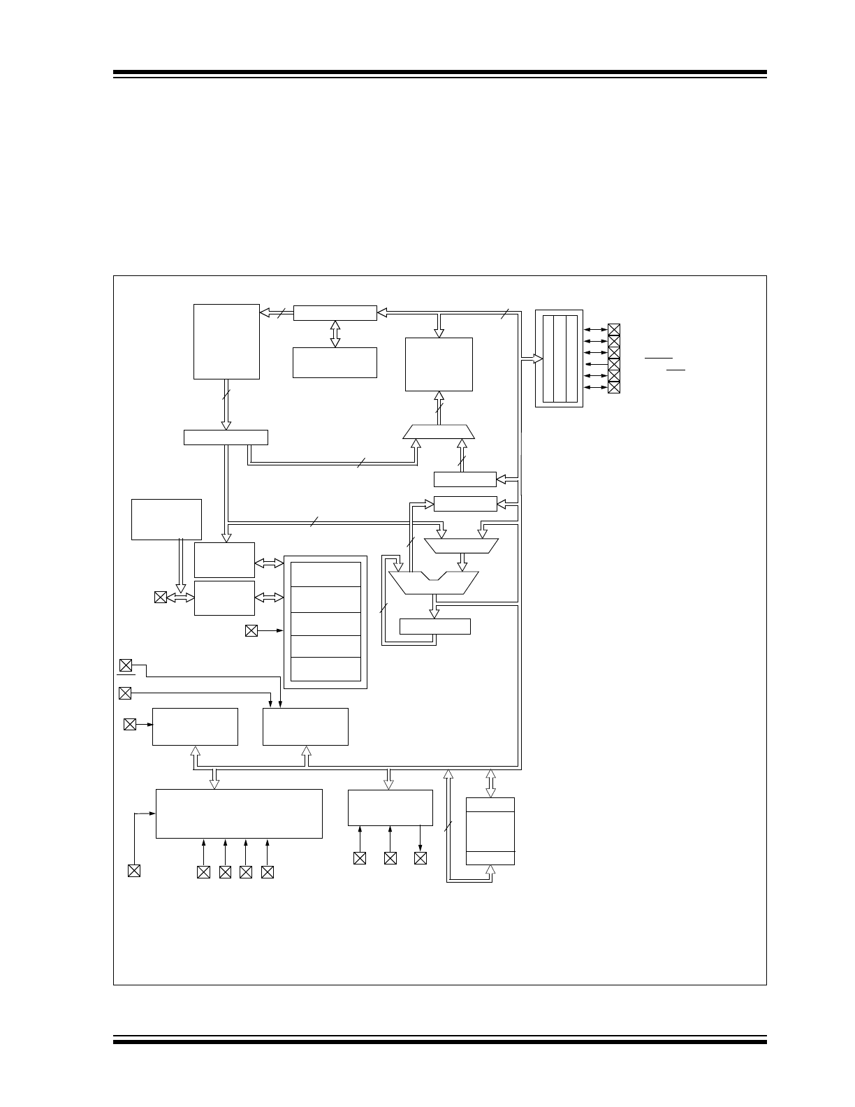
2.0
MEMORY ORGANIZATION
2.1
Program Memory Organization
The PIC12F629/675 devices have a 13-bit program
counter capable of addressing an 8K x 14 program
memory space. Only the first 1K x 14 (0000h-03FFh)
for the PIC12F629/675 devices is physically imple-
mented. Accessing a location above these boundaries
will cause a wrap-around within the first 1K x 14 space.
The Reset vector is at 0000h and the interrupt vector is
at 0004h (see Figure 2-1).
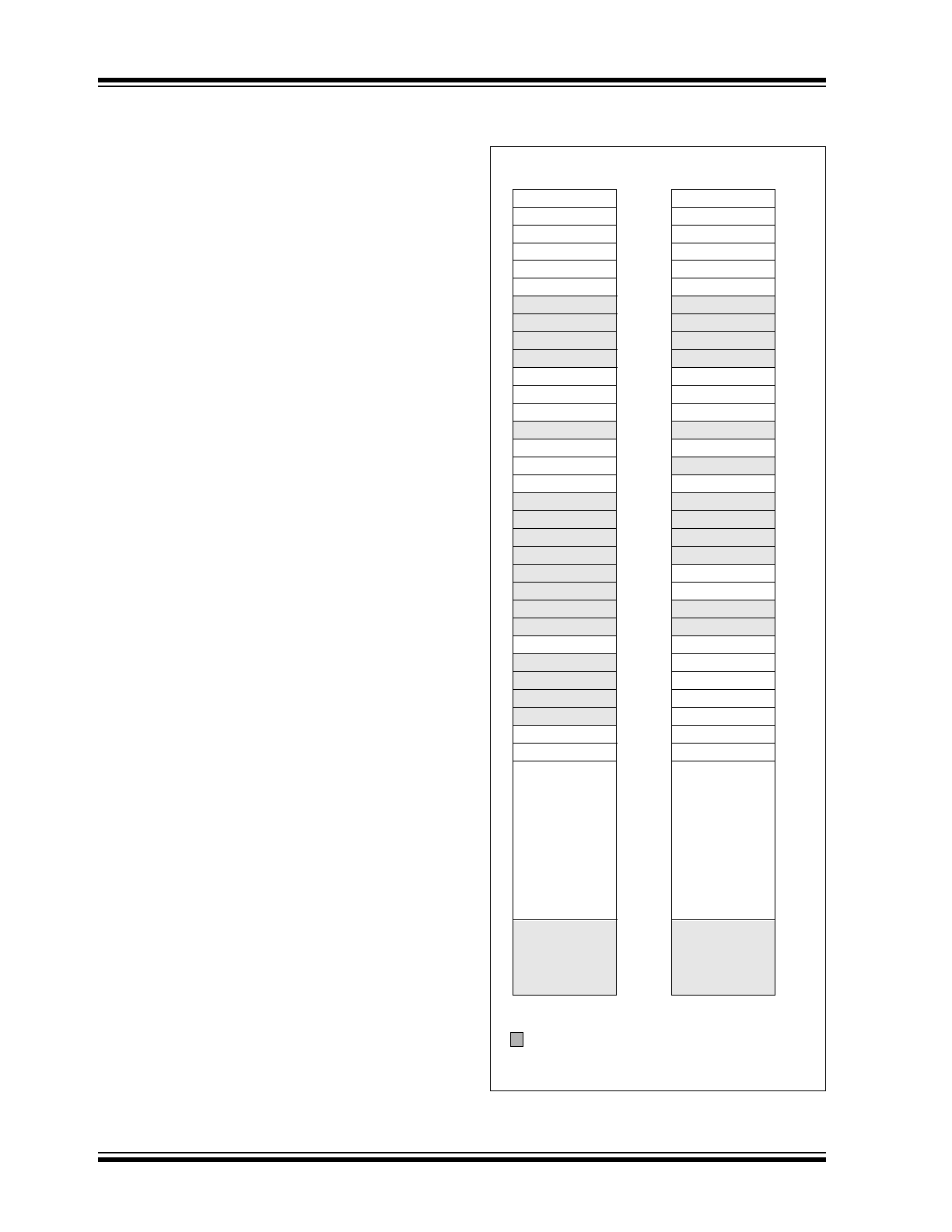
FIGURE 2-1:
PROGRAM MEMORY MAP
AND STACK FOR THE
DSTEMP/675
2.2
Data Memory Organization
The data memory (see Figure 2-2) is partitioned into
two banks, which contain the General Purpose
Registers and the Special Function Registers. The
Special Function Registers are located in the first 32
locations of each bank. Register locations 20h-5Fh are
General Purpose Registers, implemented as static
RAM and are mapped across both banks. All other
RAM is unimplemented and returns ‘0’ when read. RP0
(STATUS<5>) is the bank select bit.
• RP0 = 0 Bank 0 is selected
• RP0 = 1 Bank 1 is selected
2.2.1
GENERAL PURPOSE REGISTER
FILE
The register file is organized as 64 x 8 in the
PIC12F629/675 devices. Each register is accessed,
either directly or indirectly, through the File Select
Register FSR (see Section 2.4 “Indirect Addressing,
INDF and FSR Registers”).
PC<12:0>
13
000h
0004
0005
03FFh
0400h
1FFFh
Stack Level 1
Stack Level 8
Reset Vector
Interrupt Vector
On-chip Program
Memory
CALL, RETURN
RETFIE, RETLW
Stack Level 2
Note:
The IRP and RP1 bits STATUS<7:6> are
reserved and should always be maintained
as ‘0’s.
PIC12F629/675
DS41190G-page 10
2010 Microchip Technology Inc.
2.2.2
SPECIAL FUNCTION REGISTERS
The Special Function Registers are registers used by
the CPU and peripheral functions for controlling the
desired operation of the device (see Table 2-1). These
registers are static RAM.
The special registers can be classified into two sets:
core and peripheral. The Special Function Registers
associated with the “core” are described in this section.
Those related to the operation of the peripheral
features are described in the section of that peripheral
feature.
FIGURE 2-2:
DATA MEMORY MAP OF
THE PIC12F629/675
Indirect addr.
(1)
TMR0
PCL
STATUS
FSR
GPIO
PCLATH
INTCON
PIR1
TMR1L
TMR1H
T1CON
00h
01h
02h
03h
04h
05h
06h
07h
08h
09h
0Ah
0Bh
0Ch
0Dh
0Eh
0Fh
10h
11h
12h
13h
14h
15h
16h
17h
18h
19h
1Ah
1Bh
1Ch
1Dh
1Eh
1Fh
20h
7Fh
Bank 0
Unimplemented data memory locations, read as ‘
0
’.
1: Not a physical register.
2: PIC12F675 only.
CMCON
VRCON
General
Purpose
Registers
accesses
20h-5Fh
64 Bytes
EEDATA
EEADR
EECON2
(1)
5Fh
60h
File
Address
File
Address
WPU
IOC
Indirect addr.
(1)
OPTION_REG
PCL
STATUS
FSR
TRISIO
PCLATH
INTCON
PIE1
PCON
OSCCAL
80h
81h
82h
83h
84h
85h
86h
87h
88h
89h
8Ah
8Bh
8Ch
8Dh
8Eh
8Fh
90h
91h
92h
93h
94h
95h
96h
97h
98h
99h
9Ah
9Bh
9Ch
9Dh
9Eh
9Fh
A0h
FFh
Bank 1
DFh
E0h
ADRESH
(2)
ADCON0
(2)
EECON1
ADRESL
(2)
ANSEL
(2)