

2010 Microchip Technology Inc.
DS41302D
PIC12F609/615/617
PIC12HV609/615
Data Sheet
8-Pin, Flash-Based 8-Bit
CMOS Microcontrollers
*8-bit, 8-pin Devices Protected by Microchip’s Low Pin Count Patent: U.S. Patent No. 5,847,450. Additional U.S. and
foreign patents and applications may be issued or pending.
DS41302D-page 2
2010 Microchip Technology Inc.
Information contained in this publication regarding device
applications and the like is provided only for your convenience
and may be superseded by updates. It is your responsibility to
ensure that your application meets with your specifications.
MICROCHIP MAKES NO REPRESENTATIONS OR
WARRANTIES OF ANY KIND WHETHER EXPRESS OR
IMPLIED, WRITTEN OR ORAL, STATUTORY OR
OTHERWISE, RELATED TO THE INFORMATION,
INCLUDING BUT NOT LIMITED TO ITS CONDITION,
QUALITY, PERFORMANCE, MERCHANTABILITY OR
FITNESS FOR PURPOSE. Microchip disclaims all liability
arising from this information and its use. Use of Microchip
devices in life support and/or safety applications is entirely at
the buyer’s risk, and the buyer agrees to defend, indemnify and
hold harmless Microchip from any and all damages, claims,
suits, or expenses resulting from such use. No licenses are
conveyed, implicitly or otherwise, under any Microchip
intellectual property rights.
Trademarks
The Microchip name and logo, the Microchip logo, dsPIC,
K
EE
L
OQ
, K
EE
L
OQ
logo, MPLAB, PIC, PICmicro, PICSTART,
rfPIC and UNI/O are registered trademarks of Microchip
Technology Incorporated in the U.S.A. and other countries.
FilterLab, Hampshire, HI-TECH C, Linear Active Thermistor,
MXDEV, MXLAB, SEEVAL and The Embedded Control
Solutions Company are registered trademarks of Microchip
Technology Incorporated in the U.S.A.
Analog-for-the-Digital Age, Application Maestro, CodeGuard,
dsPICDEM, dsPICDEM.net, dsPICworks, dsSPEAK, ECAN,
ECONOMONITOR, FanSense, HI-TIDE, In-Circuit Serial
Programming, ICSP, Mindi, MiWi, MPASM, MPLAB Certified
logo, MPLIB, MPLINK, mTouch, Octopus, Omniscient Code
Generation, PICC, PICC-18, PICDEM, PICDEM.net, PICkit,
PICtail, PIC
32
logo, REAL ICE, rfLAB, Select Mode, Total
Endurance, TSHARC, UniWinDriver, WiperLock and ZENA
are trademarks of Microchip Technology Incorporated in the
U.S.A. and other countries.
SQTP is a service mark of Microchip Technology Incorporated
in the U.S.A.
All other trademarks mentioned herein are property of their
respective companies.
© 2010, Microchip Technology Incorporated, Printed in the
U.S.A., All Rights Reserved.
Printed on recycled paper.
Note the following details of the code protection feature on Microchip devices:
•
Microchip products meet the specification contained in their particular Microchip Data Sheet.
•
Microchip believes that its family of products is one of the most secure families of its kind on the market today, when used in the
intended manner and under normal conditions.
•
There are dishonest and possibly illegal methods used to breach the code protection feature. All of these methods, to our
knowledge, require using the Microchip products in a manner outside the operating specifications contained in Microchip’s Data
Sheets. Most likely, the person doing so is engaged in theft of intellectual property.
•
Microchip is willing to work with the customer who is concerned about the integrity of their code.
•
Neither Microchip nor any other semiconductor manufacturer can guarantee the security of their code. Code protection does not
mean that we are guaranteeing the product as “unbreakable.”
Code protection is constantly evolving. We at Microchip are committed to continuously improving the code protection features of our
products. Attempts to break Microchip’s code protection feature may be a violation of the Digital Millennium Copyright Act. If such acts
allow unauthorized access to your software or other copyrighted work, you may have a right to sue for relief under that Act.
Microchip received ISO/TS-16949:2002 certification for its worldwide
headquarters, design and wafer fabrication facilities in Chandler and
Tempe, Arizona; Gresham, Oregon and design centers in California
and India. The Company’s quality system processes and procedures
are for its PIC
®
MCUs and dsPIC
®
DSCs, K
EE
L
OQ
®
code hopping
devices, Serial EEPROMs, microperipherals, nonvolatile memory and
analog products. In addition, Microchip’s quality system for the design
and manufacture of development systems is ISO 9001:2000 certified.

2010 Microchip Technology Inc.
DS41302D-page 3
PIC12F609/615/617/12HV609/615
High-Performance RISC CPU:
• Only 35 Instructions to Learn:
- All single-cycle instructions except branches
• Operating Speed:
- DC – 20 MHz oscillator/clock input
- DC – 200 ns instruction cycle
• Interrupt Capability
• 8-Level Deep Hardware Stack
• Direct, Indirect and Relative Addressing modes
Special Microcontroller Features:
• Precision Internal Oscillator:
- Factory calibrated to ±1%, typical
- Software selectable frequency: 4 MHz or
8 MHz
• Power-Saving Sleep mode
• Voltage Range:
- PIC12F609/615/617: 2.0V to 5.5V
- PIC12HV609/615: 2.0V to user defined
maximum (see note)
• Industrial and Extended Temperature Range
• Power-on Reset (POR)
• Power-up Timer (PWRT) and Oscillator Start-up
Timer (OST)
• Brown-out Reset (BOR)
• Watchdog Timer (WDT) with independent
Oscillator for Reliable Operation
• Multiplexed Master Clear with Pull-up/Input Pin
• Programmable Code Protection
• High Endurance Flash:
- 100,000 write Flash endurance
- Flash retention: > 40 years
• Self Read/ Write Program Memory (PIC12F617
only)
Low-Power Features:
• Standby Current:
- 50 nA @ 2.0V, typical
• Operating Current:
- 11
A @ 32 kHz, 2.0V, typical
- 260
A @ 4 MHz, 2.0V, typical
• Watchdog Timer Current:
- 1
A @ 2.0V, typical
Note:
Voltage across the shunt regulator should
not exceed 5V.
Peripheral Features:
• Shunt Voltage Regulator (PIC12HV609/615 only):
- 5 volt regulation
- 4 mA to 50 mA shunt range
• 5 I/O Pins and 1 Input Only
• High Current Source/Sink for Direct LED Drive
- Interrupt-on-pin change or pins
- Individually programmable weak pull-ups
• Analog Comparator module with:
- One analog comparator
- Programmable on-chip voltage reference
(CV
REF
) module (% of V
DD
)
- Comparator inputs and output externally
accessible
- Built-In Hysteresis (software selectable)
• Timer0: 8-Bit Timer/Counter with 8-Bit
Programmable Prescaler
• Enhanced Timer1:
- 16-bit timer/counter with prescaler
- External Timer1 Gate (count enable)
- Option to use OSC1 and OSC2 in LP mode
as Timer1 oscillator if INTOSC mode
selected
- Option to use system clock as Timer1
• In-Circuit Serial Programming
TM
(ICSP
TM
) via Two
Pins
PIC12F615/617/HV615 ONLY:
• Enhanced Capture, Compare, PWM module:
- 16-bit Capture, max. resolution 12.5 ns
- Compare, max. resolution 200 ns
- 10-bit PWM with 1 or 2 output channels, 1
output channel programmable “dead time,”
max. frequency 20 kHz, auto-shutdown
• A/D Converter:
- 10-bit resolution and 4 channels, samples
internal voltage references
• Timer2: 8-Bit Timer/Counter with 8-Bit Period
Register, Prescaler and Postscaler
8-Pin Flash-Based, 8-Bit CMOS Microcontrollers
PIC12F609/615/617/12HV609/615
DS41302D-page 4
2010 Microchip Technology Inc.
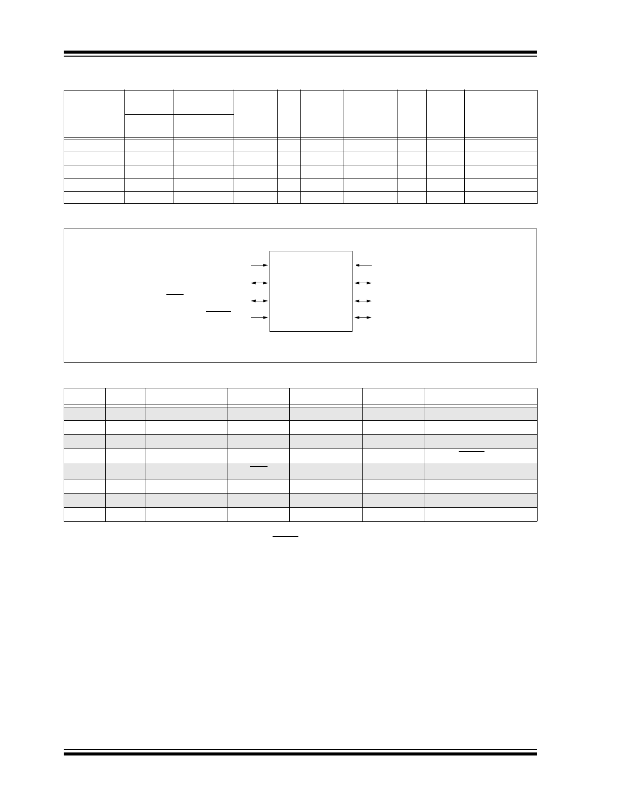
8-Pin Diagram, PIC12F609/HV609 (PDIP, SOIC, MSOP, DFN)
TABLE 1:
PIC12F609/HV609 PIN SUMMARY (
PDIP, SOIC, MSOP, DFN
)
Device
Program
Memory
Data Memory
Self Read/
Self Write
I/O
10-bit A/D
(ch)
Comparators ECCP
Timers
8/16-bit
Voltage Range
Flash
(words)
SRAM (bytes)
PIC12F609
1024
64
—
5
0
1
—
1/1
2.0V-5.5V
PIC12HV609
1024
64
—
5
0
1
—
1/1
2.0V-user defined
PIC12F615
1024
64
—
5
4
1
YES
2/1
2.0V-5.5V
PIC12HV615
1024
64
—
5
4
1
YES
2/1
2.0V-user defined
PIC12F617
2048
128
YES
5
4
1
YES
2/1
2.0V-5.5V
I/O
Pin
Comparators
Timer
Interrupts
Pull-ups
Basic
GP0
7
CIN+
—
IOC
Y
ICSPDAT
GP1
6
CIN0-
—
IOC
Y
ICSPCLK
GP2
5
COUT
T0CKI
INT/IOC
Y
—
GP3
(1)
4
—
—
IOC
Y
(2)
MCLR/V
PP
GP4
3
CIN1-
T1G
IOC
Y
OSC2/CLKOUT
GP5
2
—
T1CKI
IOC
Y
OSC1/CLKIN
—
1
—
—
—
—
V
DD
—
8
—
—
—
—
V
SS
Note 1:
Input only.
2:
Only when pin is configured for external MCLR.
1
2
3
4
5
6
7
8
PIC12F609/
HV609
V
SS
GP0/CIN+/ICSPDAT
GP1/CIN0-/ICSPCLK
GP2/T0CKI/INT/COUT
V
DD
GP5/T1CKI/OSC1/CLKIN
GP4/CIN1-/T1G/OSC2/CLKOUT
GP3/MCLR/V
PP
2010 Microchip Technology Inc.
DS41302D-page 5
PIC12F609/615/617/12HV609/615
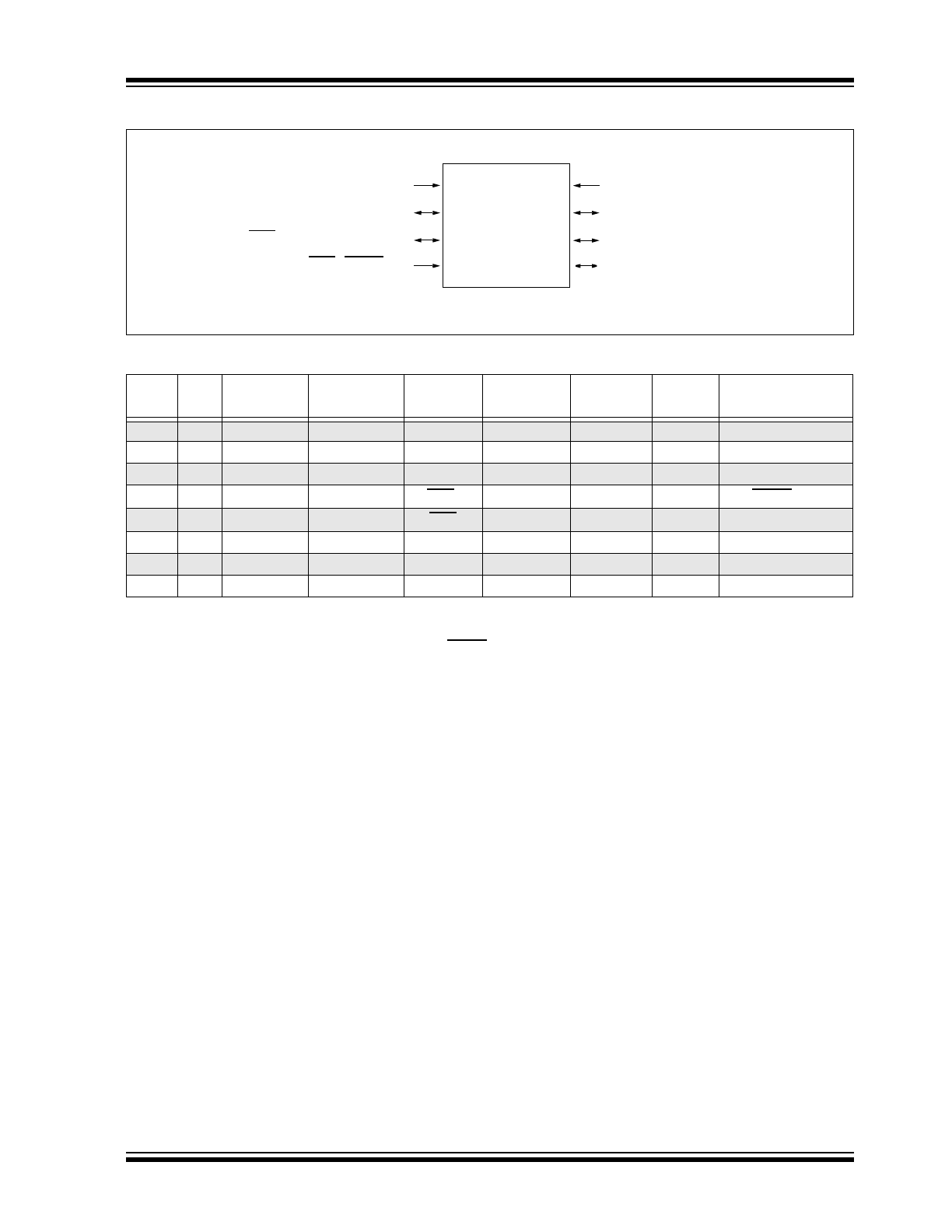
8-Pin Diagram, PIC12F615/617/HV615 (PDIP, SOIC, MSOP, DFN)
TABLE 2:
PIC12F615/617/HV615 PIN SUMMARY (
PDIP, SOIC, MSOP, DFN
)
I/O
Pin
Analog
Comparator
s
Timer
CCP
Interrupts
Pull-ups
Basic
GP0
7
AN0
CIN+
—
P1B
IOC
Y
ICSPDAT
GP1
6
AN1
CIN0-
—
—
IOC
Y
ICSPCLK/V
REF
GP2
5
AN2
COUT
T0CKI
CCP1/P1A
INT/IOC
Y
—
GP3
(1)
4
—
—
T1G*
—
IOC
Y
(2)
MCLR/V
PP
GP4
3
AN3
CIN1-
T1G
P1B*
IOC
Y
OSC2/CLKOUT
GP5
2
—
—
T1CKI
P1A*
IOC
Y
OSC1/CLKIN
—
1
—
—
—
—
—
—
V
DD
—
8
—
—
—
—
—
—
V
SS
*
Alternate pin function.
Note 1:
Input only.
2:
Only when pin is configured for external MCLR.
1
2
3
4
5
6
7
8
PIC12F615/
617/HV615
V
SS
GP0/AN0/CIN+/P1B/ICSPDAT
GP1/AN1/CIN0-/V
REF
/ICSPCLK
GP2/AN2/T0CKI/INT/COUT/CCP1/P1A
V
DD
GP5/T1CKI/P1A*/OSC1/CLKIN
GP4/AN3/CIN1-/T1G/P1B*/OSC2/CLKOUT
GP3/T1G*/MCLR/V
PP
*
Alternate pin function.

PIC12F609/615/617/12HV609/615
DS41302D-page 6
2010 Microchip Technology Inc.
Table of Contents
1.0
Device Overview ......................................................................................................................................................................... 7
2.0
Memory Organization ................................................................................................................................................................ 11
3.0
Flash Program Memory Self Read/Self Write Control (PIC12F617 only).................................................................................. 27
4.0
Oscillator Module ....................................................................................................................................................................... 37
5.0 I/O
Port
...................................................................................................................................................................................... 43
6.0 Timer0
Module
.......................................................................................................................................................................... 53
7.0
Timer1 Module with Gate Control .............................................................................................................................................. 57
8.0
Timer2 Module (PIC12F615/617/HV615 only) .......................................................................................................................... 65
9.0 Comparator
Module
................................................................................................................................................................... 67
10.0 Analog-to-Digital Converter (ADC) Module (PIC12F615/617/HV615 only) ............................................................................... 79
11.0 Enhanced Capture/Compare/PWM (With Auto-Shutdown and Dead Band) Module (PIC12F615/617/HV615 only) ............... 89
12.0 Special Features of the CPU ................................................................................................................................................... 107
13.0 Voltage
Regulator .................................................................................................................................................................... 127
14.0 Instruction Set Summary ........................................................................................................................................................ 129
15.0 Development Support ............................................................................................................................................................. 139
16.0 Electrical Specifications ........................................................................................................................................................... 143
17.0 DC and AC Characteristics Graphs and Tables ...................................................................................................................... 171
18.0 Packaging Information ............................................................................................................................................................ 195
Appendix A: Data Sheet Revision History ......................................................................................................................................... 203
Appendix B: Migrating from other PIC
®
Devices ............................................................................................................................... 203
Index ................................................................................................................................................................................................. 205
The Microchip Web Site .................................................................................................................................................................... 209
Customer Change Notification Service ............................................................................................................................................. 209
Customer Support ............................................................................................................................................................................. 209
Reader Response ............................................................................................................................................................................. 210
Product Identification System ............................................................................................................................................................ 211
Worldwide Sales and Service ........................................................................................................................................................... 212
TO OUR VALUED CUSTOMERS
It is our intention to provide our valued customers with the best documentation possible to ensure successful use of your Microchip
products. To this end, we will continue to improve our publications to better suit your needs. Our publications will be refined and
enhanced as new volumes and updates are introduced.
If you have any questions or comments regarding this publication, please contact the Marketing Communications Department via
E-mail at docerrors@microchip.com or fax the Reader Response Form in the back of this data sheet to (480) 792-4150. We
welcome your feedback.
Most Current Data Sheet
To obtain the most up-to-date version of this data sheet, please register at our Worldwide Web site at:
http://www.microchip.com
You can determine the version of a data sheet by examining its literature number found on the bottom outside corner of any page.
The last character of the literature number is the version number, (e.g., DS30000A is version A of document DS30000).
Errata
An errata sheet, describing minor operational differences from the data sheet and recommended workarounds, may exist for current
devices. As device/documentation issues become known to us, we will publish an errata sheet. The errata will specify the revision of
silicon and revision of document to which it applies.
To determine if an errata sheet exists for a particular device, please check with one of the following:
• Microchip’s Worldwide Web site; http://www.microchip.com
• Your local Microchip sales office (see last page)
When contacting a sales office, please specify which device, revision of silicon and data sheet (include literature number) you are
using.
Customer Notification System
Register on our web site at www.microchip.com to receive the most current information on all of our products.
2010 Microchip Technology Inc.
DS41302D-page 7
PIC12F609/615/617/12HV609/615
1.0
DEVICE OVERVIEW
The PIC12F609/615/617/12HV609/615 devices are
covered by this data sheet. They are available in 8-pin
PDIP, SOIC, MSOP and DFN packages.
Block Diagrams and pinout descriptions of the devices
are as follows:
• PIC12F609/HV609 (Figure 1-1, Table 1-1)
• PIC12F615/617/HV615 (Figure 1-2, Table 1-2)
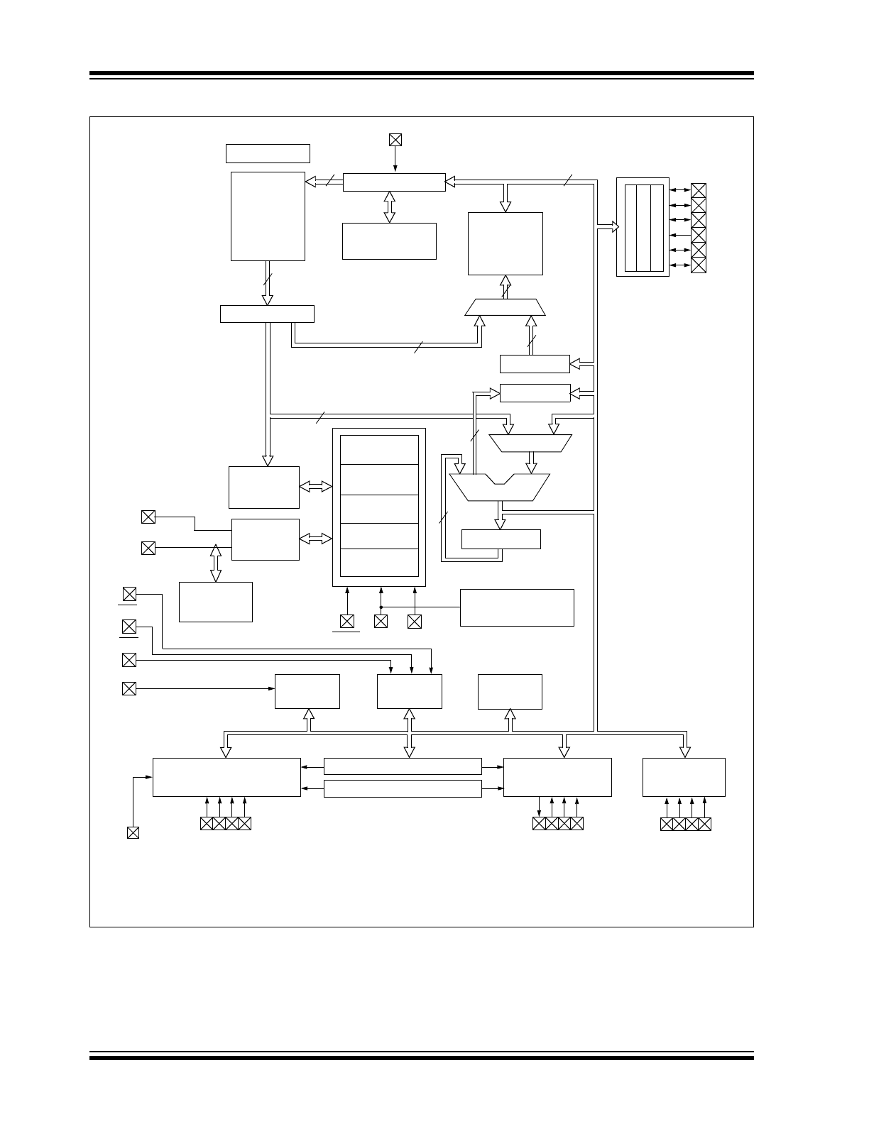
FIGURE 1-1:
PIC12F609/HV609 BLOCK DIAGRAM
Flash
Program
Memory
13
Data Bus
8
14
Program
Bus
Instruction Reg
Program Counter
RAM
File
Registers
Direct Addr
7
RAM Addr
9
Addr MUX
Indirect
Addr
FSR Reg
STATUS Reg
MUX
ALU
W Reg
Instruction
Decode &
Control
Timing
Generation
OSC1/CLKIN
OSC2/CLKOUT
GPIO
8
8
8
3
8-Level Stack
64 Bytes
1K X 14
(13-Bit)
Power-up
Timer
Oscillator
Start-up Timer
Power-on
Reset
Watchdog
Timer
MCLR
V
SS
Brown-out
Reset
Timer0
Timer1
GP0
GP1
GP2
GP3
GP4
GP5
Analog Comparator
T0CKI
INT
T1CKI
Configuration
Internal
Oscillator
and Reference
T1G
V
DD
Block
CI
N+
CI
N0
-
CI
N1
-
CO
UT
Comparator Voltage Reference
Absolute Voltage Reference
Shunt Regulator
(PIC12HV609 only)
PIC12F609/615/617/12HV609/615
DS41302D-page 8
2010 Microchip Technology Inc.
FIGURE 1-2:
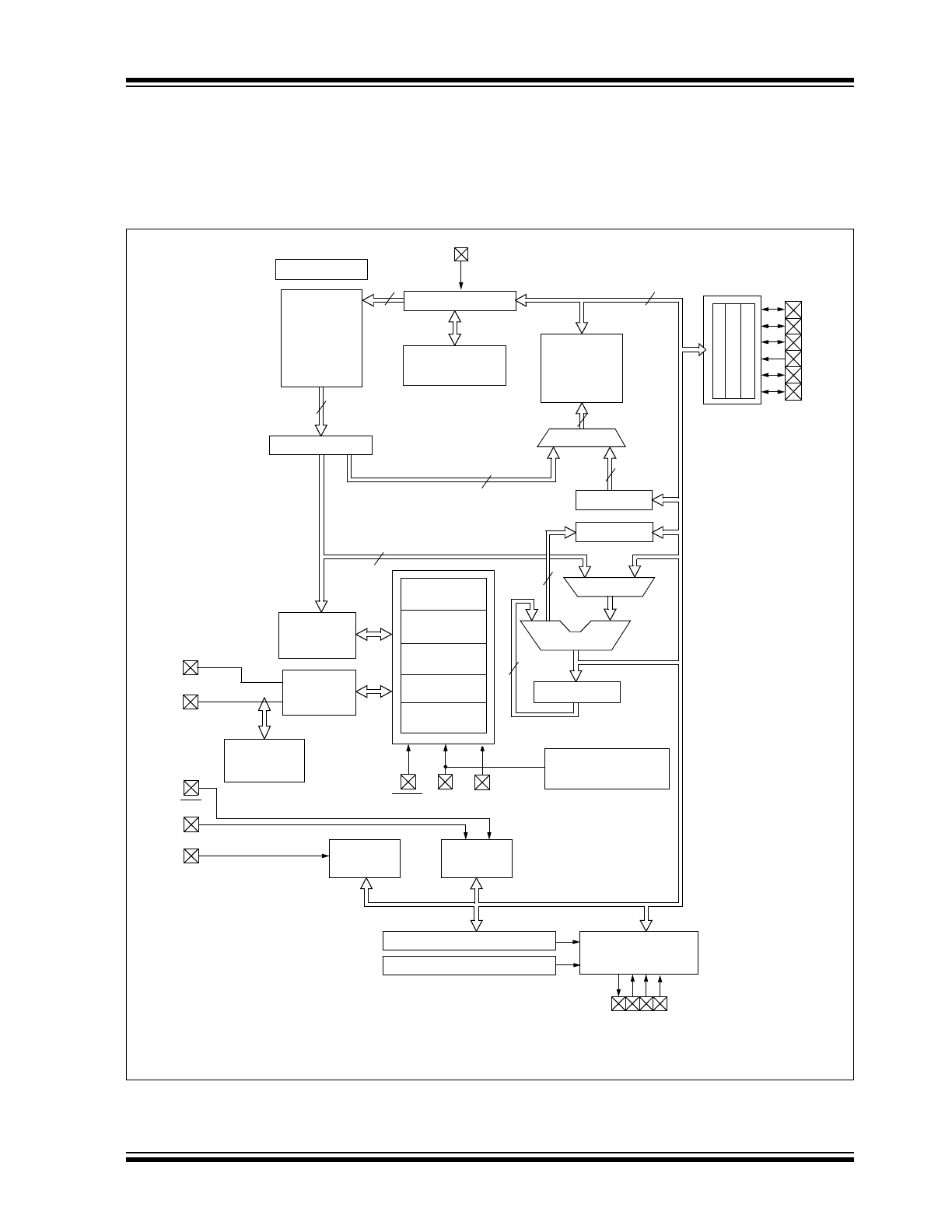
PIC12F615/617/HV615 BLOCK DIAGRAM
Flash
Program
Memory
13
Data Bus
8
14
Program
Bus
Instruction Reg
Program Counter
RAM
File
Registers
Direct Addr
7
RAM Addr
9
Addr MUX
Indirect
Addr
FSR Reg
STATUS Reg
MUX
ALU
W Reg
Instruction
Decode &
Control
Timing
Generation
OSC1/CLKIN
OSC2/CLKOUT
GPIO
8
8
8
3
8-Level Stack
64 Bytes and
1K X 14
(13-Bit)
Power-up
Timer
Oscillator
Start-up Timer
Power-on
Reset
Watchdog
Timer
MCLR
V
SS
Brown-out
Reset
Timer0
Timer1
GP0
GP1
GP2
GP3
GP4
GP5
Analog Comparator
T0CKI
INT
T1CKI
Configuration
Internal
Oscillator
V
RE
F
and Reference
T1G
V
DD
Timer2
Block
Shunt Regulator
(PIC12HV615 only)
Analog-To-Digital Converter
AN0
AN1
AN2
AN3
CIN+
CIN0
-
CIN1
-
COUT
ECCP
CCP1
/P1
A
P1
B
P1
A*
P1
B*
Comparator Voltage Reference
Absolute Voltage Reference
*
Alternate pin function.
**
For the PIC12F617 only.
T1G*
2K X 14**
and
128 Bytes**
2010 Microchip Technology Inc.
DS41302D-page 9
PIC12F609/615/617/12HV609/615
TABLE 1-1:
PIC12F609/HV609 PINOUT DESCRIPTION
Name
Function
Input
Type
Output
Type
Description
GP0/CIN+/ICSPDAT
GP0
TTL
CMOS
General purpose I/O with prog. pull-up and interrupt-on-change
CIN+
AN
—
Comparator non-inverting input
ICSPDAT
ST
CMOS
Serial Programming Data I/O
GP1/CIN0-/ICSPCLK
GP1
TTL
CMOS
General purpose I/O with prog. pull-up and interrupt-on-change
CIN0-
AN
—
Comparator inverting input
ICSPCLK
ST
—
Serial Programming Clock
GP2/T0CKI/INT/COUT
GP2
ST
CMOS
General purpose I/O with prog. pull-up and interrupt-on-change
T0CKI
ST
—
Timer0 clock input
INT
ST
—
External Interrupt
COUT
—
CMOS
Comparator output
GP3/MCLR/V
PP
GP3
TTL
—
General purpose input with interrupt-on-change
MCLR
ST
—
Master Clear w/internal pull-up
V
PP
HV
—
Programming voltage
GP4/CIN1-/T1G/OSC2/
CLKOUT
GP4
TTL
CMOS
General purpose I/O with prog. pull-up and interrupt-on-change
CIN1-
AN
—
Comparator inverting input
T1G
ST
—
Timer1 gate (count enable)
OSC2
—
XTAL
Crystal/Resonator
CLKOUT
—
CMOS
F
OSC
/4 output
GP5/T1CKI/OSC1/CLKIN
GP5
TTL
CMOS
General purpose I/O with prog. pull-up and interrupt-on-change
T1CKI
ST
—
Timer1 clock input
OSC1
XTAL
—
Crystal/Resonator
CLKIN
ST
—
External clock input/RC oscillator connection
V
DD
V
DD
Power
—
Positive supply
V
SS
V
SS
Power
—
Ground reference
Legend: AN=Analog input or output
CMOS = CMOS compatible input or output
HV=
High Voltage
ST=Schmitt Trigger input with CMOS levels
TTL
= TTL compatible input
XTAL=Crystal
PIC12F609/615/617/12HV609/615
DS41302D-page 10
2010 Microchip Technology Inc.
TABLE 1-2:
PIC12F615/617/HV615 PINOUT DESCRIPTION
Name
Function
Input
Type
Output
Type
Description
GP0/AN0/CIN+/P1B/ICSPDAT
GP0
TTL
CMOS
General purpose I/O with prog. pull-up and interrupt-on-
change
AN0
AN
—
A/D Channel 0 input
CIN+
AN
—
Comparator non-inverting input
P1B
—
CMOS
PWM output
ICSPDAT
ST
CMOS
Serial Programming Data I/O
GP1/AN1/CIN0-/V
REF
/ICSPCLK
GP1
TTL
CMOS
General purpose I/O with prog. pull-up and interrupt-on-
change
AN1
AN
—
A/D Channel 1 input
CIN0-
AN
—
Comparator inverting input
V
REF
AN
—
External Voltage Reference for A/D
ICSPCLK
ST
—
Serial Programming Clock
GP2/AN2/T0CKI/INT/COUT/CCP1/
P1A
GP2
ST
CMOS
General purpose I/O with prog. pull-up and interrupt-on-
change
AN2
AN
—
A/D Channel 2 input
T0CKI
ST
—
Timer0 clock input
INT
ST
—
External Interrupt
COUT
—
CMOS
Comparator output
CCP1
ST
CMOS
Capture input/Compare input/PWM output
P1A
—
CMOS
PWM output
GP3/T1G*/MCLR/V
PP
GP3
TTL
—
General purpose input with interrupt-on-change
T1G*
ST
—
Timer1 gate (count enable), alternate pin
MCLR
ST
—
Master Clear w/internal pull-up
V
PP
HV
—
Programming voltage
GP4/AN3/CIN1-/T1G/P1B*/OSC2/
CLKOUT
GP4
TTL
CMOS
General purpose I/O with prog. pull-up and interrupt-on-
change
AN3
AN
—
A/D Channel 3 input
CIN1-
AN
—
Comparator inverting input
T1G
ST
—
Timer1 gate (count enable)
P1B*
—
CMOS
PWM output, alternate pin
OSC2
—
XTAL
Crystal/Resonator
CLKOUT
—
CMOS
F
OSC
/4 output
GP5/T1CKI/P1A*/OSC1/CLKIN
GP5
TTL
CMOS
General purpose I/O with prog. pull-up and interrupt-on-
change
T1CKI
ST
—
Timer1 clock input
P1A*
—
CMOS
PWM output, alternate pin
OSC1
XTAL
—
Crystal/Resonator
CLKIN
ST
—
External clock input/RC oscillator connection
V
DD
V
DD
Power
—
Positive supply
V
SS
V
SS
Power
—
Ground reference
*
Alternate pin function.
Legend:
AN=Analog input or output
CMOS=CMOS compatible input or output
HV= High Voltage
ST=Schmitt Trigger input with CMOS levels
TTL
= TTL compatible input
XTAL=Crystal